EP0465984A1 - Lichtempfindlicher Körper verwendet in Elektrophotographie - Google Patents
Lichtempfindlicher Körper verwendet in Elektrophotographie Download PDFInfo
- Publication number
- EP0465984A1 EP0465984A1 EP91110902A EP91110902A EP0465984A1 EP 0465984 A1 EP0465984 A1 EP 0465984A1 EP 91110902 A EP91110902 A EP 91110902A EP 91110902 A EP91110902 A EP 91110902A EP 0465984 A1 EP0465984 A1 EP 0465984A1
- Authority
- EP
- European Patent Office
- Prior art keywords
- diamond
- film
- carbon film
- photosensitive body
- photosensitive layer
- Prior art date
- Legal status (The legal status is an assumption and is not a legal conclusion. Google has not performed a legal analysis and makes no representation as to the accuracy of the status listed.)
- Withdrawn
Links
Images


Classifications
-
- G—PHYSICS
- G03—PHOTOGRAPHY; CINEMATOGRAPHY; ANALOGOUS TECHNIQUES USING WAVES OTHER THAN OPTICAL WAVES; ELECTROGRAPHY; HOLOGRAPHY
- G03G—ELECTROGRAPHY; ELECTROPHOTOGRAPHY; MAGNETOGRAPHY
- G03G5/00—Recording-members for original recording by exposure, e.g. to light, to heat or to electrons; Manufacture thereof; Selection of materials therefor
- G03G5/14—Inert intermediate or cover layers for charge-receiving layers
- G03G5/147—Cover layers
- G03G5/14704—Cover layers comprising inorganic material
-
- G—PHYSICS
- G03—PHOTOGRAPHY; CINEMATOGRAPHY; ANALOGOUS TECHNIQUES USING WAVES OTHER THAN OPTICAL WAVES; ELECTROGRAPHY; HOLOGRAPHY
- G03G—ELECTROGRAPHY; ELECTROPHOTOGRAPHY; MAGNETOGRAPHY
- G03G5/00—Recording-members for original recording by exposure, e.g. to light, to heat or to electrons; Manufacture thereof; Selection of materials therefor
- G03G5/14—Inert intermediate or cover layers for charge-receiving layers
Definitions
- the present invention relates to a photosensitive body for electrophotography available for an electrophotographic copying apparatus or a laser printer for example.
- Fig. 20 is a sectional view of a conventional photosensitive body.
- a reference numeral 14 designates a substrate constituted from conductive material and a reference numeral 15 indicates a photosensitive layer composed of photoconductive material which exhibits photoconductivity on exposure to irradiated light beam.
- a photosensitive layer is made from inorganic material like Se, Se-As, Se-Te, a-Si, or Cds and so on, or from polynuclear aromatic compound like anthracene, or from organic material like phthalocyanine, or polyvinyl carbazole and so on.
- a photosensitive layer made from organic material is generally called "OPC", which is particularly used in electrophotographic copying apparatuses operating at slow and medium speed because of less harmfulness, cheaper cost, less hardness and less sensitivity than those of inorganic photosensitive layer available today.
- OPC organic photosensitive layer made from organic material
- Some of latest organic photosensitive layers have photosensitivity equivalent to that of an inorganic photosensitive layer. Owing to this advantage, the organic photosensitive layers are used in some of copying apparatuses operating at a fast speed.
- organic photosensitive layers 25,35 respectively consist of both a charge generating layer (hereinbelow referred to as CGL) 16 and a charge transfer layer (hereinbelow referred to as CTL) 17.
- CGL charge generating layer
- CTL charge transfer layer
- the former structure of CTL/CGL/substrate is widely used.
- any electrophotographic copying apparatus executes a copying operation by following those four sequential processes including (1) allowing an ozonizer to charge the surface of a photosensitive layer, (2) forming image on the surface of the photosensitive layer by executing a light-exposure process and a development process with toner, (3) transferring image onto a copying paper which is brought into contact with the surface of the photosensitive layer, and (4) scraping off residual toner from the surface of the photosensitive layer by applying a blade.
- the blade While executing those four-step processes, the blade most strongly comes into contact with the surface of the photosensitive layer, and thus, it severely affects the resistance of the photosensitive layer against wear. In other words, the blade gravely affects the service life of the photosensitive layer. Therefore, the point in the photosensitive layer is the resistance against wear.
- the CTLs 17 of the organic photosensitive layers 25 and 35 need to have semiconductor characteristics. Normally, a P-type CTL is used in place of N-type CTL transfer layer. This is because the N-type CTL cannot transfer charge very fast, and yet, it unstably functions.
- both the positive and negative charge systems may be used.
- an available photosensitive layer is solely composed of the CGL/CTL/substrate.
- the negative charge system the other composition of CTL/CGL/substrate is solely used.
- any of those conventional semiconductor lasers available today oscillates in a wavelength region of 780nm to 850nm in the vicinity of near infrared regions, and based on this reason, the photosensitive layer receiving laser beam needs to have sharp sensitivity throughout the near infrared regions.
- the most critical problem is of the poor resistance of the photosensitive layer against wear through repeated printing operations.
- the photosensitive layer on surface of a photosensitive drum easily incurs damage, thus quickly degrading the copying characteristics thereof.
- an organic photosensitive layer easily incurs damage. Since the organic photosensitive layer has such a short service life that merely lasts at most 20,000 sheets of copying process, the user is obliged to often replace the photosensitive drum.
- poor resistance against wear is the most critical problem when using a positive-charge system photosensitive drum of structure of CGL/CTL/substrate.
- the positive-charge system photosensitive drum of structure of CGL/CTL/substrate is superior to the negative charge system photosensitive drum of structure of CTL/CGL/substrate in that the positive-charge system photosensitive drum stably generates charge on the surface of the organic photosensitive layer, and the negative-charge system photosensitive drum generates noise in reproduced image as a result of infiltration of charge from the substrate into the charge generating layer.
- the positive-charge system photosensitive drum of structure of CGL/CTL/substrate it is difficult to put the positive-charge system photosensitive drum of structure of CGL/CTL/substrate into practice, because the thickness of the CGL is 0.2-0.5 /1.m and the superficial wear and roughness deteriorate copied sheets.
- the next critical problem is the resistance of the organic photosensitive layer against ozonic atmosphere.
- Any conventional organic photosensitive layer incurs deterioration of photoelectric characteristics on exposure to ozonic atmosphere for a long while. This results in lowered printing performance.
- a system for quickly dissipating ozone from the neighborhood of photosensitive drum has been proposed. Nevertheless, this system has not fully solved the problem.
- the abrading system cannot easily be put to practical use.
- the photosensitive layer still has a problem in its resistance to light.
- the electrophotographic photosensitive drum executes copying processes to alternately receive charge and light-exposure in the dark.
- the photosensitive characteristics thereof deteriorates.
- photosensitivity of the organic photosensitive layer is severely affected, and then, the light-affected photosensitive layer is no longer workable.
- Deterioration of photosensitivity of the organic photosensitive layer is caused by degradation of the CTL after being irradiated by light. This in turn lowers the running performance of carrier to cause the photosensitivity to also lower, and conversely, the residual potential rises. This consequently contracts the service life of the photosensitive drum itself.
- a prior art disclosed in the Japanese Laid-Open Patent Publication No. 57-90636 proposes a method of preventing a photosensitive layer from deteriorating in photosensitivity to light of short wavelengths.
- the photosensitive layer is very frequently exposed to room light. Taking this into account, it is essential for manufacturers to properly protect the photosensitive layer from lowering in photosensitivity for light in the visible-ray regions as well. Nevertheless, actually no effective measure has yet been taken to realize this, but instead, since any of conventional electrophotographic copying apparatuses is externally shielded from light, user must be very careful to properly handle the photosensitive drum, but actually, it cannot easily be treated.
- the object of the present invention is to improve the resistance of an organic photosensitive film against wear, ozonic atmosphere, and light.
- a photosensitive body of a first embodiment of the present invention comprises an electrically conductive substrate; a photoconductive film which is formed on the electrically conductive substrate and exhibits electrical conductivity when the photoconductive film is irradiated by a light beam; and a diamond-like carbon film formed on part or a whole surface of the photoconductive film.
- a photosensitive body of a second embodiment of the present invention comprises an electrically conductive substrate; a photoconductive film which is formed on the electrically conductive substrate, wherein said photoconductive film is composed of a charge generating layer and a charge transfer layer, and a surface of said photoconductive film substantially consists of said charge generating layer; and a diamond-like carbon film formed on a top surface of said photoconductive film.
- a photosensitive body of a third embodiment of the present invention comprises an electrically conductive substrate; a photoconductive film which is formed on the electrically conductive substrate and exhibits electrically conductivity when the photoconductive film is irradiated by a light beam; and an optical film means which is formed on the photoconductive film and allows permeation of light beams in specific wavelength regions.
- a photosensitive body of a fourth embodiment of the present invention comprises an electrically conductive substrate; a photoconductive film which is formed on the electrically conductive substrate and exhibits electrically conductivity when the photoconductive film is irradiated by a light beam; an optical film means which is formed on the photoconductive film and allows permeation of light beams in specific wavelength regions; and a diamond-like carbon film which is formed on the optical film means.
- the first and second embodiments function as follows.
- the diamond-like carbon film has extreme rigidity and incomparable smoothness. Since the surface of the diamond-like carbon film is perfectly flat and smooth, the diamond-like carbon film is the optimal material to prevent the underlaid photoconductive film from wearing out in contact with a blade. Furthermore, the diamond-like carbon film has extremely high resistance against chemicals, and thus, it retains stable physical characteristics in ozonic atmosphere. Therefore, by providing the diamond-like carbon film as a protective layer to protect the surface of the underlaid photoconductive film, the resistance of the photoconductive against wear and ozonic atmosphere is improved. Therefore, the photosensitive body for an electrophotographic apparatus has a very long service life. Further, because the diamond-like carbon film effectively absorbs light beams having 400nm through 700nm of wavelengths to a certain extent, the resistance of the photosensitive body against light can be improved.
- Fig. 6 graphically shows light permeable characteristics of the optical film means formed on the photoconductive film. Since a laser beam has about 780nm of wavelength, the laser beam permeates through the optical film means. Even though the photoconductive film is exposed to light having wavelength other than that of the laser beam, owing to the light permeability of the optical film means shown in Fig. 6, direct influence over the photoconductive film can effectively be shut off. Thus, the resistance of the photosensitive body against light can be remarkably improved. Also, it becomes less to need to shut out room light to the photosensitive body. A resistance value of at least 10 11 ⁇ is needed for the surface of the optical film means. If the surface resistance value of the photoconductive film is below 10110, then the charged current will easily flow, and as a result, copied image will flow and get blurred.
- the fourth embodiment of the invention provides a diamond-like carbon film on the optical film means which is formed on the photoconductive film.
- the diamond-like carbon film can fully protect the underlaid optical film means and the photoconductive film underneath the optical film means from being abraded in contact with peripheral members.
- Fig. 7 graphically shows light-absorbing characteristics of the diamond-like carbon film. Because the diamond-like carbon film is transparent with respect to light having about 780nm of wavelength, and thus a laser beam fully permeates through the diamond-like carbon film, and therefore, the diamond-like carbon film does not adversely affect the function of the photoconductive film at all.
- the thickness of at least 1,500A, more preferably 2,OOOA should be provided for the diamond-like carbon film.
- the surface resistance value of at least 10 11 ⁇ should be provided for the diamond-like carbon film. If the surface resistance value was less than 10110, then, a phenomenon in which an image flow will occur.
- Fig. 1 shows a first embodiment of the invention.
- a photosensitive layer 2 composed of a photoconductive film is formed on an electrically conductive substrate 1, where the photosensitive layer 2 exhibits conductivity on exposure to irradiated light.
- a diamond-like carbon film 3 is formed on the surface of the photosensitive layer 2.
- Any of methods of synthesizing the diamond-like carbon film may be used for embodying the invention.
- utmost care should be taken to fully prevent physical characteristics of the photosensitive layer 2 from deteriorating as a result of the synthesis of the diamond-like carbon film 3 on it.
- the photosensitive layer 2 is composed of organic photosensitive layer 2, because the organic photosensitive layer 2 is substantially soft and easily incurs damage, it is not preferable to make use of a method utilizing energy of irradiated ions.
- the invention has been embodied by applying the plasma-injected chemical vapor deposition (CVD) process with a screen mesh (for example, see Japanese Laid-Open Patent Publication No. 1-198986).
- CVD chemical vapor deposition
- a screen mesh for example, see Japanese Laid-Open Patent Publication No. 1-198986.
- gas containing carbon atoms like hydrocarbon is converted into plasma, and then plasma irradiates a substrate covered with mesh-shaped electrodes each having specific potential lower than that of the plasma to complete the synthesis of rigid carbon film.
- the diamond-like carbon film 3 can be synthesized on the surface of soft layer 2 made from organic photosensitive material easily incurring damage. This process is hereinafter called a screen-mesh plasma-injected CVD process.
- a diamond-like carbon film 3 is synthesized on the surface of organic photosensitive layer 2 by applying the screen-mesh plasma-injected CVD process, and then the resistance of the diamond-like carbon film 3 against abrading of a blade is evaluated after repeatedly sliding the blade on the organic photosensitive layer 2. In particular, damage symptom and the growth of roughness on the surface of the organic photosensitive layer 2 are checked. Table 1 shows the test result.
- the resistance of the organic photosensitive layers 2 against abrading by the blade was remarkably improved in the case of organic photosensitive layers coated with the diamond-like carbon film 3 having Vicker's hardness Hv of at least 1,000kg/mm 2 and a thickness of at least 300A.
- the thickness of the diamond-like carbon film 3 exceeded 5,000 ⁇ , light-permeating characteristics of the diamond-like carbon film 3 fall to decrease the amount of light irradiating the organic photosensitive layer 2. As a result, photosensitivity of the organic photosensitive layer 2 lowers.
- the organic photosensitive layer used for an electrophotographic copying apparatus exhibits photoconductivity when light having 40nm through 700nm of wavelength is irradiated.
- the organic photosensitive layer is most sensitive to light having 600nm of wavelength.
- the diamond-like carbon film 3 having a thickness of 1,000 ⁇ proved to allow permeation of 90% of incident light and 70% of incident light when the diamond-like carbon film 3 had a thickness of 3,000 ⁇ .
- the diamond-like carbon film 3 has a thickness of 5,000 ⁇ , the light-permeable rate falls to less than 50%.
- the thickness of the diamond-like carbon film 3 to be formed on the surface of the organic photosensitive layer 2 must be arranged in a specific range from 300A to 5,000 ⁇ . Considering proper balance between the resistance against abrading by the blade and the photosensitivity, it is desired that the thickness of the diamond-like carbon film 3 is in a range from 1,000 ⁇ to 5,000 ⁇ .
- Vicker's hardness Hv of the diamond-like carbon film 3 is less than 1,00OKg/mM2, the diamond-like carbon film 3 is not effective in improving the resistance thereof against abrading, regardless of the thickness of the diamond-like carbon film 3.
- the electrical resistance of the diamond-like carbon film 3 is an important item to be researched. If the diamond-like carbon film 3 having less than 1 X 10 8 0 cm of specific resistance value is used as a protective layer protecting the organic photosensitive layer 2, charge cannot easily be provided on it by an ozonizer and proper formation of image becomes difficult. In this case, charged particles easily move on the surface of the photosensitive layer 2 when being exposed to light. This in turn causes blur to easily occur in an image. To prevent this, it is desired that the diamond-like carbon film 3 is provided with at least 10 8 f2 cm, preferably at least 1 X 10 10 ⁇ cm, of specific resistance value.
- a diamond-like carbon film 3 is synthesized on the surface of the organic photosensitive layer 2 by applying the screen-mesh plasma-injected CVD process, and then the resistance of the diamond-like carbon film 3 against ozone is evaluated.
- experimental photosensitive bodies are laid in ozonic atmosphere generated by an ozonizer, and then the degraded photosensitivity relative to elapsed time is measured. Table 2 shows the test result.
- the test result proved that, after laying photosensitive bodies covered only with an organic photosensitive layer for about 40 hours in ozonic atmosphere, the photosensitivity of the organic photosensitive layer lowered to 80%.
- photosensitive bodies covered with the organic photosensitive layer coated with the diamond-like carbon film fully retained the photosensitivity unaffected even after being laid in the ozonic atmosphere for about 100 consecutive hours.
- the diamond-like carbon film synthesized by applying the screen-mesh plasma-injected CVD process is perfectly flat and smooth, and yet, rarely contains pin holes, and furthermore, is resistant to chemicals. It seems that these advantageous physical properties help increase the resistance of the organic photosensitive layer against ozone.
- the invention is not solely applicable to the organic photosensitive layer, but the invention also provides similar effect through its application to such an inorganic photosensitive layer made from Se or a-Si for example.
- Fig. 2 shows a second embodiment of the invention.
- An organic photosensitive layer 5 is formed on an electrically conductive substrate 4.
- the organic photosensitive layer 5 is composed of photoconductive film exhibiting photoconductivity on exposure to irradiated light.
- the organic photosensitive layer 5 includes a CGL 5a having a thickness of 0.3 ⁇ m and a CTL 5b having a thickness of 25 ⁇ m.
- the CTL 5b adjoins the surface of the electrically conductive substrate 4.
- a diamond-like carbon film 6 is formed on the surface of the CGL 5a. In order to synthesize the diamond-like carbon film 6, the screen-mesh plasma-injected CVD process is applied.
- a plurality of diamond-like carbon films of different hardness and thickness are synthesized on the surface of the organic photosensitive layers by applying the screen-mesh plasma-injected CVD process.
- the resistance of the diamond-like carbon film against abrading by a blade is evaluated in the test condition that the blade is pressed against the surface of the diamond-like carbon film on the organic photosensitive layer while repeatedly executing sliding movement of the organic photosensitive layer and feeding toner to the surface of the diamond-like carbon film.
- the worn amount and the roughness of the surface were measured. Table 3 shows the test result.
- the organic photosensitive layer coated with the diamond-like carbon film having the thickness of at least 1,000 ⁇ and Vicker's hardness Hv of at least 1,000kg/mm 2 is perfectly resistant to wear with the blade sliding.
- the resistance of the organic photosensitive layer against wear is improved in proportion to the increase of the thickness of the diamond-like carbon film.
- the thickness of the diamond-like carbon film exceeds 5,OOOA, then, light permeable characteristics of the diamond-like carbon film decline in the case of specific light. This decreases the amount of light irradiating the organic photosensitive layer, thus resulting in the deterioration of the photosensitivity.
- the spectral permeability of the diamond-like carbon film of a thickness of 1,000 ⁇ becomes 90%.
- the spectral permeability of the diamond-like carbon film having the thickness of 3,OOOA declines to 70%
- the permeability of the diamond-like carbon film having a thickness of 5,000 ⁇ further declines to less than 50%.
- the diamond-like carbon film shows a light permeable characteristic much better than that of a visible-ray light, thus offering a great advantage. It is preferable that the diamond-like carbon film is thin for permeability. However, the thickness of the diamond-like carbon film should properly be determined based on the balance between the permeability and the resistance against wear by carefully considering the specification of a blade and the kind of a light source. However, as is clear from the result of the above evaluation, the diamond-like carbon film having less than Vicker's hardness Hv of 1,000kg/mm 2 proves to be less effective to improve the resistance against wear, regardless of the thickness of the diamond-like carbon film.
- an electrically resistance value of the diamond-like carbon film is also one of important factors.
- a diamond-like carbon film having less than 1 X 10 8g cm of specific resistance value is used as a protective layer protecting an organic photosensitive layer, it is difficult to provide charge on it by an ozonizer, thus resulting in difficulty to properly form image.
- the charged particles easily move in the organic photosensitive layer when being exposed to irradiated light, a shaped image tends to be blurred. Taking these factors into account, it is desired that the diamond-like carbon film for protecting the organic photosensitive layer has a specific resistance value more than 10 8 0 cm, preferably more than 1 X 10 10 ⁇ cm.
- a diamond-like carbon film is synthesized on the surface of an organic photosensitive layer by applying the screen-mesh plasma-injected CVD process, and then the resistance of the organic photosensitive layer is evaluated against ozone.
- photosensitive drums that is, photosensitive bodies are laid in ozonic atmosphere generated by an ozonizer, and then, a degraded photosensitive characteristics of the photosensitive drums are measured relative to the ozone-exposed duration. Table 4 shows the test result.
- Photosensitive rate of the drums covered only with the organic photosensitive layer lowers to 80% after being exposed to the ozonic atmosphere for about 40 consecutive hours.
- the organic photosensitive layer coated with the diamond-like carbon film retained the photosensitivity almost unaffected even after being laid in the ozonic atmosphere for 100 consecutive hours.
- the diamond-like carbon film synthesized by applying the screen-mesh plasma-injected CVD process is perfectly flat and smooth, and yet, rarely has pin holes, and furthermore, is highly resistant against chemicals. It seems that these advantageous characteristics securely increase the resistance of the organic photosensitive layers against ozone.
- the invention is not limitative to the organic photosensitive layer, but the invention generates similar effect when being applied to an inorganic photosensitive layer composed of Se or a-Si for example.
- Fig. 4 shows a third embodiment of the invention.
- An electrically conductive substrate 9 is made of aluminum.
- an organic photosensitive layer 8 which is composed of a CGL 8a and a CTL 8b.
- the organic photosensitive layer 8 has about 20 ⁇ m of thickness.
- the CGL 8a adjoins the electrically conductive substrate 9.
- a multiple optical film layer 7 made from Ti0 2 layers and Si0 2 layers are formed on the CTL 8b.
- Sample No. P1 designates a sample which is covered with only an organic photosensitive layer
- sample No. P2 represents a sample which has 10 stratums of films each having a Ti0 2 layer having 700A of thickness and a Si0 2 layer having 1,000 ⁇ of thickness
- sample No. P3 represents a sample which has 20 stratums of films each having a Ti0 2 layer having 700A of thickness and a Si0 2 layer having 1,000 ⁇ of thickness
- sample No. P1 designates a sample which is covered with only an organic photosensitive layer
- sample No. P2 represents a sample which has 10 stratums of films each having a Ti0 2 layer having 700A of thickness and a Si0 2 layer having 1,000 ⁇ of thickness
- sample No. P3 represents a sample which has 20 stratums of films each having a Ti0 2 layer having 700A of thickness and a Si0 2 layer having 1,000 ⁇ of thickness
- P4 represents a sample which has the combination of 20 stratums of films each having a Ti0 2 layer having 700A of thickness and a Si0 2 layer having 1,000 ⁇ of thickness, and 20 stratums of films each having a Ti0 2 layer having 500A of thickness and a Si0 2 layer having 700A of thickness.
- Fig. 8 graphically shows light permeable characteristics of multiple optical film layers each composed of Ti0 2 layers and Si0 2 layers.
- Fig. 9 graphically shows a spectral sensitivity of a photosensitive layer.
- those four kinds of samples P1 through P4 are irradiated with 800 lux of white fluorescent light, and then deterioration in characteristics concerning charge potential, photosensitivity, and residual potential thereof relative to the duration of irradiation of white fluorescent light were checked.
- the irradiated white fluorescent light has a wavelength of 780 nm and power of 2 ⁇ w/cm 2 .
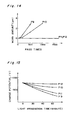
- Fig. 10 shows the variation of charge potential relative to light irradiation time.
- Fig. 11 graphically shows the photosensitivity relative to light irradiation time.
- Fig. 12 graphically shows residual potential relative to light irradiation time.
- Each of these characteristics corresponds to light permeability on the top surfaces of photosensitive layers. It is understood from these results that those multiple optical layers showing less values of light permeability throughout extensive wavelength regions respectively give less deterioration in characteristics.
- All the photosensitive layers have a surface resistance value in excess of 10 13 to 10 14 ⁇ .
- the samples P5 through P8 respectively have multiple optical layers each having 10 10 through 10 14 ⁇ of resistance value on the top surface, and then the attenuation characteristics of charge potential thereof in the dark are detected.
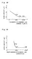
- Fig. 13 graphically shows the relation between the surface resistance of multiple optical layers and attenuation factors in the dark. It is noted that the attenuation in the dark is large when the surface resistance value ranges from 10 10 to 10 11 ⁇ .
- the surface resistance value shall be a minimum of 10 11 ⁇ , preferably in excess of 10130.
- the invention is not solely applicable to the organic photosensitive layer, but the invention generates identical effect even when using inorganic photosensitive layer made from Se or a-Si for example.
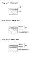
- Fig. 5 shows a sectional view of a electrophotographic photosensitive body.
- an aluminum-made substrates 12 are coated with an organic photosensitive layer 11 having a thickness of about 20 ⁇ m.
- the organic photosensitive layer 11 includes a charge generating layer 11 a and a charge transfer layer 11 b being formed on the substrate 12 in this order.
- a multiple optical film 10 composed of Ti0 2 layers and Si0 2 layers is formed on the charge transfer layer 11 b, and then a diamond-like carbon film 13 is formed on the surface of the multiple optical film 10 by applying the screen-mesh plasma-injected CVD process.
- samples P9 through P12 were prepared.
- the sample P9 only an organic photosensitive layer is formed on an electrically conductive substrate.
- a multiple optical film which is composed of Ti0 2 layers and Si0 2 layers, is formed on the photosensitive layer.
- a diamond-like carbon film is formed on the organic photosensitive layer.
- a multiple optical film which is composed of Ti0 2 layers and Si0 2 layers, is formed on the photosensitive layer, and further a diamond-like carbon film is formed on the multiple optical film.
- each of the multiple optical films is composed of the combination of 20 strums of first layers each of which is composed of a Ti0 2 layer having thickness of 700A and a Si0 2 layer having thickness of 1000A, and 20 strums of second layers each of which is composed of a Ti0 2 layer having thickness of 500A and a Si0 2 layer having thickness of 700A.
- the diamond-like carbon films of the samples P11, 12 respectively have thickness of 200A and Noop hardness of 1200kg/mm 2. Every sample P9-P10 has a surface resistance of 10 13 -10 14 ⁇ .
- a sliding test was executed in comparison with each other. While feeding toners to the surface of each sample, and pressing each blade against the surface of each sample with load of 100g, the sample was repeatedly slided to the blade.
- Fig. 14 graphically shows the relation between the number of sliding movements performed in the test and the worn amount on surface of the tested samples.
- the samples P9, P10 devoid of the diamond-like carbon film on the surface were superficially abraded after completing several scores up to 100 times of abrading tests. On the other hand, no wear was detected on the surface of the diamond-like carbon film even after completing 1,000 times of the abrading test.
- Fig. 15 shows charge potential relative to light irradiation time.
- Fig. 16 shows the photosensitivity relative to light irradiation time.
- Fig. 17 shows relation between residual potential and light irradiation time. As shown in Figs. 15, 16, and 17, top surface layers of the samples P9, P10 devoid of the diamond-like carbon film incurred abrasion, and thus, those characteristics including charge potential, photosensitivity, and residual potential, were noticeable deteriorated.
- Sample P9 having only a photosensitive layer was further remarkably deteriorated.
- the sample P10 superficially coated with the multiple optical film was also worn out, thus resulting in the lowered resistance against degradation of photosensitivity.
- the samples P11, P12 which were superficially coated with the diamond-like carbon film incurred no wear at all, and thus, those characteristics cited above remained unaffected after execution of the abrasion tests.
- the sample P12 which was superficially coated with the diamond-like carbon film in conjunction with the multiple optical film remained free from deterioration of photosensitivity after completing the abrasion tests.
- three samples P13, P14 and P15 were prepared.
- a multiple optical film composed of Ti0 2 layers and Si0 2 layers was formed on the organic photosensitive layer, and then is coated with a diamond-like carbon film having Noop hardness of 1,000kg/mm 2.
- the diamond-like carbon film of the sample P13 has thickness of 1000A.
- the diamond-like carbon film of the sample P14 has 1500A.
- the diamond-like carbon film of the sample P15 has thickness of 2000A.
- Fig. 18 shows the relation between the thickness of diamond-like carbon film and the amount of wear on their surfaces. Based on these test results, it is clear that the thickness of at least 1,500A should be provided for the diamond-like carbon film, desirably more than the thickness of 2,000 ⁇ should be provided in order that the underlaid photosensitive layers can fully be protected without incurring wear at all.
- three samples P16, P17, and P18 were prepared.
- a multiple optical film composed of Ti0 2 layers and Si0 2 layers is formed on the organic photosensitive layer, and a diamond-like carbon film which has the thickness of 2000A is formed on the multiple optical film.
- the diamond-like carbon film of the sample P16 has Noop hardness of 800kg/mm 2.
- the diamond-like carbon film of the sample P17 has Noop hardness of 1,000kg/m M 2.
- the diamond-like carbon film of the sample P18 has Noop hardness of 2,000kg/mm 2 .
- Fig. 19 shows the relation between Noop hardness of diamond-like carbon films and the amount of wear on their surfaces. Based on these test results, it is clear that the Noop hardness of at least 1 ,000kg/mm2 should be provided for the diamond-like carbon film.
- Samples P19 through 22 were prepared, which respectively have diamond-like carbon films of resistance of 10 10 -10 14 ⁇ .
- samples P9 through P22 were prepared. These samples P9 through P22 respectively have the above mentioned compositions formed on cylindrical aluminum substrates and different surface resistance values, and then, the image conditions in those samples P9 through P12 are evaluated by actually running a printer.
- Tables 7 and 8 indicates the result of test.
- the multiple optical films are formed by applying an evaporation process, and yet, the diamond-like carbon film is formed by applying the screen-mesh plasma-injected CVD process.
- the multiple optical film and the diamond-like carbon film can also by synthesized by applying any proper means other than those processes described above.
- the invention can provide an extremely durable photosensitive body by effectively forming a diamond-like carbon film having ideally physical characteristics on the top surface of a photosensitive layer, and as a result, the invention offers extremely useful industrial advantage.
- the invention does not specify the kind, material and shape of the electrophotographic photosensitive layers, but the invention can widely provide useful effect for any object.
- the invention when applying the invention to the electrophotographic photosensitive layer using organic photosensitive material, it extremely improves the resistance against wear, resistance against ozone, and the resistance against light.
- the invention realizes pollution-free, inexpensive, and extremely durable photosensitive drums, thus significantly contributing to the progress of a variety of electrophotographic apparatuses including copying apparatuses.
Landscapes
- Physics & Mathematics (AREA)
- General Physics & Mathematics (AREA)
- Chemical & Material Sciences (AREA)
- Inorganic Chemistry (AREA)
- Photoreceptors In Electrophotography (AREA)
Applications Claiming Priority (4)
| Application Number | Priority Date | Filing Date | Title |
|---|---|---|---|
| JP2176709A JPH0466954A (ja) | 1990-07-04 | 1990-07-04 | 電子写真用感光体 |
| JP176709/90 | 1990-07-04 | ||
| JP247714/90 | 1990-09-17 | ||
| JP2247714A JPH04125566A (ja) | 1990-09-17 | 1990-09-17 | 電子写真感光体 |
Publications (1)
| Publication Number | Publication Date |
|---|---|
| EP0465984A1 true EP0465984A1 (de) | 1992-01-15 |
Family
ID=26497514
Family Applications (1)
| Application Number | Title | Priority Date | Filing Date |
|---|---|---|---|
| EP91110902A Withdrawn EP0465984A1 (de) | 1990-07-04 | 1991-07-02 | Lichtempfindlicher Körper verwendet in Elektrophotographie |
Country Status (2)
| Country | Link |
|---|---|
| US (1) | US5168023A (de) |
| EP (1) | EP0465984A1 (de) |
Cited By (1)
| Publication number | Priority date | Publication date | Assignee | Title |
|---|---|---|---|---|
| EP0810099A3 (de) * | 1996-05-28 | 1998-07-22 | Eastman Kodak Company | Ein Laser absorbierende Bildaufzeichnungstrommel für Abtaster |
Families Citing this family (12)
| Publication number | Priority date | Publication date | Assignee | Title |
|---|---|---|---|---|
| DE59309954D1 (de) * | 1992-12-21 | 2000-03-16 | Balzers Hochvakuum | Optisches Bauelement, Verfahren zur Herstellung einer Schicht, Schicht bzw. Schichtsystem und Verwendung des Bauelementes |
| JPH07295409A (ja) * | 1994-04-25 | 1995-11-10 | Canon Inc | 加熱定着装置及びその製造方法 |
| US5840455A (en) * | 1995-05-24 | 1998-11-24 | Ricoh Company, Ltd. | Electrophotographic photoconductor |
| US5674621A (en) * | 1996-01-29 | 1997-10-07 | Eastman Kodak Company | Fuser members with an outermost layer of a fluorinated diamond like carbon |
| US5900342A (en) * | 1996-04-26 | 1999-05-04 | Eastman Kodak Company | Photoconductive element having an outermost layer of a fluorinated diamond-like carbon and method of making the same |
| US5728496A (en) * | 1996-05-24 | 1998-03-17 | Eastman Kodak Company | Electrostatographic apparatus and method for improved transfer of small particles |
| US5849445A (en) * | 1998-02-13 | 1998-12-15 | Eastman Kodak Company | Multilayer photoconductive elements having low dark decay |
| US5849443A (en) * | 1998-02-13 | 1998-12-15 | Eastman Kodak Company | Method of making multilayer electrophotographic elements |
| US6366751B1 (en) * | 1999-09-17 | 2002-04-02 | Ricoh Company, Ltd. | Image forming apparatus including preselected range between charge injection layer and voltage potential |
| US9166116B2 (en) | 2012-05-29 | 2015-10-20 | Formosa Epitaxy Incorporation | Light emitting device |
| CN106252491A (zh) | 2012-05-29 | 2016-12-21 | 晶元光电股份有限公司 | 发光装置 |
| JP6015160B2 (ja) * | 2012-06-22 | 2016-10-26 | 富士ゼロックス株式会社 | 電子写真感光体、プロセスカートリッジ、及び画像形成装置 |
Family Cites Families (19)
| Publication number | Priority date | Publication date | Assignee | Title |
|---|---|---|---|---|
| IT1116037B (it) * | 1979-04-23 | 1986-02-10 | Sigma Tau Ind Farmaceuti | Esteri e ammidi di acil carnitine loro procedimenti di preparazione e loro uso terapeutico |
| US4403026A (en) * | 1980-10-14 | 1983-09-06 | Canon Kabushiki Kaisha | Photoconductive member having an electrically insulating oxide layer |
| JPS5767932A (en) * | 1980-10-16 | 1982-04-24 | Olympus Optical Co Ltd | Electrophotographic receptor |
| JPS57114146A (en) * | 1981-01-08 | 1982-07-15 | Nippon Telegr & Teleph Corp <Ntt> | Electrophotographic receptor |
| JPS59104667A (ja) * | 1982-12-08 | 1984-06-16 | Canon Inc | 転写制御方法 |
| JPS6061761A (ja) * | 1983-09-16 | 1985-04-09 | Sumitomo Electric Ind Ltd | 電子写真用感光体 |
| JPS61255352A (ja) * | 1985-05-08 | 1986-11-13 | Minolta Camera Co Ltd | 感光体 |
| JPS61264355A (ja) * | 1985-05-20 | 1986-11-22 | Matsushita Electric Ind Co Ltd | 電子写真用感光体 |
| JPS61266567A (ja) * | 1985-05-22 | 1986-11-26 | Minolta Camera Co Ltd | 保護膜成造方法 |
| JPS6253786A (ja) * | 1985-09-03 | 1987-03-09 | Asahi Chem Ind Co Ltd | 純水または超純水の製造方法 |
| JPS62192753A (ja) * | 1986-02-19 | 1987-08-24 | Sharp Corp | 電子写真感光体 |
| JPS62226158A (ja) * | 1986-03-27 | 1987-10-05 | Sharp Corp | 電子写真感光体 |
| JPS62226558A (ja) * | 1986-03-27 | 1987-10-05 | Toshiba Battery Co Ltd | 扁平形電池 |
| JPS6325662A (ja) * | 1986-07-18 | 1988-02-03 | Fuji Electric Co Ltd | 電子写真感光体 |
| JPS63118754A (ja) * | 1986-11-07 | 1988-05-23 | Seiko Epson Corp | 電子写真感光体 |
| US4837137A (en) * | 1986-12-05 | 1989-06-06 | Fuji Electric Co., Ltd. | Electrophotographic photoreceptor |
| US4939056A (en) * | 1987-09-25 | 1990-07-03 | Minolta Camera Kabushiki Kaisha | Photosensitive member |
| JPH0214870A (ja) * | 1988-06-30 | 1990-01-18 | Sumitomo Metal Mining Co Ltd | 酸化物超電導体の製造方法 |
| US5046001A (en) * | 1988-06-30 | 1991-09-03 | Ibm Corporation | Method for accessing selected windows in a multi-tasking system |
-
1991
- 1991-07-02 US US07/724,887 patent/US5168023A/en not_active Expired - Lifetime
- 1991-07-02 EP EP91110902A patent/EP0465984A1/de not_active Withdrawn
Non-Patent Citations (5)
| Title |
|---|
| DATABASE WPIL , no.82-71012E Derwent Publications Ltd,London,GB, & JP-a-57114146 (Nippon Telegr. & Teleph.) * |
| DATABASE WPIL,no. 87-003976 Derwent Publications Ltd, London,GB, & JP-A-61264355 (MATSUSHITA ELEC. IND. K.K.) * |
| DATABASE WPIL,no.87-087739 Derwent Publications Ltd,London,GB, & JP-A-62053786(Minolta Camera K.K.) * |
| PATENT ABSTRACTS OF JAPAN vol. 11, no. 107 (P-563)(2554) 4 April 1987 & JP-A-61 255 352 ( MINOLTA CAMERA CO. LTD. ) 13 November 1986 * |
| PATENT ABSTRACTS OF JAPAN vol. 12, no. 233 (P-724)(3080) 5 July 1988 & JP-A-63 025 662 ( FUJI ELECTRIC CO. LTD. ) 3 February 1988 * |
Cited By (1)
| Publication number | Priority date | Publication date | Assignee | Title |
|---|---|---|---|---|
| EP0810099A3 (de) * | 1996-05-28 | 1998-07-22 | Eastman Kodak Company | Ein Laser absorbierende Bildaufzeichnungstrommel für Abtaster |
Also Published As
| Publication number | Publication date |
|---|---|
| US5168023A (en) | 1992-12-01 |
Similar Documents
| Publication | Publication Date | Title |
|---|---|---|
| US5168023A (en) | Photosensitive element used in electrophotography | |
| EP2093618B1 (de) | Bilderzeugungsvorrichtung und Prozesskartusche | |
| US4869982A (en) | Electrophotographic photoreceptor containing a toner release material | |
| EP0594453A2 (de) | Verfahren zur Abscheidung eines Films für ein lichtempfindliches Element, des lichtempfindliche Element, Vorrichtung zum Herstellen abgeschiedener Filme, Verfahren zur Reinigung dieser Vorrichtung | |
| KR101548788B1 (ko) | 전자사진 감광 부재, 프로세스 카트리지, 및 전자사진 장치 | |
| JP2829629B2 (ja) | アモルファスシリコン系感光体を用いた電子写真法による画像形成方法及び電子写真装置 | |
| US7157197B2 (en) | Electrophotographic photosensitive member | |
| CN101196696A (zh) | 电子照相感光体和包括其的图像形成装置 | |
| US5422209A (en) | Electrophotographic photoreceptor having a photoconductive layer of amorphous silicon and surface layer | |
| JP2008191488A (ja) | 電子写真装置 | |
| US5352555A (en) | Electrophotographic photoreceptor and electrophotographic process therefor | |
| US5268247A (en) | Electrophotographic copying machine and electrophotographic member therefor and method of forming an electrophotographic member | |
| US10545417B1 (en) | Electrophotographic photoconductor, image forming apparatus, and image forming method | |
| US5087543A (en) | Electrophotographic printer | |
| US4837099A (en) | Multilayer photoconductor for electrophotography | |
| JP4136622B2 (ja) | 画像形成装置及びプロセスカートリッジ | |
| JPH10246997A (ja) | 電子写真装置 | |
| US5876886A (en) | Light-receiving member and electrophotographic apparatus making use of the same | |
| US5462827A (en) | Electrophotographic photoreceptor and electrophotographic process | |
| JP5412883B2 (ja) | 電子写真感光体、それを用いた画像形成方法、画像形成装置及び画像形成装置用プロセスカートリッジ | |
| JP2775477B2 (ja) | 電子写真用感光体 | |
| JPH1165153A (ja) | 電子写真感光体及び画像形成装置 | |
| JP2008176055A (ja) | 電子写真感光体及びこれを用いた画像形成装置 | |
| JP3661459B2 (ja) | 電子写真感光体及び画像形成装置とプロセスカートリッジ | |
| JP2006189823A (ja) | 電子写真感光体 |
Legal Events
| Date | Code | Title | Description |
|---|---|---|---|
| PUAI | Public reference made under article 153(3) epc to a published international application that has entered the european phase |
Free format text: ORIGINAL CODE: 0009012 |
|
| 17P | Request for examination filed |
Effective date: 19910702 |
|
| AK | Designated contracting states |
Kind code of ref document: A1 Designated state(s): DE FR GB |
|
| 17Q | First examination report despatched |
Effective date: 19941004 |
|
| STAA | Information on the status of an ep patent application or granted ep patent |
Free format text: STATUS: THE APPLICATION HAS BEEN WITHDRAWN |
|
| 18W | Application withdrawn |
Withdrawal date: 19950331 |