EP0480475B1 - Kodeeinstellungsschaltung - Google Patents
Kodeeinstellungsschaltung Download PDFInfo
- Publication number
- EP0480475B1 EP0480475B1 EP91117462A EP91117462A EP0480475B1 EP 0480475 B1 EP0480475 B1 EP 0480475B1 EP 91117462 A EP91117462 A EP 91117462A EP 91117462 A EP91117462 A EP 91117462A EP 0480475 B1 EP0480475 B1 EP 0480475B1
- Authority
- EP
- European Patent Office
- Prior art keywords
- field effect
- effect transistor
- code setting
- thin film
- setting circuit
- Prior art date
- Legal status (The legal status is an assumption and is not a legal conclusion. Google has not performed a legal analysis and makes no representation as to the accuracy of the status listed.)
- Expired - Lifetime
Links
- 239000010409 thin film Substances 0.000 claims description 38
- 230000005669 field effect Effects 0.000 claims 12
- 230000003071 parasitic effect Effects 0.000 description 9
- 230000000630 rising effect Effects 0.000 description 7
- 238000010586 diagram Methods 0.000 description 5
- 230000007257 malfunction Effects 0.000 description 3
- 238000009966 trimming Methods 0.000 description 3
- 230000009471 action Effects 0.000 description 2
- 230000003111 delayed effect Effects 0.000 description 2
- 238000004519 manufacturing process Methods 0.000 description 2
- 239000000758 substrate Substances 0.000 description 2
- 230000008859 change Effects 0.000 description 1
- 230000007547 defect Effects 0.000 description 1
- 238000000034 method Methods 0.000 description 1
- 230000004048 modification Effects 0.000 description 1
- 238000012986 modification Methods 0.000 description 1
- 230000008569 process Effects 0.000 description 1
- 230000004044 response Effects 0.000 description 1
Images


Classifications
-
- G—PHYSICS
- G11—INFORMATION STORAGE
- G11C—STATIC STORES
- G11C17/00—Read-only memories programmable only once; Semi-permanent stores, e.g. manually-replaceable information cards
- G11C17/14—Read-only memories programmable only once; Semi-permanent stores, e.g. manually-replaceable information cards in which contents are determined by selectively establishing, breaking or modifying connecting links by permanently altering the state of coupling elements, e.g. PROM
- G11C17/18—Auxiliary circuits, e.g. for writing into memory
-
- G—PHYSICS
- G05—CONTROLLING; REGULATING
- G05F—SYSTEMS FOR REGULATING ELECTRIC OR MAGNETIC VARIABLES
- G05F1/00—Automatic systems in which deviations of an electric quantity from one or more predetermined values are detected at the output of the system and fed back to a device within the system to restore the detected quantity to its predetermined value or values, i.e. retroactive systems
- G05F1/10—Regulating voltage or current
- G05F1/46—Regulating voltage or current wherein the variable actually regulated by the final control device is DC
- G05F1/468—Regulating voltage or current wherein the variable actually regulated by the final control device is DC characterised by reference voltage circuitry, e.g. soft start, remote shutdown
-
- G—PHYSICS
- G05—CONTROLLING; REGULATING
- G05F—SYSTEMS FOR REGULATING ELECTRIC OR MAGNETIC VARIABLES
- G05F3/00—Non-retroactive systems for regulating electric variables by using an uncontrolled element, or an uncontrolled combination of elements, such element or such combination having self-regulating properties
- G05F3/02—Regulating voltage or current
- G05F3/08—Regulating voltage or current wherein the variable is DC
- G05F3/10—Regulating voltage or current wherein the variable is DC using uncontrolled devices with non-linear characteristics
- G05F3/16—Regulating voltage or current wherein the variable is DC using uncontrolled devices with non-linear characteristics being semiconductor devices
- G05F3/20—Regulating voltage or current wherein the variable is DC using uncontrolled devices with non-linear characteristics being semiconductor devices using diode- transistor combinations
- G05F3/24—Regulating voltage or current wherein the variable is DC using uncontrolled devices with non-linear characteristics being semiconductor devices using diode- transistor combinations wherein the transistors are of the field-effect type only
-
- G—PHYSICS
- G01—MEASURING; TESTING
- G01R—MEASURING ELECTRIC VARIABLES; MEASURING MAGNETIC VARIABLES
- G01R31/00—Arrangements for testing electric properties; Arrangements for locating electric faults; Arrangements for electrical testing characterised by what is being tested not provided for elsewhere
- G01R31/28—Testing of electronic circuits, e.g. by signal tracer
- G01R31/317—Testing of digital circuits
- G01R31/31702—Testing digital circuits including elements other than semiconductor transistors, e.g. biochips, nanofabrics, mems, chips with magnetic elements
Definitions
- the present invention relates to a code setting circuit according to the preamble part of claim 1.
- Such a code setting circuit is known from JP-A-12 78 746.
- an additional circuit which can adjust the reference voltage or the circuit current within a tolerance range of the required standard by a trimming performed in the process of manufacturing the integrated circuit.
- This trimming has a property of permanently maintaining the adjusted value unchangeably, so that the reference voltage or the circuit current is fixed if the trimming is conducted one time in the manufacturing process, and therefore, re-adjustment is no longer possible in actual application of the integrated circuit. Therefore, the additional circuit is required to be highly reliable so as to operate without error.
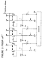
- the shown circuit includes a constant current circuit composed of a MOS transistor M19 and a constant current source Io connected in series between a high voltage V DD and the ground so as to allow a constant current I M10 to flow through the MOS transistor M19.
- the shown circuit also includes three transistors M20, M21 and M22 connected to flow the constant current I M10 determined by the constant current circuit, and three thin film resistors R7, R8 and R9 connected in series to the transistors M20, M21 and M22, respectively.
- Each of the transistors M20, M21 and M22 and a corresponding one of the resistors R7, R8 and R9 form a ratio circuit.
- a resistance of the resistors R7, R8 and R9 is set to be sufficiently lower than an ON resistance of the transistors M20, M21 and M22. Therefore, in the shown condition, all of three nodes A, B and C are at a low level, and three inverters I 13 to I 15 having an input connected to the nodes A, B and C, respectively, output a high level signal to a decoder 300, respectively.
- the thin film resistors R7, R8 and R9 are selectively fused or broken off by applying a high voltage to only a selected one (or ones) of pads 30, 32 and 34 associated to the thin film resistors R7, R8 and R9, respectively, so that a large current is caused to flow through a selected thin film resistor and an intense heat is generated in the selected thin film resistor
- the broken thin film resistor R8 ideally have an infinite resistance, and therefore, the node B is brought into a high level by action of the transistor M21.
- the inverter I 14 outputs a low level signal to the decoder 300.
- a desired binary code of three bits can be supplied to the decoder 300.
- the thin film resistors R10 to R12 are set to be on the order of 100 ⁇ . Therefore, if the transistors M24, M26 and M28 are set to have an ON resistance of not less than 1 K ⁇ , nodes D, E and F become a low level when the thin film resistors R10 to R12 are not broken off. In this case, accordingly, associated inverters I 16 to I 18 output a high level signal to a decoder 300.
- the transistors M24, M26 and M28 are turned on only for the short period of time just after the power-on, but since P-channel MOS transistors M23, M25 and M27 having a gate controlled by an inverted signal of the nodes D, E and F are provided in parallel to the transistors M24, M26 and M28, respectively, respective once-determined levels of the nodes nodes D, E and F are stably maintained.
- the circuit shown in Figure 2 can realize a greatly stable code setting circuit.
- the circuit shown in Figure 2 is disadvantageous in the following point:
- each of pads 40,42 and 44 connected to the thin film resistors is connected through the two parallel-connected P-channel transistors to the high voltage V DD .
- Each of the P-channel transistors is formed in an n-well of a substrate, as shown in Figure 3.
- the substrate generally designated by Reference Numeral 10 is of a p-type, and has the n-well 12, in which an n + region 14 is formed for biasing the n-well 12.
- a p + drain region 16 and a p + source region 18 of the P-channel transistor are formed in the n-well 12, and a gate 20 is located above a channel region between the p + drain region 16 and the p + source region 18.
- the drain region 16 is connected directly to a pad 22 connected to the thin film resistor, and the source region 18 and the n + region 14 are connected to a high voltage supply line V DD , which has a parasitic capacitance C.
- a high voltage is applied to a desired pad so as to break off the associated thin film resistor, while maintaining the high voltage supply line V DD in a floating condition.
- the pad since the pad is connected to the drain of the P-channel transistor, the pad is connected to the high voltage supply line V DD through a PN junction diode which is formed between the drain region 16 and the n-well 12 and which is biased in a forward direction by the high voltage applied to the pad.
- the circuit shown in Figure 2 has encountered a problem in which the thin film resistor cannot be sufficiently fused or broken off since a rising speed of a fusing-off pulse is lowered due to the parasitic capacitance of the voltage supply line V DD .
- Another object of the present invention is to provide a code setting circuit capable of increasing a rising speed of a fusing-off pulse applied to a pad connected to a thin film resistor so that a broken-off condition of the thin film resistor can be improved, and also capable of suppressing an increase of a leakage current with the passage of time, whereby reliability of the code setting circuit can be remarkably improved.
- the second transistor functions to isolate the fusing-off pulse application pad from a PN junction diode which is formed within the first transistor and which is biased in a forward direction. Therefore, when a high voltage pulse is applied to the fusing-off pulse application pad so as to break off the associated thin film resistor, an electric current does not flow through the PN junction diode formed within the first transistor, into the first voltage supply line having a parasitic capacitance, since the electric current is blocked by the second transistor. Accordingly, the fusing-off pulse having an abrupt rising edge is applied to the thin film resistor, and therefore, the thin film resistor can be completely broken or cut off.
- FIG. 4 there is shown a circuit diagram of a first embodiment of the code setting circuit in accordance with the present invention.
- the shown code setting circuit includes three unitary circuits 50, 52 and 54 each generating one bit of the code setting signal to a code generation circuit composed of a decoder 101.
- Each of the unitary circuits 50, 52 and 54 includes a P-channel enhancement transistor M2, M4 or M6 having a source connected to a high voltage supply line V DD and a gate connected to commonly receive a power-on signal Sp.
- Another P-channel enhancement transistor M1, M3 or M5 is connected in parallel to the P-channel enhancement transistor M2, M4 or M6, in such a manner that a source and a drain of the P-channel enhancement transistor M1, M3 or M5 is connected to the source and a drain of the P-channel enhancement transistor M2, M4 or M6, respectively.
- a gate of the P-channel enhancement transistor M1, M3 or M5 is connected to an output of an inverter I 1 , I 3 or I 5 having an input connected to the drain of the P-channel enhancement transistor M2, M4 or M6.
- an N-channel depletion transistors M7, M8 or M9 is connected at its drain and its gate to the drain of the P-channel enhancement transistor M2, M4 or M6.
- a source of the N-channel depletion transistors M7, M8 or M9 is connected to an associated thin film resistor R1, R2 or R3 and also to an associated pad 110, 111 or 112.
- the drain of the P-channel enhancement transistor M2, M4 or M6 is connected to an input of another inverter I 2 , I 4 or I 6 , which has an output supplying a binary signal to the input of the decoder 101.
- the pads 110 to 112 are connected through a resistance of a few kilo-ohms to the parasitic capacitance of the high voltage supply line V DD , since influence of the parasitic capacitance is negligible, the rising speed of the fusing-off pulse is not delayed.
- FIG 5 there is shown a second embodiment of the code setting circuit in accordance with the present invention.
- the same elements as those shown in Figure 4 are given the same Reference Numerals, and explanation thereof will be omitted.
- the second embodiment is characterized by comprising three N-channel enhancement transistors M16, M17 and M18, in place of the three N-channel depletion transistors M7, M8 and M9, respectively.
- a gate of each of the N-channel enhancement transistors M16, M17 and M18 is connected to the high voltage supply line V DD .
- the N-channel enhancement transistors M16, M17 or M18 connected to the selected pad 110, 111 or 112 is maintained in an OFF condition. Therefore, since the selected pad 110, 111 or 112 are isolated from the parasitic capacitance of the high voltage supply line V DD , the fusing-off pulse is subjected to no influence of the parasitic capacitance, and therefore, the fusing-off pulse having a sharp rising edge is applied to the selected thin film resistor.
Landscapes
- Engineering & Computer Science (AREA)
- Physics & Mathematics (AREA)
- Microelectronics & Electronic Packaging (AREA)
- General Physics & Mathematics (AREA)
- Radar, Positioning & Navigation (AREA)
- Automation & Control Theory (AREA)
- Electromagnetism (AREA)
- Nonlinear Science (AREA)
- Semiconductor Integrated Circuits (AREA)
- Testing Or Measuring Of Semiconductors Or The Like (AREA)
- Metal-Oxide And Bipolar Metal-Oxide Semiconductor Integrated Circuits (AREA)
- Design And Manufacture Of Integrated Circuits (AREA)
- Compression, Expansion, Code Conversion, And Decoders (AREA)
Claims (4)
- Code-Einstellungsschaltung zur Einstellung einer Eingabe einer Code-Erzeugungsschaltung, wobei die Code-Einstellungsschaltung enthält:einen ersten Feldeffekttransistor (M2) eines ersten Leitfähigkeitstyps mit einem Hauptstromweg, der mit einem Ende mit einer Spannungsversorgungsleitung (VDD) verbunden ist und bei dem ein Gateanschluß zum gemeinsamen Empfang eines Leistung-AN-Signals SP geschaltet ist;einen zweiten Feldeffekttransistor (M1) mit einem Hauptstromweg, der parallel zum Hauptstromweg des ersten Feldeffekttransistors (M2) geschaltet ist, und bei dem ein Gateanschluß mit einer Ausgabe eines ersten Inverters (I1) verbunden ist, der einen mit dem zweiten Ende des Hauptstromweges des ersten Feldeffekttransistors (M2) verbundenen Eingang hat;einen Dünnfilmwiderstand (R1), der mit einem Ende mit einem Durchbrenn-Pulsanlegungsanschluß verbunden ist, und mit dem zweiten Ende mit einer zweiten Spannungsversorgungsleitung (GND) verbunden ist; undeinen zweiten Inverter (I2) mit einem Eingang, der mit dem zweiten Ende des Hauptstromweges des ersten Feldeffekttransistors (M2) verbunden ist, und einen Ausgang hat, der ein binäres Signal an den Eingang der Code-Erzeugungsschaltung liefert;dadurch gekennzeichnet, daß die Code-Einstellungsschaltung außerdem umfaßt:einen dritten Feldeffekttransistor (M7) eines zweiten Leitfähigkeitstyps - entgegengesetzt dem ersten Leitfähigkeitstyp -, wobei der dritte Feldeffekttransistor einen Hauptstromweg hat, dessen erstes Ende mit dem zweiten Ende des Hauptstromweges des ersten Feldeffekttransistors (M2) und dessen zweites Ende mit dem Durchbrenn-Pulsanlegungsanschluß und dem ersten Ende des Dunnfilmwiderstands (R1) verbunden ist.
- Code-Einstellungsschaltung nach Anspruch 1, bei der die erste Spannungsversorgungsleitung (VDD) eine Hochspannungszufuhrleitung und die zweite Spannungsversorgungsleitung eine Masseleitung ist, und wobei der erste und zweite Feldeffekttransistor (M2, M1) vom P-Kanal-Typ und der dritte Feldeffekttransistor (M7) vom N-Kanaltyp sind.
- Code-Einstellungsschaltung nach einem der Ansprüche 1 oder 2,
bei der der dritte Feldeffekttransistor (M7) vom Verarmungstyp ist und einen Gateanschluß hat, der mit dem zweiten Ende des Hauptstromweges des ersten Feldeffekttransistors (M2) verbunden ist. - Code-Einstellungsschaltung nach einem der Ansprüche 1 oder 2,
bei der der dritte Feldeffekttransistor (M7) vom Anreicherungstyp ist und einen Gateanschluß hat, der mit der Hochspannungszufuhrleitung (VDD) verbunden ist.
Applications Claiming Priority (2)
| Application Number | Priority Date | Filing Date | Title |
|---|---|---|---|
| JP274790/90 | 1990-10-12 | ||
| JP2274790A JP2679390B2 (ja) | 1990-10-12 | 1990-10-12 | コード設定回路 |
Publications (2)
| Publication Number | Publication Date |
|---|---|
| EP0480475A1 EP0480475A1 (de) | 1992-04-15 |
| EP0480475B1 true EP0480475B1 (de) | 1996-08-28 |
Family
ID=17546600
Family Applications (1)
| Application Number | Title | Priority Date | Filing Date |
|---|---|---|---|
| EP91117462A Expired - Lifetime EP0480475B1 (de) | 1990-10-12 | 1991-10-14 | Kodeeinstellungsschaltung |
Country Status (4)
| Country | Link |
|---|---|
| US (1) | US5173616A (de) |
| EP (1) | EP0480475B1 (de) |
| JP (1) | JP2679390B2 (de) |
| DE (1) | DE69121661T2 (de) |
Families Citing this family (15)
| Publication number | Priority date | Publication date | Assignee | Title |
|---|---|---|---|---|
| US5418487A (en) * | 1992-09-04 | 1995-05-23 | Benchmarg Microelectronics, Inc. | Fuse state sense circuit |
| JP2991575B2 (ja) * | 1992-10-08 | 1999-12-20 | 沖電気工業株式会社 | 半導体集積回路 |
| US5315177A (en) * | 1993-03-12 | 1994-05-24 | Micron Semiconductor, Inc. | One time programmable fully-testable programmable logic device with zero power and anti-fuse cell architecture |
| JP2707954B2 (ja) * | 1993-09-01 | 1998-02-04 | 日本電気株式会社 | コード設定回路 |
| JP2699877B2 (ja) * | 1994-07-26 | 1998-01-19 | 日本電気株式会社 | コード設定回路 |
| US6198337B1 (en) * | 1996-12-11 | 2001-03-06 | A & Cmos Communications Device Inc. | Semiconductor device for outputting a reference voltage, a crystal oscillator device comprising the same, and a method of producing the crystal oscillator device |
| FR2797086B1 (fr) | 1999-07-30 | 2001-10-12 | St Microelectronics Sa | Cellule logique a programmation unique |
| JP4301760B2 (ja) * | 2002-02-26 | 2009-07-22 | 株式会社ルネサステクノロジ | 半導体装置 |
| US9453251B2 (en) | 2002-10-08 | 2016-09-27 | Pfenex Inc. | Expression of mammalian proteins in Pseudomonas fluorescens |
| KR100739240B1 (ko) * | 2003-10-07 | 2007-07-12 | 에스티마이크로일렉트로닉스 엔.브이. | 반도체 소자의 리던던시 입출력 퓨즈 회로 |
| US8603824B2 (en) | 2004-07-26 | 2013-12-10 | Pfenex, Inc. | Process for improved protein expression by strain engineering |
| JP2006059969A (ja) * | 2004-08-19 | 2006-03-02 | Sony Corp | 半導体装置 |
| US9580719B2 (en) | 2007-04-27 | 2017-02-28 | Pfenex, Inc. | Method for rapidly screening microbial hosts to identify certain strains with improved yield and/or quality in the expression of heterologous proteins |
| JP5444553B2 (ja) | 2007-04-27 | 2014-03-19 | フェネックス インコーポレイテッド | 微生物宿主を迅速にスクリーニングして、異種タンパク質発現の収率および/または質が改善されている特定の株を同定する方法 |
| JP6115277B2 (ja) * | 2013-04-16 | 2017-04-19 | 富士電機株式会社 | 半導体装置 |
Family Cites Families (4)
| Publication number | Priority date | Publication date | Assignee | Title |
|---|---|---|---|---|
| US4223277A (en) * | 1978-12-27 | 1980-09-16 | Harris Corporation | Electrically alterable field effect transistor amplifier configuration |
| US4546455A (en) * | 1981-12-17 | 1985-10-08 | Tokyo Shibaura Denki Kabushiki Kaisha | Semiconductor device |
| US4608530A (en) * | 1984-11-09 | 1986-08-26 | Harris Corporation | Programmable current mirror |
| US4716302A (en) * | 1986-12-22 | 1987-12-29 | Motorola, Inc. | Identity circuit for an integrated circuit using a fuse and transistor enabled by a power-on reset signal |
-
1990
- 1990-10-12 JP JP2274790A patent/JP2679390B2/ja not_active Expired - Fee Related
-
1991
- 1991-10-14 DE DE69121661T patent/DE69121661T2/de not_active Expired - Fee Related
- 1991-10-14 EP EP91117462A patent/EP0480475B1/de not_active Expired - Lifetime
- 1991-10-15 US US07/775,462 patent/US5173616A/en not_active Expired - Lifetime
Also Published As
| Publication number | Publication date |
|---|---|
| US5173616A (en) | 1992-12-22 |
| DE69121661T2 (de) | 1997-04-03 |
| JP2679390B2 (ja) | 1997-11-19 |
| EP0480475A1 (de) | 1992-04-15 |
| JPH04150050A (ja) | 1992-05-22 |
| DE69121661D1 (de) | 1996-10-02 |
Similar Documents
| Publication | Publication Date | Title |
|---|---|---|
| EP0480475B1 (de) | Kodeeinstellungsschaltung | |
| US5867013A (en) | Startup circuit for band-gap reference circuit | |
| US6329871B2 (en) | Reference voltage generation circuit using source followers | |
| KR940001251B1 (ko) | 전압 제어회로 | |
| EP0305098B1 (de) | CMOS/ECL Konverter-Ausgangspufferschaltung | |
| US4730129A (en) | Integrated circuit having fuse circuit | |
| JPH06204838A (ja) | 基準電圧発生器及び基準電圧の発生方法 | |
| US4890019A (en) | Bilingual CMOS to ECL output buffer | |
| JPH08272467A (ja) | 基板電位発生回路 | |
| US5973530A (en) | Low power, high voltage-tolerant bus holder circuit in low voltage technology | |
| US6441651B2 (en) | High voltage tolerable input buffer | |
| KR20020077035A (ko) | 어드레스 발생 회로 | |
| GB2032717A (en) | Voltage generator circuits and integrated circuits incorporating such circuits | |
| EP0841751B1 (de) | Verzögerungsschaltung | |
| US4290119A (en) | Memory device protected against undesirable supply voltage level | |
| KR100248172B1 (ko) | 반도체 전위 공급 장치 및 이를 이용한 반도체 기억 장치 | |
| EP0644554B1 (de) | Störungsunempfindliche Codeeinstellungsschaltung | |
| JPH06230840A (ja) | バイアス回路 | |
| JP2699828B2 (ja) | 半導体装置の入出力回路 | |
| GB2051382A (en) | Voltage Detecting Circuit | |
| US4571509A (en) | Output circuit having decreased interference between output terminals | |
| KR100480906B1 (ko) | 반도체 메모리 소자의 리페어 회로 | |
| JP2994114B2 (ja) | プログラム回路 | |
| US7084614B2 (en) | Reference voltage generator | |
| JPH10232723A (ja) | 電圧調整回路 |
Legal Events
| Date | Code | Title | Description |
|---|---|---|---|
| PUAI | Public reference made under article 153(3) epc to a published international application that has entered the european phase |
Free format text: ORIGINAL CODE: 0009012 |
|
| 17P | Request for examination filed |
Effective date: 19911014 |
|
| AK | Designated contracting states |
Kind code of ref document: A1 Designated state(s): DE FR GB |
|
| 17Q | First examination report despatched |
Effective date: 19940426 |
|
| GRAH | Despatch of communication of intention to grant a patent |
Free format text: ORIGINAL CODE: EPIDOS IGRA |
|
| GRAA | (expected) grant |
Free format text: ORIGINAL CODE: 0009210 |
|
| GRAH | Despatch of communication of intention to grant a patent |
Free format text: ORIGINAL CODE: EPIDOS IGRA |
|
| AK | Designated contracting states |
Kind code of ref document: B1 Designated state(s): DE FR GB |
|
| REF | Corresponds to: |
Ref document number: 69121661 Country of ref document: DE Date of ref document: 19961002 |
|
| ET | Fr: translation filed | ||
| PLBE | No opposition filed within time limit |
Free format text: ORIGINAL CODE: 0009261 |
|
| STAA | Information on the status of an ep patent application or granted ep patent |
Free format text: STATUS: NO OPPOSITION FILED WITHIN TIME LIMIT |
|
| 26N | No opposition filed | ||
| REG | Reference to a national code |
Ref country code: GB Ref legal event code: IF02 |
|
| REG | Reference to a national code |
Ref country code: GB Ref legal event code: 732E |
|
| REG | Reference to a national code |
Ref country code: FR Ref legal event code: TP |
|
| PGFP | Annual fee paid to national office [announced via postgrant information from national office to epo] |
Ref country code: DE Payment date: 20081014 Year of fee payment: 18 |
|
| PGFP | Annual fee paid to national office [announced via postgrant information from national office to epo] |
Ref country code: FR Payment date: 20081014 Year of fee payment: 18 |
|
| PGFP | Annual fee paid to national office [announced via postgrant information from national office to epo] |
Ref country code: GB Payment date: 20081008 Year of fee payment: 18 |
|
| REG | Reference to a national code |
Ref country code: FR Ref legal event code: ST Effective date: 20100630 |
|
| PG25 | Lapsed in a contracting state [announced via postgrant information from national office to epo] |
Ref country code: FR Free format text: LAPSE BECAUSE OF NON-PAYMENT OF DUE FEES Effective date: 20091102 Ref country code: DE Free format text: LAPSE BECAUSE OF NON-PAYMENT OF DUE FEES Effective date: 20100501 |
|
| PG25 | Lapsed in a contracting state [announced via postgrant information from national office to epo] |
Ref country code: GB Free format text: LAPSE BECAUSE OF NON-PAYMENT OF DUE FEES Effective date: 20091014 |