EP0489559B1 - LDD Metalloxyd-Halbleiter-Feldeffekttransistor und Verfahren zur Herstellung - Google Patents
LDD Metalloxyd-Halbleiter-Feldeffekttransistor und Verfahren zur Herstellung Download PDFInfo
- Publication number
- EP0489559B1 EP0489559B1 EP91311183A EP91311183A EP0489559B1 EP 0489559 B1 EP0489559 B1 EP 0489559B1 EP 91311183 A EP91311183 A EP 91311183A EP 91311183 A EP91311183 A EP 91311183A EP 0489559 B1 EP0489559 B1 EP 0489559B1
- Authority
- EP
- European Patent Office
- Prior art keywords
- impurity
- gate
- semiconductor substrate
- concentration
- extending
- Prior art date
- Legal status (The legal status is an assumption and is not a legal conclusion. Google has not performed a legal analysis and makes no representation as to the accuracy of the status listed.)
- Expired - Lifetime
Links
- 239000004065 semiconductor Substances 0.000 title claims description 23
- 229910044991 metal oxide Inorganic materials 0.000 title claims description 10
- 230000005669 field effect Effects 0.000 title claims description 8
- 238000004519 manufacturing process Methods 0.000 title claims description 8
- -1 LDD metal-oxide Chemical class 0.000 title description 7
- 239000000758 substrate Substances 0.000 claims description 47
- 238000009792 diffusion process Methods 0.000 claims description 27
- 239000012535 impurity Substances 0.000 claims description 23
- 150000004706 metal oxides Chemical class 0.000 claims description 9
- 238000000034 method Methods 0.000 claims description 6
- 230000001154 acute effect Effects 0.000 claims 1
- 229910052698 phosphorus Inorganic materials 0.000 description 11
- 239000011574 phosphorus Substances 0.000 description 11
- OAICVXFJPJFONN-UHFFFAOYSA-N Phosphorus Chemical compound [P] OAICVXFJPJFONN-UHFFFAOYSA-N 0.000 description 7
- 229910052785 arsenic Inorganic materials 0.000 description 6
- 239000000969 carrier Substances 0.000 description 6
- XUIMIQQOPSSXEZ-UHFFFAOYSA-N Silicon Chemical compound [Si] XUIMIQQOPSSXEZ-UHFFFAOYSA-N 0.000 description 4
- RQNWIZPPADIBDY-UHFFFAOYSA-N arsenic atom Chemical compound [As] RQNWIZPPADIBDY-UHFFFAOYSA-N 0.000 description 4
- 238000005530 etching Methods 0.000 description 4
- 238000010884 ion-beam technique Methods 0.000 description 4
- 229910052710 silicon Inorganic materials 0.000 description 4
- 239000010703 silicon Substances 0.000 description 4
- VYPSYNLAJGMNEJ-UHFFFAOYSA-N Silicium dioxide Chemical compound O=[Si]=O VYPSYNLAJGMNEJ-UHFFFAOYSA-N 0.000 description 3
- 238000007796 conventional method Methods 0.000 description 3
- 230000003071 parasitic effect Effects 0.000 description 3
- 229910052814 silicon oxide Inorganic materials 0.000 description 3
- 238000005516 engineering process Methods 0.000 description 2
- 238000005468 ion implantation Methods 0.000 description 2
- 230000000873 masking effect Effects 0.000 description 2
- 229910021420 polycrystalline silicon Inorganic materials 0.000 description 2
- 229920005591 polysilicon Polymers 0.000 description 2
- 230000008569 process Effects 0.000 description 2
- 230000008859 change Effects 0.000 description 1
- 238000010276 construction Methods 0.000 description 1
- 230000003247 decreasing effect Effects 0.000 description 1
- 230000006866 deterioration Effects 0.000 description 1
- 230000000694 effects Effects 0.000 description 1
- 230000005684 electric field Effects 0.000 description 1
- 238000010438 heat treatment Methods 0.000 description 1
- 238000002513 implantation Methods 0.000 description 1
- 238000009413 insulation Methods 0.000 description 1
- 150000002500 ions Chemical class 0.000 description 1
- 230000001590 oxidative effect Effects 0.000 description 1
- 230000009467 reduction Effects 0.000 description 1
Images


Classifications
-
- H—ELECTRICITY
- H10—SEMICONDUCTOR DEVICES; ELECTRIC SOLID-STATE DEVICES NOT OTHERWISE PROVIDED FOR
- H10D—INORGANIC ELECTRIC SEMICONDUCTOR DEVICES
- H10D30/00—Field-effect transistors [FET]
- H10D30/01—Manufacture or treatment
- H10D30/021—Manufacture or treatment of FETs having insulated gates [IGFET]
- H10D30/0223—Manufacture or treatment of FETs having insulated gates [IGFET] having source and drain regions or source and drain extensions self-aligned to sides of the gate
- H10D30/0227—Manufacture or treatment of FETs having insulated gates [IGFET] having source and drain regions or source and drain extensions self-aligned to sides of the gate having both lightly-doped source and drain extensions and source and drain regions self-aligned to the sides of the gate, e.g. lightly-doped drain [LDD] MOSFET or double-diffused drain [DDD] MOSFET
-
- H—ELECTRICITY
- H10—SEMICONDUCTOR DEVICES; ELECTRIC SOLID-STATE DEVICES NOT OTHERWISE PROVIDED FOR
- H10D—INORGANIC ELECTRIC SEMICONDUCTOR DEVICES
- H10D30/00—Field-effect transistors [FET]
- H10D30/60—Insulated-gate field-effect transistors [IGFET]
Definitions
- the present invention relates to a method of making a metal-oxide semiconductor field-effect transistor structure, and particularly to the drain structure of such a semiconductor device. Also, the present invention relates to a metal-oxide semiconductor field-effect transistor structure made by the method.
- the lightly doped drain structure of a metal-oxide semiconductor field effect transistor comprises a lightly doped section starting from a location under one edge of the gate and extending a relatively short distance apart from said location, and a heavily doped section following said lightly doped section and extending a relatively long distance apart from the gate.
- MOSFET metal-oxide semiconductor field effect transistor
- the presence of such lightly doped section ahead of the heavily doped section will cause the strength of the electric field appearing in the vicinity of the drain of the device to be reduced so as to suppress appearance of hot carriers.
- Such hot carriers are liable to invade the gate through the underlying metal oxide and to remain in the gate, and as a result the performance of the device will change with age.
- Adoption of the lightly doped drain structure in a MOSFET improves substantially the reliability of the device.
- the lightly doped section functions as a parasitic resistor, and disadvantageously it will lower the current driving capability of the device.
- a profiled lightly doped drain structure (abbreviated PLDD) was proposed (See the paper "Profiled Lightly Doped Drain (PLDD) Structure for High Reliable NMOSFETs", Y. Toyoshima et al, Digest of Technical Papers, Symposium on VLSI Technology,pp.118-119, 1985).
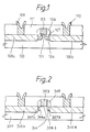
- Fig. 1 shows, in section, a PLDD structure.
- It comprises a P-type silicon substrate 100, a gate insulating layer 101 formed on the top surface of the substrate 100, a gate 103 built on the gate insulating layer 101, an N-type source diffusion layer 108a, and an N-type drain diffusion layer 108b.
- the gate 103 has a surrounding wall 106, and the source and drain diffusion layers 108a and 108b have electrodes 109 and 110 respectively. These electrodes 109 and 110 are embedded in an overlying insulating layer 111.
- the drain diffusion layer is composed of an upper short projection 107 of least concentration of impurity such as arsenic, a surrounding section 104 of less concentration of impurity such as phosphorus, and an elongated section 108b of relatively high concentration of impurity such as arsenic, lying contiguous to the upper projection 107 and surrounding section 104, which end at a location under one edge of the gate 103.
- European patent application EP 0187016 describes a device of this type, at figure 4, and also describes at figures 6 to 9 a second type of MOSFET in which three regions of the LDD structure having less, least (intermediate) and highest impurity concentrations are arranged in series.
- FIG. 2 This type of structure is described at figure 2 herein, where the known MOSFET is shown as comprising: a P-type silicon substrate 300; a gate insulating layer 301 of silicon formed on the top surface of the substrate 300; a gate 303 built on the gate insulation 301; an N-type source diffusion layer 304a and an N-type drain diffusion layer 304b extending toward and ending at first locations under one and the other edges of the gate 303 respectively in opposite directions in the substrate 300; and an N-type source diffusion layer 307a and an N-type drain diffusion layer 307b extending toward and ending at second locations under one and the other edges of the gate 303 respectively in opposite directions in the substrate 300.
- the source diffusion layer is composed of a first relatively short section 304a of least concentration of impurity, a second relatively short section 307a of less concentration of impurity, and a third relatively long section 310a of relatively high concentration of impurity lying contiguous to each other and extending far from the first location in the order named.
- the drain diffusion layer has also the same structure 304b, 307b, 310b.
- the first short sections 304a and 304b of least concentration and the second short sections 307a and 307b of less concentration extend to the same depth, thereby causing carriers to travel through an increased transverse area in the semiconductor substrate 300 compared with a PLDD structure, in which carriers come together close to the top surface of the semiconductor substrate 300.
- the MOSFET of Figure 2 shows improved freedom from deterioration of the characteristics of the device compared with that of Figure 1. Also, advantageously the parasitic resistance is reduced two to three times, and accordingly the current driving capability is increased.
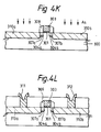
- this structure is made by a sequence of masking and ion implantation steps. The steps involved are illustrated in Figures 4F to 4L herein.
- a semi-fabricated product comprising a P-type substrate 300 with a gate insulating layer 301 of metal oxide formed on its top surface, and a gate 303 built on the gate insulating layer 301 is prepared according to a conventional method.
- Phosphorus ions (1 x 1013cm ⁇ 2; 35 KeV) are injected perpendicular to the top surface of the P-type substrate 300 to form two opposite N-type diffusion layers 304a and 304b of least concentration of phosphorus in the substrate 300. These diffused regions 304a and 304b extend from first and second locations under one and the other edges of the gate 303 respectively in opposite directions.
- a 1000 angstrom-thick oxide layer 305 is formed on the semi-fabricated product (Fig.4F); and the thick oxide layer 305 is subjected to anisotropic etching until the top surface of the substrate 300 is exposed to leave a side wall 306 surrounding the gate 303 (Fig.4G).
- Phosphorus ions (1 x 1014cm ⁇ 2; 35 KeV) are injected perpendicular to the P-type substrate 300 to form two opposite N-type diffusion layers 307a and 307b of less concentration of phosphorus in the substrate 300 (Fig.4H). These diffused regions 307a and 307b extend short of the terminal ends of the diffusion layers 304a and 304b of least concentration of phosphorus.
- a 2000 angstrom-thick oxide layer 308 is then formed on the sidewalled product (Fig.4I); and the thick oxide layer 308 is subjected to anisotropic etching until the top surface of the substrate 300 is exposed to leave a second side wall 309 surrounding the first side wall 306 of the gate 303 (Fig.4J).
- Arsenic ions (5 x 1015cm ⁇ 2; 40 KeV) are injected perpendicular to the P-type substrate 300 to form two opposite diffusion layers 310a and 310b of relatively high concentration of arsenic in the substrate 300 (Fig.4K). These heavily diffused regions 310a and 310b extend from first and second locations under one and the other edges of the second side wall 309 in opposite directions.
- a source electrode 311, a drain electrode 312 and a gate electrode are formed respectively (Fig.4L).
- Japanese patent publication No. JP-A-60136376, as set out in Patent Abstracts of Japan Vol. 9, No.298, describes a further MOSFET having a LDD structure in which the source and drain each comprise three regions of different impurity concentrations. Two regions are initially implanted, using the gate and a subsequently formed side wall as masks, and the third region formed between the first two by a diffusion process.
- VLSI Technology, S.M. Sze, editor, McGraw Hill, 1988, pages 362, 363 describes a process for reducing the depth of an ion-implanted region for a given ion type and ion beam energy by tilting the ion beam direction with respect to the implanted surface. This is to enable a relatively shallow ion-implanted region to be formed using a relatively high beam energy.
- US patent No. 4771012 describes a method of fabricating a FET in which the source and drain are formed by ion implantation using the gate as a mask, the ion beam being tilted to an angle of 7° from a line perpendicular to the substrate surface to avoid channelling in the substrate.
- the substrate is rotated during implantation to eliminate any effects of shadowing of the substrate by the gate and to reduce any resulting asymmetry of the source and drain structures.
- US 4771012 describes the fabrication of a LDD MOSFET having two regions of different impurity concentrations in each of the source and drain.
- the first region in each is formed using the gate as a mask and the second using a subsequently formed side wall as a mask. Both regions are formed using a 7° tilted ion beam.
- the invention provides a method of making a metal-oxide semiconductor field-effect transistor (MOSFET) as defined in claim 1, and a MOSFET structure made by the method of claim 1.
- MOSFET metal-oxide semiconductor field-effect transistor
- a preferred feature of the invention is defined in a subclaim.
- the invention may thus provide an improved method for making a metal-oxide semiconductor field-effect transistor whose structure permits reduction of its size without lowering its current driving capability.
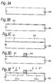
- FIGs.3A to 3J a method of making a MOSFET according to the present invention is described.
- Figs.3A to 3D show how a semi-fabricated product comprising a semiconductor substrate of one conductivity type with a gate insulating layer formed on its top surface, and a gate built on the gate insulating layer can be prepared according to a conventional method.
- a P-type silicon substrate 200 is prepared (Fig.3A); a silicon oxide layer 201 is formed on the top surface of the substrate 200 by heating the substrate 200 in an oxidizing atmosphere (Fig.3B); a polysilicon layer 202 is formed on the silicon oxide layer 201 (Fig.3C); and the polysilicon layer 202 is subjected to anisotropic etching to leave a gate 203 on the silicon oxide layer 201 (Fig.3D).
- a semi-fabricated product results.
- Phosphorus ions (1 x 1013cm ⁇ 2; 40 KeV) are then injected perpendicular to the top surface of the P-type substrate to form two opposite N-type diffusion layers 204a and 204b of least concentration of phosphorus in the substrate 200.
- These diffused regions 204a and 204b extend from first and second locations under one and the other edges of the gate 203 respectively in opposite directions (Fig.3E).
- a 2000 angstrom-thick oxide layer 205 is formed on the semi-fabricated product (Fig.3F); and the thick oxide layer 205 is subjected to anisotropic etching until the top surface of the substrate 200 is exposed to leave a side wall 206 surrounding the gate 203 (Fig.3G).
- Phosphorus ions (5 x 1013cm ⁇ 2; 50 to 60 KeV) are injected to the P-type substrate 200 at 45 degrees to form two opposite N-type diffusion layers 207a and 207b of less, or an intermediate, concentration of phosphorus in the substrate 200 (Fig.3H). These diffused regions 207a and 207b extend short of the terminal ends of the diffusion layers 204a and 204b of least concentration of phosphorus.
- Arsenic ions (5 x 1015cm ⁇ 2; 70 KeV) are injected to the P-type substrate 200 perpendicular to the top surface of the substrate to form two opposite diffusion layers 208a and 208b of relatively high concentration of arsenic in the substrate 200 (Fig.3I). These heavily diffused regions 208a and 208b extend from first and second locations under one and the other edges of the side wall 206 in opposite directions.
- a source electrode 209, a drain electrode 210 and a gate electrode are formed respectively (Fig.3J).
- the two diffused regions 208a and 208b are of the same construction. Conveniently this permits either diffused region to be used as drain when the device is actually used.
- a metal-oxide semiconductor field-effect transistor thus made has two similar diffused regions each extending toward and ending at a location under one or the other edge of the gate 203 in the substrate 200.
- Each is composed of a first relatively short section 204a, 204b of least concentration of impurity, a second relatively short section 207a, 207b of less concentration of impurity, and a third relatively long section 208a, 208b of relatively high concentration of impurity.
- this permits either diffused region to be used as drain when actually the device is used.
Landscapes
- Insulated Gate Type Field-Effect Transistor (AREA)
Claims (2)
- Verfahren zur Herstellung eines Metall-Oxid-Halbleiter-Feldeffekttransistors durch Herstellen eines Halbfertigprodukts mit einem Halbleitersubstrat (200) eines Leitfähigkeitstyps, auf dessen oberer Fläche eine Gate-Isolierschicht (201) ausgebildet ist, und einem auf der Gate-Isolierschicht aufgebauten Gate (203), Ausbilden zweier diffundierter Bereiche des anderen Leitfähigkeitstyps, die sich von unterhalb des einen und des anderen Randes des Gates in entgegengesetzte Richtungen erstrecken, und Ausbilden von Drain-, Source- und Gate-Elektroden, wobei mindestens einer der diffundierten Bereiche durch die folgenden Schritte ausgebildet wird:(A) Injektion von Störstellen des anderen Leitfähigkeitstyps in das Halbleitersubstrat senkrecht zur oberen Fläche des Halbleitersubstrats, um eine Diffusionsschicht (204a, 204b) mit geringster Störstellenkonzentration in dem Halbleitersubstrat auszubilden, die sich von einer Stelle unterhalb eines Randes des Gates aus erstreckt;(B) Ausbilden einer Seitenwand (206), die das Gate auf dem Halbleitersubstrat umgibt; und(C) Injektion von Störstellen des anderen Leitfähigkeitstyps in das Halbleitersubstrat senkrecht zur oberen Fläche des Halbleitersubstrats, um eine Diffusionsschicht (208a, 208b) von relativ hoher Störstellenkonzentration in dem Halbleitersubstrat auszubilden, die sich von einer Stelle unter einem entsprechenden Rand der Seitenwand aus erstreckt;
gekennzeichnet durch den Schritt (D), wobei nach dem Ausbilden der Seitenwand Störstellen des anderen Leitfähigkeitstyps unter einem vorgegebenen spitzen Winkel bezüglich der Flächennormalen zur oberen Fläche des Halbleitersubstrats in das Halbleitersubstrat injiziert werden, um eine Diffusionsschicht (207a, 207b) von geringerer Störstellenkonzentration in dem Halbleitersubstrat auszubilden, die von unterhalb der Seitenwand, kurz vor dem Ende der Diffusionsschicht (204a, 204b) mit geringster Störstellenkonzentration, ausgeht. - Verfahren nach Anspruch 1, wobei beide diffundierten Bereiche gemäß ähnlichen Verfahrensschritten ausgebildet werden, so daß im Schritt (A) zwei einander gegenüberliegende Diffusionsschichten (204a, 204b) von geringster Störstellenkonzentration ausgebildet werden, die sich von einer ersten und einer zweiten Stelle unter dem einen bzw. dem anderen Rand des Gates aus in entgegengesetzte Richtungen erstrecken, während im Schritt (C) zwei einander gegenüberliegende Diffusionsschichten (208a, 208b) von relativ hoher Störstellenkonzentration ausgebildet werden, die sich von einer ersten und einer zweiten Stelle unter dem einen bzw. dem anderen Rand der Seitenwand aus in entgegengesetzte Richtungen erstrecken, und im Schritt (D) zwei einander gegenüberliegende Diffusionsschichten (207a, 207b) von geringerer Störstellenkonzentration ausgebildet werden, die von Stellen kurz vor den Enden der Diffusionsschichten (204a, 204b) mit geringster Störstellenkonzentration ausgehen.
Applications Claiming Priority (2)
| Application Number | Priority Date | Filing Date | Title |
|---|---|---|---|
| JP339394/90 | 1990-11-30 | ||
| JP2339394A JPH04206933A (ja) | 1990-11-30 | 1990-11-30 | 半導体装置 |
Publications (2)
| Publication Number | Publication Date |
|---|---|
| EP0489559A1 EP0489559A1 (de) | 1992-06-10 |
| EP0489559B1 true EP0489559B1 (de) | 1995-07-12 |
Family
ID=18327060
Family Applications (1)
| Application Number | Title | Priority Date | Filing Date |
|---|---|---|---|
| EP91311183A Expired - Lifetime EP0489559B1 (de) | 1990-11-30 | 1991-12-02 | LDD Metalloxyd-Halbleiter-Feldeffekttransistor und Verfahren zur Herstellung |
Country Status (4)
| Country | Link |
|---|---|
| US (1) | US5292674A (de) |
| EP (1) | EP0489559B1 (de) |
| JP (1) | JPH04206933A (de) |
| DE (1) | DE69111203T2 (de) |
Families Citing this family (7)
| Publication number | Priority date | Publication date | Assignee | Title |
|---|---|---|---|---|
| US5376566A (en) * | 1993-11-12 | 1994-12-27 | Micron Semiconductor, Inc. | N-channel field effect transistor having an oblique arsenic implant for lowered series resistance |
| US5439835A (en) * | 1993-11-12 | 1995-08-08 | Micron Semiconductor, Inc. | Process for DRAM incorporating a high-energy, oblique P-type implant for both field isolation and punchthrough |
| US5614432A (en) * | 1994-04-23 | 1997-03-25 | Nec Corporation | Method for manufacturing LDD type MIS device |
| US5478763A (en) * | 1995-01-19 | 1995-12-26 | United Microelectronics Corporation | High performance field effect transistor and method of manufacture thereof |
| US5935867A (en) * | 1995-06-07 | 1999-08-10 | Advanced Micro Devices, Inc. | Shallow drain extension formation by angled implantation |
| US6180470B1 (en) * | 1996-12-19 | 2001-01-30 | Lsi Logic Corporation | FETs having lightly doped drain regions that are shaped with counter and noncounter dorant elements |
| WO1998032176A1 (en) * | 1997-01-21 | 1998-07-23 | Advanced Micro Devices, Inc. | As/P HYBRID nLDD JUNCTION AND MEDIUM Vdd OPERATION FOR HIGH SPEED MICROPROCESSORS |
Family Cites Families (15)
| Publication number | Priority date | Publication date | Assignee | Title |
|---|---|---|---|---|
| JPS60136376A (ja) * | 1983-12-26 | 1985-07-19 | Hitachi Ltd | 半導体装置の製造方法 |
| EP0187016B1 (de) * | 1984-12-27 | 1991-02-20 | Kabushiki Kaisha Toshiba | MISFET mit niedrigdotiertem Drain und Verfahren zu seiner Herstellung |
| JPS61216364A (ja) * | 1985-03-20 | 1986-09-26 | Fujitsu Ltd | 半導体装置 |
| JPS62113474A (ja) * | 1985-11-13 | 1987-05-25 | Toshiba Corp | 半導体集積回路の製造方法 |
| JPH0789587B2 (ja) * | 1985-12-27 | 1995-09-27 | 株式会社東芝 | 絶縁ゲート型電界効果トランジスタおよびその製造方法 |
| US4771012A (en) * | 1986-06-13 | 1988-09-13 | Matsushita Electric Industrial Co., Ltd. | Method of making symmetrically controlled implanted regions using rotational angle of the substrate |
| US4746624A (en) * | 1986-10-31 | 1988-05-24 | Hewlett-Packard Company | Method for making an LDD MOSFET with a shifted buried layer and a blocking region |
| US4835740A (en) * | 1986-12-26 | 1989-05-30 | Kabushiki Kaisha Toshiba | Floating gate type semiconductor memory device |
| US5061975A (en) * | 1988-02-19 | 1991-10-29 | Mitsubishi Denki Kabushiki Kaisha | MOS type field effect transistor having LDD structure |
| JP2562688B2 (ja) * | 1989-05-12 | 1996-12-11 | 三洋電機株式会社 | 半導体装置の製造方法 |
| US5158903A (en) * | 1989-11-01 | 1992-10-27 | Matsushita Electric Industrial Co., Ltd. | Method for producing a field-effect type semiconductor device |
| US5023190A (en) * | 1990-08-03 | 1991-06-11 | Micron Technology, Inc. | CMOS processes |
| US5091763A (en) * | 1990-12-19 | 1992-02-25 | Intel Corporation | Self-aligned overlap MOSFET and method of fabrication |
| US5102815A (en) * | 1990-12-19 | 1992-04-07 | Intel Corporation | Method of fabricating a composite inverse T-gate metal oxide semiconductor device |
| US5162884A (en) * | 1991-03-27 | 1992-11-10 | Sgs-Thomson Microelectronics, Inc. | Insulated gate field-effect transistor with gate-drain overlap and method of making the same |
-
1990
- 1990-11-30 JP JP2339394A patent/JPH04206933A/ja active Pending
-
1991
- 1991-11-29 US US07/800,170 patent/US5292674A/en not_active Expired - Fee Related
- 1991-12-02 DE DE69111203T patent/DE69111203T2/de not_active Expired - Fee Related
- 1991-12-02 EP EP91311183A patent/EP0489559B1/de not_active Expired - Lifetime
Also Published As
| Publication number | Publication date |
|---|---|
| DE69111203D1 (de) | 1995-08-17 |
| EP0489559A1 (de) | 1992-06-10 |
| DE69111203T2 (de) | 1996-04-04 |
| JPH04206933A (ja) | 1992-07-28 |
| US5292674A (en) | 1994-03-08 |
Similar Documents
| Publication | Publication Date | Title |
|---|---|---|
| US6023088A (en) | Semiconductor device formed on an insulator and having a damaged portion at the interface between the insulator and the active layer | |
| EP0696054B1 (de) | Verfahren zur Herstellung von Leistungsbauteilen hoher Dichte in MOS-Technologie | |
| JP3528420B2 (ja) | 半導体装置およびその製造方法 | |
| US5016067A (en) | Vertical MOS transistor | |
| KR910002037B1 (ko) | 반도체장치 및 그 제조방법 | |
| JP2000183348A (ja) | Mosゲ―ト電力装置 | |
| KR100374551B1 (ko) | 반도체 소자 및 그 제조방법 | |
| US6238985B1 (en) | Semiconductor device and method for fabricating the same | |
| JPH09116153A (ja) | 半導体装置 | |
| US6963109B2 (en) | Semiconductor device and method for manufacturing the same | |
| US5386133A (en) | LDD FET with polysilicon sidewalls | |
| US6020611A (en) | Semiconductor component and method of manufacture | |
| KR0180310B1 (ko) | 상보형 모스 트랜지스터 및 그 제조방법 | |
| US6261910B1 (en) | Semiconductor device and method of manufacturing the same | |
| EP0489559B1 (de) | LDD Metalloxyd-Halbleiter-Feldeffekttransistor und Verfahren zur Herstellung | |
| US6025239A (en) | Method for fabricating an electrostatic discharge device | |
| KR100291405B1 (ko) | 필드산화물전계효과트랜지스터및그제조방법 | |
| JP2924947B2 (ja) | 半導体装置の製造方法 | |
| JPH06224216A (ja) | トランジスター及びその製造方法 | |
| JPH10144922A (ja) | 電界効果トランジスタ(fet)および半導体電界効果トランジスタを形成する方法 | |
| US6215153B1 (en) | MOSFET and method for fabricating the same | |
| KR0175367B1 (ko) | 반도체 장치 및 그 제조 방법 | |
| US6057191A (en) | Process for the fabrication of integrated circuits with contacts self-aligned to active areas | |
| JPH0555583A (ja) | 絶縁ゲート型バイポーラトランジスタの製造方法 | |
| JP3061157B2 (ja) | 半導体素子の形成方法 |
Legal Events
| Date | Code | Title | Description |
|---|---|---|---|
| PUAI | Public reference made under article 153(3) epc to a published international application that has entered the european phase |
Free format text: ORIGINAL CODE: 0009012 |
|
| 17P | Request for examination filed |
Effective date: 19911217 |
|
| AK | Designated contracting states |
Kind code of ref document: A1 Designated state(s): DE FR GB |
|
| 17Q | First examination report despatched |
Effective date: 19940214 |
|
| GRAA | (expected) grant |
Free format text: ORIGINAL CODE: 0009210 |
|
| AK | Designated contracting states |
Kind code of ref document: B1 Designated state(s): DE FR GB |
|
| REF | Corresponds to: |
Ref document number: 69111203 Country of ref document: DE Date of ref document: 19950817 |
|
| ET | Fr: translation filed | ||
| PGFP | Annual fee paid to national office [announced via postgrant information from national office to epo] |
Ref country code: GB Payment date: 19951130 Year of fee payment: 5 |
|
| PGFP | Annual fee paid to national office [announced via postgrant information from national office to epo] |
Ref country code: FR Payment date: 19951218 Year of fee payment: 5 |
|
| PGFP | Annual fee paid to national office [announced via postgrant information from national office to epo] |
Ref country code: DE Payment date: 19960228 Year of fee payment: 5 |
|
| PLBE | No opposition filed within time limit |
Free format text: ORIGINAL CODE: 0009261 |
|
| STAA | Information on the status of an ep patent application or granted ep patent |
Free format text: STATUS: NO OPPOSITION FILED WITHIN TIME LIMIT |
|
| 26N | No opposition filed | ||
| PG25 | Lapsed in a contracting state [announced via postgrant information from national office to epo] |
Ref country code: GB Effective date: 19961202 |
|
| GBPC | Gb: european patent ceased through non-payment of renewal fee |
Effective date: 19961202 |
|
| PG25 | Lapsed in a contracting state [announced via postgrant information from national office to epo] |
Ref country code: FR Effective date: 19970829 |
|
| PG25 | Lapsed in a contracting state [announced via postgrant information from national office to epo] |
Ref country code: DE Effective date: 19970902 |
|
| REG | Reference to a national code |
Ref country code: FR Ref legal event code: ST |