EP0504473B1 - Magnetische Mehrschicht und Element mit Magnetowiderstandseffekt - Google Patents
Magnetische Mehrschicht und Element mit Magnetowiderstandseffekt Download PDFInfo
- Publication number
- EP0504473B1 EP0504473B1 EP91113878A EP91113878A EP0504473B1 EP 0504473 B1 EP0504473 B1 EP 0504473B1 EP 91113878 A EP91113878 A EP 91113878A EP 91113878 A EP91113878 A EP 91113878A EP 0504473 B1 EP0504473 B1 EP 0504473B1
- Authority
- EP
- European Patent Office
- Prior art keywords
- magnetic
- multilayer
- film
- magnetic field
- films
- Prior art date
- Legal status (The legal status is an assumption and is not a legal conclusion. Google has not performed a legal analysis and makes no representation as to the accuracy of the status listed.)
- Expired - Lifetime
Links
- 230000005291 magnetic effect Effects 0.000 title claims description 143
- 230000000694 effects Effects 0.000 title claims description 8
- 239000000758 substrate Substances 0.000 claims description 36
- 230000005415 magnetization Effects 0.000 claims description 30
- 239000010409 thin film Substances 0.000 claims description 28
- 230000005303 antiferromagnetism Effects 0.000 claims description 18
- 238000000034 method Methods 0.000 claims description 12
- 229910052759 nickel Inorganic materials 0.000 claims description 8
- 230000001747 exhibiting effect Effects 0.000 claims description 3
- 239000010408 film Substances 0.000 description 61
- 230000008859 change Effects 0.000 description 48
- CPLXHLVBOLITMK-UHFFFAOYSA-N Magnesium oxide Chemical compound [Mg]=O CPLXHLVBOLITMK-UHFFFAOYSA-N 0.000 description 20
- 239000011521 glass Substances 0.000 description 15
- 239000000395 magnesium oxide Substances 0.000 description 11
- 230000008878 coupling Effects 0.000 description 10
- 238000010168 coupling process Methods 0.000 description 10
- 238000005859 coupling reaction Methods 0.000 description 10
- XEEYBQQBJWHFJM-UHFFFAOYSA-N iron Substances [Fe] XEEYBQQBJWHFJM-UHFFFAOYSA-N 0.000 description 10
- 230000005290 antiferromagnetic effect Effects 0.000 description 7
- 238000002441 X-ray diffraction Methods 0.000 description 5
- 229910045601 alloy Inorganic materials 0.000 description 4
- 239000000956 alloy Substances 0.000 description 4
- 230000015572 biosynthetic process Effects 0.000 description 4
- 238000000151 deposition Methods 0.000 description 4
- 229910052742 iron Inorganic materials 0.000 description 4
- 239000000463 material Substances 0.000 description 4
- 229910052751 metal Inorganic materials 0.000 description 4
- 239000002184 metal Substances 0.000 description 4
- 230000003534 oscillatory effect Effects 0.000 description 4
- 230000000052 comparative effect Effects 0.000 description 3
- 239000002245 particle Substances 0.000 description 3
- 230000000737 periodic effect Effects 0.000 description 3
- 238000004544 sputter deposition Methods 0.000 description 3
- 229910001030 Iron–nickel alloy Inorganic materials 0.000 description 2
- 229910017709 Ni Co Inorganic materials 0.000 description 2
- 229910003267 Ni-Co Inorganic materials 0.000 description 2
- 229910003262 Ni‐Co Inorganic materials 0.000 description 2
- 230000005540 biological transmission Effects 0.000 description 2
- 229910052804 chromium Inorganic materials 0.000 description 2
- 239000013078 crystal Substances 0.000 description 2
- 238000010586 diagram Methods 0.000 description 2
- AXZKOIWUVFPNLO-UHFFFAOYSA-N magnesium;oxygen(2-) Chemical compound [O-2].[Mg+2] AXZKOIWUVFPNLO-UHFFFAOYSA-N 0.000 description 2
- 230000005381 magnetic domain Effects 0.000 description 2
- 230000005389 magnetism Effects 0.000 description 2
- 238000005259 measurement Methods 0.000 description 2
- 238000001451 molecular beam epitaxy Methods 0.000 description 2
- 238000001683 neutron diffraction Methods 0.000 description 2
- 239000000700 radioactive tracer Substances 0.000 description 2
- 238000012552 review Methods 0.000 description 2
- 229910052709 silver Inorganic materials 0.000 description 2
- 238000001771 vacuum deposition Methods 0.000 description 2
- JBRZTFJDHDCESZ-UHFFFAOYSA-N AsGa Chemical compound [As]#[Ga] JBRZTFJDHDCESZ-UHFFFAOYSA-N 0.000 description 1
- 229910001218 Gallium arsenide Inorganic materials 0.000 description 1
- 230000005374 Kerr effect Effects 0.000 description 1
- 229910052581 Si3N4 Inorganic materials 0.000 description 1
- VYPSYNLAJGMNEJ-UHFFFAOYSA-N Silicium dioxide Chemical compound O=[Si]=O VYPSYNLAJGMNEJ-UHFFFAOYSA-N 0.000 description 1
- XUIMIQQOPSSXEZ-UHFFFAOYSA-N Silicon Chemical compound [Si] XUIMIQQOPSSXEZ-UHFFFAOYSA-N 0.000 description 1
- 238000004458 analytical method Methods 0.000 description 1
- 230000003064 anti-oxidating effect Effects 0.000 description 1
- JRPBQTZRNDNNOP-UHFFFAOYSA-N barium titanate Chemical compound [Ba+2].[Ba+2].[O-][Ti]([O-])([O-])[O-] JRPBQTZRNDNNOP-UHFFFAOYSA-N 0.000 description 1
- 229910002113 barium titanate Inorganic materials 0.000 description 1
- 230000008901 benefit Effects 0.000 description 1
- AOWKSNWVBZGMTJ-UHFFFAOYSA-N calcium titanate Chemical compound [Ca+2].[O-][Ti]([O-])=O AOWKSNWVBZGMTJ-UHFFFAOYSA-N 0.000 description 1
- 238000011109 contamination Methods 0.000 description 1
- 230000001419 dependent effect Effects 0.000 description 1
- 230000008021 deposition Effects 0.000 description 1
- 238000013461 design Methods 0.000 description 1
- 238000005516 engineering process Methods 0.000 description 1
- 230000005294 ferromagnetic effect Effects 0.000 description 1
- 230000005307 ferromagnetism Effects 0.000 description 1
- 239000003574 free electron Substances 0.000 description 1
- 238000010438 heat treatment Methods 0.000 description 1
- 230000006872 improvement Effects 0.000 description 1
- 238000003475 lamination Methods 0.000 description 1
- GQYHUHYESMUTHG-UHFFFAOYSA-N lithium niobate Chemical compound [Li+].[O-][Nb](=O)=O GQYHUHYESMUTHG-UHFFFAOYSA-N 0.000 description 1
- 238000004519 manufacturing process Methods 0.000 description 1
- 150000002739 metals Chemical class 0.000 description 1
- 239000000203 mixture Substances 0.000 description 1
- 230000010355 oscillation Effects 0.000 description 1
- 229910000889 permalloy Inorganic materials 0.000 description 1
- 230000008569 process Effects 0.000 description 1
- 238000002128 reflection high energy electron diffraction Methods 0.000 description 1
- 238000011160 research Methods 0.000 description 1
- 238000010079 rubber tapping Methods 0.000 description 1
- 229910052594 sapphire Inorganic materials 0.000 description 1
- 239000010980 sapphire Substances 0.000 description 1
- 229920006395 saturated elastomer Polymers 0.000 description 1
- 238000000682 scanning probe acoustic microscopy Methods 0.000 description 1
- 229910052710 silicon Inorganic materials 0.000 description 1
- 239000010703 silicon Substances 0.000 description 1
- HQVNEWCFYHHQES-UHFFFAOYSA-N silicon nitride Chemical compound N12[Si]34N5[Si]62N3[Si]51N64 HQVNEWCFYHHQES-UHFFFAOYSA-N 0.000 description 1
- 229910052814 silicon oxide Inorganic materials 0.000 description 1
- 238000001988 small-angle X-ray diffraction Methods 0.000 description 1
- 239000007787 solid Substances 0.000 description 1
- VEALVRVVWBQVSL-UHFFFAOYSA-N strontium titanate Chemical compound [Sr+2].[O-][Ti]([O-])=O VEALVRVVWBQVSL-UHFFFAOYSA-N 0.000 description 1
- 239000000126 substance Substances 0.000 description 1
- 239000013589 supplement Substances 0.000 description 1
Images


Classifications
-
- G—PHYSICS
- G01—MEASURING; TESTING
- G01R—MEASURING ELECTRIC VARIABLES; MEASURING MAGNETIC VARIABLES
- G01R33/00—Arrangements or instruments for measuring magnetic variables
- G01R33/02—Measuring direction or magnitude of magnetic fields or magnetic flux
- G01R33/06—Measuring direction or magnitude of magnetic fields or magnetic flux using galvano-magnetic devices
- G01R33/09—Magnetoresistive devices
- G01R33/093—Magnetoresistive devices using multilayer structures, e.g. giant magnetoresistance sensors
-
- B—PERFORMING OPERATIONS; TRANSPORTING
- B82—NANOTECHNOLOGY
- B82Y—SPECIFIC USES OR APPLICATIONS OF NANOSTRUCTURES; MEASUREMENT OR ANALYSIS OF NANOSTRUCTURES; MANUFACTURE OR TREATMENT OF NANOSTRUCTURES
- B82Y25/00—Nanomagnetism, e.g. magnetoimpedance, anisotropic magnetoresistance, giant magnetoresistance or tunneling magnetoresistance
-
- H—ELECTRICITY
- H01—ELECTRIC ELEMENTS
- H01F—MAGNETS; INDUCTANCES; TRANSFORMERS; SELECTION OF MATERIALS FOR THEIR MAGNETIC PROPERTIES
- H01F10/00—Thin magnetic films, e.g. of one-domain structure
- H01F10/32—Spin-exchange-coupled multilayers, e.g. nanostructured superlattices
- H01F10/324—Exchange coupling of magnetic film pairs via a very thin non-magnetic spacer, e.g. by exchange with conduction electrons of the spacer
- H01F10/325—Exchange coupling of magnetic film pairs via a very thin non-magnetic spacer, e.g. by exchange with conduction electrons of the spacer the spacer being noble metal
-
- H—ELECTRICITY
- H10—SEMICONDUCTOR DEVICES; ELECTRIC SOLID-STATE DEVICES NOT OTHERWISE PROVIDED FOR
- H10N—ELECTRIC SOLID-STATE DEVICES NOT OTHERWISE PROVIDED FOR
- H10N50/00—Galvanomagnetic devices
- H10N50/80—Constructional details
- H10N50/85—Materials of the active region
-
- Y—GENERAL TAGGING OF NEW TECHNOLOGICAL DEVELOPMENTS; GENERAL TAGGING OF CROSS-SECTIONAL TECHNOLOGIES SPANNING OVER SEVERAL SECTIONS OF THE IPC; TECHNICAL SUBJECTS COVERED BY FORMER USPC CROSS-REFERENCE ART COLLECTIONS [XRACs] AND DIGESTS
- Y10—TECHNICAL SUBJECTS COVERED BY FORMER USPC
- Y10S—TECHNICAL SUBJECTS COVERED BY FORMER USPC CROSS-REFERENCE ART COLLECTIONS [XRACs] AND DIGESTS
- Y10S428/00—Stock material or miscellaneous articles
- Y10S428/922—Static electricity metal bleed-off metallic stock
- Y10S428/9265—Special properties
- Y10S428/928—Magnetic property
-
- Y—GENERAL TAGGING OF NEW TECHNOLOGICAL DEVELOPMENTS; GENERAL TAGGING OF CROSS-SECTIONAL TECHNOLOGIES SPANNING OVER SEVERAL SECTIONS OF THE IPC; TECHNICAL SUBJECTS COVERED BY FORMER USPC CROSS-REFERENCE ART COLLECTIONS [XRACs] AND DIGESTS
- Y10—TECHNICAL SUBJECTS COVERED BY FORMER USPC
- Y10T—TECHNICAL SUBJECTS COVERED BY FORMER US CLASSIFICATION
- Y10T428/00—Stock material or miscellaneous articles
- Y10T428/12—All metal or with adjacent metals
- Y10T428/12465—All metal or with adjacent metals having magnetic properties, or preformed fiber orientation coordinate with shape
-
- Y—GENERAL TAGGING OF NEW TECHNOLOGICAL DEVELOPMENTS; GENERAL TAGGING OF CROSS-SECTIONAL TECHNOLOGIES SPANNING OVER SEVERAL SECTIONS OF THE IPC; TECHNICAL SUBJECTS COVERED BY FORMER USPC CROSS-REFERENCE ART COLLECTIONS [XRACs] AND DIGESTS
- Y10—TECHNICAL SUBJECTS COVERED BY FORMER USPC
- Y10T—TECHNICAL SUBJECTS COVERED BY FORMER US CLASSIFICATION
- Y10T428/00—Stock material or miscellaneous articles
- Y10T428/12—All metal or with adjacent metals
- Y10T428/12493—Composite; i.e., plural, adjacent, spatially distinct metal components [e.g., layers, joint, etc.]
- Y10T428/12632—Four or more distinct components with alternate recurrence of each type component
Definitions
- This invention relates to a magnetic multilayer structure and a magnetoresistance effect element (MR element) using the same.
- MRelements including various magnetic sensors (MR sensors) and magnetic heads (MR heads) are to detect a change in electric resistance produced in a magnetic film on application of a magnetic field to thereby measure the magnetic field intensity or its change. They are generally required to have a great differential magnetoresistance and a low operating magnetic field intensity at room temperature.
- Prior art MR elements used magnetic films of Fe-Ni (Permalloy) and Ni-Co alloys in order to take advantage of their anisotropic magnetoresistance effect.
- the Fe-Ni and Ni-Co alloys can operate with a low magnetic field intensity, but have a differential magnetoresistance as low as 2 to 5%.
- Each artificial superlattice has a multilayered structure including thin metal layers having a thickness of an atomic order stacked at regular intervals using a molecular beam epitaxial (MBE) method and exhibits different properties from bulk metal.
- MBE molecular beam epitaxial
- One of recently developed artificial superlattices is a giant magnetoresistance changing material in the form of an Fe/Cr magnetic multilayer comprising alternately stacked Fe and Cr films.
- this multilayer a pair of Fe films sandwiching a Cr film are magnetically coupled in antiparallelism.
- Fe spins are gradually aligned in one given direction and accordingly, the resistance lowers.
- the multilayer shows a giant magnetoresistance change of 46% at 4.2K and 16% at room temperature (see Physical Review Letters, Vol. 61, page 2472, 1988).
- the Fe/Cr magnetic multilayer has such a giant magnetoresistance change, but requires an operating magnetic field intensity of about 1592 (20 kOe), which im- poses some limitations on the multilayer in practical use.
- a primary object of the present invention is to provide a novel and improved magnetic multilayer having a giant magnetoresistance change and requiring a low operating magnetic field intensity to provide such a giant magneto-resistance change.
- Another object of the present invention is to provide a novel and improved magnetic multilayer capable of varying the operating magnetic field intensity at which a giant magnetoresistance change is available.
- Afurther.object of the present invention is to provide a magnetoresistance effect element using such a magnetic multilayer.
- a magnetic multilayer on a substrate comprising at least one magnetic thin film containing at least one member selected from the group consisting of Co and Ni as well as at least one Ag thin film stacked one on top of another is provided, whereby said multilayer shows an axis of easy magnetization in a plane parallel to the surface and a squareness ratio Br/Bs in the plane of up to 0.5.
- the multilayer is defined as exhibiting antiferromagnetism.
- the magnetic thin films and the Ag thin films are formed by a molecular beam epitaxial method.
- the magnetic thin films have a thickness of 2 to 60 x 10- 10 m (2 to 60 A)
- the Ag thin films have a thickness of 2 to 60 x 10-' O m (2 to 60 A).
- magnetoresistance effect element comprising a magnetic multilayer as defined above.
- Journal of Japan Applied Magnetism Society, 13,339-342 (1989) discloses an artificial lattice magnetic multilayer of Co/Au system using a molecular beam epitaxial method.
- This multilayer has vertical magnetic anisotropy and a magnetoresistance change as low as 1% at 39.6 (0.5 kOe)and room temperature.
- the magnetic multilayer of the present invention includes a plurality of magnetic thin films containing an iron group element and a plurality of non-magnetic intervening layers in the form of Ag thin films on a substrate.
- the magnetic thin films and Ag thin films are alternately stacked on the substrate.
- Each of the magnetic thin films contains at least one element selected from Co and Ni.
- the magnetic film is preferably formed of Co or Ni alone or an alloy of Co and Ni. It is also acceptable to form the magnetic film from an alloy containing at least 30 at% of Co, Ni or a mixture of two of them.
- the magnetic film preferably has a thickness of up to 60 x 10- 10 m (60 A), more preferably up to 50 x 10- 10 m (50 A), especially up to 40 x 10- 10 m (40 A), most preferably up to 20 x 10- 10 m (20 A). In excess of 60 x 10- 10 m (60 A) in thickness, a giant magnetoresistance change would not be available since magnetic elements in adjacent films would be spaced a relatively large enough distance to cancel antiferromagnetic coupling.
- the magnetic film should preferably be at least 2 x 10⁻¹ Om (2 A), more preferably at least 4 x 10- 10 m (4 A) thick. In a film of less than 2 x 10- 10 m (2 A) thick, magnetic elements would not be continuously and closely arranged in the plane of formation, resulting in a loss of ferromagnetism.
- Each of the Ag thin films is a film consisting essentially of Ag, preferably a film consisting solely of Ag.
- the Ag film preferably has a thickness of up to 60 x 10- 10 m (60 A), more preferably up to 50 x 10- 10 m (50 A), most preferably up to 45 x 10- 10 m (45 A). If the intervening Ag film is more than 60 x 10- 10 m (60 A) thick, magnetic films would be spaced a relatively large distance so that antiferromagnetic coupling would be lost.
- the Ag film should preferably be at least 2 ⁇ 10- 10 m (2 A) thick. If the Ag film is less than 2 ⁇ 10- 10 m (2 A) thick, it cannot be continuous with its function as a nonmagnetic intervening layer lost.
- the magnetic exchange coupling energy periodically oscillates and varies with the repetition interval of the magnetic layers, typically a change in the thickness of the Ag films.
- oscillatory magnetic exchange coupling mainly depends on the thickness of Ag thin films.
- the thickness of Ag thin films is varied over the range of from 2 to 60 x 10- 10 m (2 to 60 A)
- saturation magnetic field applied, Hsat varies periodically in the range of from 79.6 to 796 kA/m (1 to 10 kOe).
- the maximum and minimum of Hsat also vary.
- the magnetoresistance change varies and oscillates periodically.
- the thickness of the Ag films in the range of 2 to 60 x 10-"'m (2 to 60 A), there is obtained freedom of design for magnetic multilayers having a magnetoresistance change of 1 to 20% at room temperature in an operating magnetic field of 0.79 to 1592 (0.01 to 20 kOe) in intensity.
- the thickness of the magnetic thin films and Ag thin films can be measured by means of a transmission or scanning electron microscope and Auger electron spectroscopy and the grain structure can be identified by X-ray diffraction and reflection high energy electron diffraction (RHEED).
- the number of magnetic films stacked and the number of recurring magnetic film/Ag film units are not particularly limited and may be suitably chosen for the desired magnetoresistance change and the like.
- the number of recurring units is 2 or more, more preferably 8 or more in order to provide an acceptable magnetoresistance change.
- a larger number of recurring units is preferred because a more proportion of free electrons are subject to scattering.
- an extremely increased number of recurring units often results in deteriorated film quality and no further property improvement.
- the maximum number of recurring units is preferably limited to 500, especially 200. It is to be noted that a long period superlattice structure can be identified by taking a small angle X-ray diffraction pattern where primary and secondary peaks corresponding to recurring periodicities appear.
- the magnetic multilayer of the invention exhibits antiferromagnetism.
- the antiferromagnetism can be readily identified by polarized neutron diffraction, for example.
- the multilayer has a squareness ratio Br/Bs of up to 0.5, especially up to 0.3, and even approaching zero when a magnetization versus applied magnetic field curve or B-H loop of the multilayer is measured in a plane parallel to its surface by means of a vibrating sample magnetometer (VSM) or B-H tracer.
- VSM vibrating sample magnetometer
- the magnetization versus applied magnetic field curve or B-H loop has closely spaced magnetizing and demagnetizing curve segments.
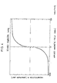
- FIG. 3 shows magnetization versus applied magnetic field curves A and B in planes parallel and normal to the multilayer surface. If Br/Bs in the parallel plane exceeds 0.5, the multilayer would be subject to a drastic drop in the proportion of antiferromagnetism within its interior and a lowering of magnetoresistance change therewith.
- the substrate on which the multilayer is formed may be formed of any desired materials including amorphous glass substrates and crystalline glass substrates as well as other commonly used substrates, for example, single crystal substrates of various oxides such as magnesium oxide, sapphire, silicon, gallium-arsenide, strontium titanate, barium titanate, and lithium niobate and polycrystalline substrates such as alumina-titanium carbide and calcium titanate.
- amorphous glass substrates and crystalline glass substrates as well as other commonly used substrates, for example, single crystal substrates of various oxides such as magnesium oxide, sapphire, silicon, gallium-arsenide, strontium titanate, barium titanate, and lithium niobate and polycrystalline substrates such as alumina-titanium carbide and calcium titanate.
- oxides such as magnesium oxide, sapphire, silicon, gallium-arsenide, strontium titanate, barium titanate, and lithium niobate
- polycrystalline substrates such
- Awide angle X-ray diffraction analysis shows that on a glass substrate, an Ag film has (111) orientation and a Co film has hcp(002) overlapping fcc(111) indicating polycrystalline nature.
- Ag (200) and Co fcc(200) peaks are observed, indicating predominant (100) epitaxial growth.
- the substrate As to the dimensions of the substrate, no limit is imposed and a choice may be made in accordance with a particular element to which the multilayer is to be applied.
- the surface of the substrate on which the magnetic multilayer is to be formed may be provided with an undercoat if desired.
- an antioxidizing film of silicon nitride, silicon oxide, or other metals as well as a conductive metal layer for electrode tapping.
- the magnetic multilayer is preferably prepared by a molecular beam epitaxy (MBE) method. Since the magnetic films and Ag films are very thin, it is necessary to slowly deposit them. Film formation in a ultrahigh vacuum environment is necessary in order to avoid film contamination. In forming respective layers, depositing particles should have as low energy as possible for preventing interdiffusion from occurring with an attendant loss of antiferromagnetism. Best suited for these considerations is an MBE method.
- the MBE method is a kind of ultra high vacuum deposition process causing molecules or substance evaporated from a source in ultrahigh vacuum to deposit on a substrate surface, thereby growing a film.
- sources of magnetic and nonmagnetic materials are equipped with shutters. One of the two sources is selected by opening one shutter with the other shutter closed. Film thickness is monitored by means of a suitable film gauge. In this way, magnetic and nonmagnetic films are alternately deposited.
- the ultimate pressure is generally about 133.3 x 10- 11 to 133.3 x 10- 9 Pa (10- 11 to 10- 9 Torr), and the materials are deposited under a pressure at about 133.3 x 10- 11 to 133.3 x 10- 7 Pa (10- 11 to 10- 7 Torr), especially about 133.3 x 10- 10 to 133.3 x 10 7 Pa (10- 10 to 10- 7 Torr) at a rate of about 0.01 to 10 x 10- 10 m/sec (0.01 to 10 A/sec), especially about 0.1 to 1 ⁇ 10- 10 m/sec (0.1 to 1.0 ⁇ /sec).
- the depositing particles will have a kinetic energy of 0.01 to 5 eV, preferably 0.01 to 1 eV, with its center energy ranging from 0.05 to 0.5 eV.
- the substrate may be heated if desired to obtain films of sound grain structure.
- the heating temperature should preferably be up to 800°C in order to prevent interdiffusion between adjoining films. It is also possible to form magnetic films in a magnetic field to enhance in-plane magnetic anisotropy.
- the magnetic multilayers of the invention are advantageously applicable to various MR elements including MR sensors and MR heads. On use, a biasing magnetic field is applied thereacross if needed. Also, the magnetic multilayers of the invention may be positioned in the gaps or tracks of a thin film type magnetic head so that reading operation can be conducted through the MR strips.
- a vacuum chamber having an ultimate pressure of 933 x 10- 11 Pa (7 ⁇ 10 -11 Torr) was used.
- Film deposition was conducted in an operating pressure of 1293 x 10 -10 Pa (9.7 ⁇ 10 -10 Torr) and at a rate of about 0.5 x 10 -10 m/sec (0.5 A/sec) while the substrate was rotated 30 r.p.m. and heated at 100°C.
- Depositing particles had a central kinetic energy of about 0.1 eV.
- a magnetization versus applied magnetic field curve was measured by means of a vibrating sample magnetometer (VSM). Separately, the sample was cut into a strip of 0.3 mm x 1.0 mm 2 , which was measured for resistivity by a DC four terminal method while the external magnetic field was varied from -1592 to +1592 kA/m (-20 kOe to +20 kOe) at the maximum, for determining a magnetoresistance (MR) change rate AR/R.
- MR magnetoresistance
- AR/R magnetoresistance
- FIG. 1 shows a magnetoresistance change AR/R relative to the applied field.
- Curve labeled Trans is the result obtained when an external magnetic field is applied in the sample plane and transverse to the current flow.
- Curve labeled Long is the result obtained when an external magnetic field is applied in the sample plane and parallel to the current flow.
- Curve labeled Norm is the result obtained when an external magnetic field is applied normal to the sample plane.
- the magnetoresistance change was 13.3% in an applied field of 398 (5 kOe) and 11.2% in an applied field of 238.8 kA/m (3 kOe) both at room temperature.
- curve A A magnetization versus applied magnetic field curve with the field applied in a sample in-plane direction is shown in FIG. 3 as curve A and in FIG. 4.
- the squareness ratio was 0.1.
- curve B in FIG. 3 is a magnetization versus applied magnetic field curve with the field applied in a normal plane.
- the multilayer had an axis of easy magnetization within a plane parallel to the surface, a reduced squareness ratio, and antiferromagnetism.
- polarential neutron diffraction analysis also showed a diffraction line at a Bragg angle corresponding to twice the interval of the multilayer unit thickness, confirming interlaminar antiferromagnetic coupling.
- a magnetic multilayer [Co(6)-Ag(8)]x70 was fabricated by repeating the procedure of Example 1 except that an amorphous glass substrate was used instead.
- This multilayer also had an axis of easy magnetization within a plane parallel to the surface, a squareness ratio Br/Bs of 0.1, and antiferromagnetism.
- the magnetoresistance change AR/R was 8.3% in an applied field of 557.2 (7 kOe) at room tem- perature and 19.4% in an applied field of 1592 (20 kOe) at -196°C (77K).
- Example 1 a magnetic multilayer [Co(10)-Ag(8)]x40 was fabricated on a magnesia substrate.
- the operating pressure was 1053 x 10 -10 Pa (7.9x10- 10 Torr).
- This multilayer also had an axis of easy magnetization within a plane parallel to the surface, a squareness ratio Br/Bs of 0.25, and antiferromagnetism.
- the magnetoresistance change ⁇ R/R was 14.3% in an applied field of 557.2 kA/m (7 kOe) at -196°C (77K) when measured with a current flow of 132 ⁇ A.
- Example 1 a magnetic multilayer [Co(15)-Ag(8)]x30 was fabricated on a magnesia substrate.
- the operating pressure was 280 x 10 -10 Pa (2.1x10- 10 Torr).
- This multilayer also had an axis of easy magnetization within a plane parallel to the surface, a squareness ratio Br/Bs of 0.25, and antiferromagnetism.
- the magnetoresistance change AR/R was 12.8% in an applied field of 557.2 kA/m (7 kOe) at -196°C (77K) when measured with a current flow of 145 ⁇ A.
- Example 1 a magnetic multilayer [Co(6)-Ag(15)]x70 was fabricated on a magnesia substrate.
- the operating pressure was 307 x 10 -10 Pa (2.3x10- 10 Torr).
- This multilayer also had an axis of easy magnetization within a plane parallel to the surface, a squareness ratio Br/Bs of 0.25, and antiferromagnetism.
- the magnetoresistance change ⁇ R/R was 16.7% in an applied field of 557.2 kA/m (7 kOe) at -196°C (77 K) when measured with a current flow of 125 ⁇ A.
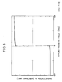
- FIG. 2 shows a magnetoresistance change ⁇ R/R (curve labeled MgO) and
- FIG. 5 shows a magnetization versus applied magnetic field curve.
- a magnetic multilayer [Co(6)-Ag(15)]x70 was fabricated by repeating the procedure of Example 5 except that an amorphous glass substrate was used instead.
- This multilayer also had an axis of easy magnetization within a plane parallel to the surface, a squareness ratio Br/Bs of 0.1, and antiferromagnetism.
- the magnetoresistance change ⁇ R/R was 26.8% in an applied field of 557.2 kA/m (7 kOe) at - 196°C (77K) as measured with a current flow of 125 ⁇ A.
- the magnetoresistance change ⁇ R/R of this multilayer is shown in FIG. 2 as a curve labeled glass.
- a magnetic multilayer [Co(50)-Ag(70)]x30 was fabricated on an amorphous glass substrate.
- the conditions included an ultimate pressure of 160 x 10 -10 Pa (1.2 ⁇ 10 -10 Torr), an operating pressure of 400 x 10- 9 Pa (3.0 ⁇ 10 -9 Torr), and a substrate temperature of 100°C.
- This multilayer showed a magnetization versus applied magnetic field curve as shown in FIG. 6, indicating an in-plane squareness ratio Br/Bs of 0.9 and no antiferromagnetism.
- the magnetoresistance change was only 0.5% at 557.2 (7 kOe) and room temperature.
- Magnetic multilayers [Co(6)-Ag(t)]x70 were fabricated in accordance with Example 1 while the thickness (t) of Ag films was varied.
- the magnetoresistance change rate is defined by the formula:
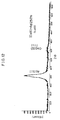
- FIGS. 11 and 12 show X-ray diffraction patterns of the magnetic multilayers on MgO and glass substrates, respectively. It is seen from FIG. 11 that epitaxial growth of (100) orientation took place in the film plane on the MgO substrate. It is seen from FIG. 12 that polycrystalline films formed on the glass substrate.
- Example 1 As in Example 1, 70 units each consisting of a Ni film of 7 ⁇ 10 -10 m(7 ⁇ ) and a Ag film of 10 ⁇ 10 -10 m (10 A) were stacked, fabricating a magnetic multilayer sample designated [Ni (7) -Ag (10) ] x70 having a total thickness of 0.12 ⁇ m. Its magnetization curve and magnetoresistance change at room temperature changed little. This was because the Ni layers as magnetic films had a Curie temperature lower than room temperature as indicated by analysis. When measured at -196°C (77 K), the magnetization curve showed antiferromagnetism as found with Co/Ag, and the magnetoresistance change Ap/ps was 25%.
- a magnetic multilayer designated [Ni(7)-Ag(22)]x70 was fabricated as in Example 8, which showed a Ap/ps of 8% at -196°C (77K).
- a magnetic multilayer designated [Ni(7)-Ag(70)]x70 was fabricated as in Example 8, which showed a Ap/ps of 1% at -196°C (77K).
- a magnetic multilayer capable of giant magnetoresistance change in a lower magnetic field applied as compared with prior art magnetoresistance changing multilayers based on antiferromagnetic coupling.
- a magnetoresistance change of 1 to 40% is available in an operating magnetic field of 0.79 to 1592 kA/m (0.01 to 20 kOe). Since no limit is imposed on the type and temperature of a substrate on which the multilayer is stacked (for example, glass substrates are acceptable), the invention is advantageous for mass scale production. Any desired MR change is obtained by changing the direction of an external magnetic field applied thereto.
Landscapes
- Chemical & Material Sciences (AREA)
- Engineering & Computer Science (AREA)
- Crystallography & Structural Chemistry (AREA)
- Nanotechnology (AREA)
- Physics & Mathematics (AREA)
- Condensed Matter Physics & Semiconductors (AREA)
- General Physics & Mathematics (AREA)
- Power Engineering (AREA)
- Hall/Mr Elements (AREA)
- Thin Magnetic Films (AREA)
Claims (5)
dadurch gekennzeichnet, daß
die Vielschicht eine leichte Magnetisierungsachse in einer Ebene parallel zu der Oberfläche und ein Rechteckverhältnis Br/Bs in der Ebene von bis zu 0,5 aufweist.
dadurch gekennzeichnet, daß
der magnetische Dünnfilm und der Silberdünnfilm durch ein Molekularstrahl-Epitaxieverfahren gebildet sind.
dadurch gekennzeichnet, daß
zumindest ein magnetischer Dünnfilm eine Dicke von 2 bis 60 x 10-10 m (2 bis 60 A) und zumindest ein Silberdünnfilm eine Dicke von 2 bis 60 x 10-10 m (2 bis 60 A) aufweist.
Applications Claiming Priority (6)
| Application Number | Priority Date | Filing Date | Title |
|---|---|---|---|
| JP83290/91 | 1991-03-22 | ||
| JP8329091 | 1991-03-22 | ||
| JP8329091 | 1991-03-22 | ||
| JP18690691 | 1991-07-01 | ||
| JP186906/91 | 1991-07-01 | ||
| JP18690691A JP3320079B2 (ja) | 1991-03-22 | 1991-07-01 | 磁性積層体および磁気抵抗効果素子 |
Publications (3)
| Publication Number | Publication Date |
|---|---|
| EP0504473A1 EP0504473A1 (de) | 1992-09-23 |
| EP0504473B1 true EP0504473B1 (de) | 1995-03-15 |
| EP0504473B2 EP0504473B2 (de) | 2000-03-08 |
Family
ID=26424340
Family Applications (1)
| Application Number | Title | Priority Date | Filing Date |
|---|---|---|---|
| EP91113878A Expired - Lifetime EP0504473B2 (de) | 1991-03-22 | 1991-08-19 | Magnetische Mehrschicht und Element mit Magnetowiderstandseffekt |
Country Status (4)
| Country | Link |
|---|---|
| US (1) | US5366815A (de) |
| EP (1) | EP0504473B2 (de) |
| JP (1) | JP3320079B2 (de) |
| DE (1) | DE69108224T3 (de) |
Families Citing this family (45)
| Publication number | Priority date | Publication date | Assignee | Title |
|---|---|---|---|---|
| EP0506433B2 (de) * | 1991-03-29 | 2007-08-01 | Kabushiki Kaisha Toshiba | Magnetowiderstandseffekt-Element |
| JPH05183212A (ja) * | 1991-07-30 | 1993-07-23 | Toshiba Corp | 磁気抵抗効果素子 |
| JP3346787B2 (ja) | 1991-12-19 | 2002-11-18 | ティーディーケイ株式会社 | 磁性積層体および磁気抵抗効果素子 |
| JP3285937B2 (ja) * | 1992-06-23 | 2002-05-27 | ティーディーケイ株式会社 | 磁性多層膜および磁気抵抗変化素子ならびにそれらの製造方法 |
| JP3411626B2 (ja) * | 1992-08-27 | 2003-06-03 | ティーディーケイ株式会社 | 磁性多層膜および磁気抵抗効果素子ならびにそれらの製造方法 |
| DE69332699T2 (de) * | 1992-11-16 | 2003-09-18 | Nve Corp., Eden Prairie | Magnetoresistive struktur mit einer legierungsschicht |
| US5617071A (en) * | 1992-11-16 | 1997-04-01 | Nonvolatile Electronics, Incorporated | Magnetoresistive structure comprising ferromagnetic thin films and intermediate alloy layer having magnetic concentrator and shielding permeable masses |
| US5569544A (en) * | 1992-11-16 | 1996-10-29 | Nonvolatile Electronics, Incorporated | Magnetoresistive structure comprising ferromagnetic thin films and intermediate layers of less than 30 angstroms formed of alloys having immiscible components |
| US5656381A (en) * | 1993-03-24 | 1997-08-12 | Sanyo Electric Co., Ltd. | Magnetoresistance-effect element |
| US5585198A (en) * | 1993-10-20 | 1996-12-17 | Sanyo Electric Co., Ltd. | Magnetorsistance effect element |
| US5736921A (en) * | 1994-03-23 | 1998-04-07 | Sanyo Electric Co., Ltd. | Magnetoresistive element |
| US5585199A (en) * | 1993-09-09 | 1996-12-17 | Kabushiki Kaisha Toshiba | Magnetoresistance effect head |
| US5422621A (en) * | 1993-10-29 | 1995-06-06 | International Business Machines Corporation | Oriented granular giant magnetoresistance sensor |
| US5695858A (en) * | 1994-03-23 | 1997-12-09 | Sanyo Electric Co., Ltd. | Magnetoresistive element |
| JP2569426B2 (ja) * | 1994-03-24 | 1997-01-08 | 工業技術院長 | 超格子多層膜の製造方法 |
| US5874886A (en) * | 1994-07-06 | 1999-02-23 | Tdk Corporation | Magnetoresistance effect element and magnetoresistance device |
| JPH0849062A (ja) * | 1994-08-04 | 1996-02-20 | Sanyo Electric Co Ltd | 磁気抵抗効果膜 |
| JPH08130337A (ja) * | 1994-09-09 | 1996-05-21 | Sanyo Electric Co Ltd | 磁気抵抗素子及びその製造方法 |
| JP2933841B2 (ja) * | 1994-12-22 | 1999-08-16 | 沖電気工業株式会社 | 情報記録媒体、情報記録・再生方法および情報記録・再生装置 |
| JP3514863B2 (ja) * | 1995-02-01 | 2004-03-31 | 輝也 新庄 | 磁気抵抗効果多層膜、磁気抵抗効果素子および磁気抵抗効果素子の製造方法 |
| US5585986A (en) * | 1995-05-15 | 1996-12-17 | International Business Machines Corporation | Digital magnetoresistive sensor based on the giant magnetoresistance effect |
| US5648885A (en) * | 1995-08-31 | 1997-07-15 | Hitachi, Ltd. | Giant magnetoresistive effect sensor, particularly having a multilayered magnetic thin film layer |
| US5747997A (en) * | 1996-06-05 | 1998-05-05 | Regents Of The University Of Minnesota | Spin-valve magnetoresistance sensor having minimal hysteresis problems |
| US6166539A (en) * | 1996-10-30 | 2000-12-26 | Regents Of The University Of Minnesota | Magnetoresistance sensor having minimal hysteresis problems |
| US5945904A (en) * | 1996-09-06 | 1999-08-31 | Ford Motor Company | Giant magnetoresistors with high sensitivity and reduced hysteresis and thin layers |
| US5976681A (en) * | 1997-06-30 | 1999-11-02 | Ford Global Technologies, Inc. | Giant magnetoresistors with high sensitivity and reduced hysteresis |
| US6340886B1 (en) * | 1997-08-08 | 2002-01-22 | Nonvolatile Electronics, Incorporated | Magnetic field sensor with a plurality of magnetoresistive thin-film layers having an end at a common surface |
| US6404191B2 (en) | 1997-08-08 | 2002-06-11 | Nve Corporation | Read heads in planar monolithic integrated circuit chips |
| JP4303329B2 (ja) | 1998-05-15 | 2009-07-29 | Tdk株式会社 | 磁気抵抗効果膜の製造方法および磁気抵抗効果型ヘッドの製造方法 |
| JP2000331316A (ja) | 1999-05-20 | 2000-11-30 | Tdk Corp | 磁気抵抗効果型ヘッド |
| JP2001006127A (ja) | 1999-06-18 | 2001-01-12 | Tdk Corp | トンネル磁気抵抗効果型ヘッド |
| JP2001006130A (ja) | 1999-06-24 | 2001-01-12 | Tdk Corp | トンネル磁気抵抗効果型ヘッド |
| JP3592140B2 (ja) | 1999-07-02 | 2004-11-24 | Tdk株式会社 | トンネル磁気抵抗効果型ヘッド |
| JP3321768B2 (ja) | 1999-07-23 | 2002-09-09 | ティーディーケイ株式会社 | トンネル磁気抵抗効果素子 |
| JP3400750B2 (ja) | 1999-07-23 | 2003-04-28 | ティーディーケイ株式会社 | トンネル磁気抵抗効果型ヘッドの製造方法 |
| JP3331397B2 (ja) | 1999-07-23 | 2002-10-07 | ティーディーケイ株式会社 | トンネル磁気抵抗効果素子 |
| US6893542B1 (en) | 1999-09-10 | 2005-05-17 | Seagate Technology Llc | Sputtered multilayer magnetic recording media with ultra-high coercivity |
| SE9903481D0 (sv) * | 1999-09-27 | 1999-09-27 | Olle Eriksson | Magnetic field sensor |
| US20060147758A1 (en) * | 2005-01-06 | 2006-07-06 | Hong-Sik Jung | Perpendicular magnetic recording medium with magnetically resetable single domain soft magnetic underlayer |
| US7910159B2 (en) * | 2005-06-03 | 2011-03-22 | Wd Media, Inc. | Radial magnetic field reset system for producing single domain soft magnetic underlayer on perpendicular magnetic recording medium |
| RU2321013C1 (ru) * | 2006-07-25 | 2008-03-27 | Институт проблем технологии микроэлектроники и особочистых материалов Российской Академии Наук (ИПТМ РАН) | Датчик холла для локальной магнитометрии |
| US8063634B2 (en) * | 2008-07-31 | 2011-11-22 | Allegro Microsystems, Inc. | Electronic circuit and method for resetting a magnetoresistance element |
| US9354284B2 (en) | 2014-05-07 | 2016-05-31 | Allegro Microsystems, Llc | Magnetic field sensor configured to measure a magnetic field in a closed loop manner |
| US9322887B1 (en) | 2014-12-01 | 2016-04-26 | Allegro Microsystems, Llc | Magnetic field sensor with magnetoresistance elements and conductive-trace magnetic source |
| JP6597820B2 (ja) * | 2018-03-12 | 2019-10-30 | Tdk株式会社 | 磁気センサおよび位置検出装置 |
Family Cites Families (5)
| Publication number | Priority date | Publication date | Assignee | Title |
|---|---|---|---|---|
| US3350180A (en) * | 1967-10-31 | Magnetic device with alternating lami- na of magnetic material and non-mag- netic metal on a substrate | ||
| US3479156A (en) * | 1966-10-20 | 1969-11-18 | Burton Silverplating Co | Multilayer magnetic coating |
| JPS62264463A (ja) * | 1986-05-12 | 1987-11-17 | Fuji Photo Film Co Ltd | 光磁気記録媒体 |
| US4935311A (en) * | 1987-04-13 | 1990-06-19 | Hitachi, Ltd. | Magnetic multilayered film and magnetic head using the same |
| EP0341521A1 (de) * | 1988-05-09 | 1989-11-15 | Siemens Aktiengesellschaft | Magnetooptisches Speichermedium |
-
1991
- 1991-07-01 JP JP18690691A patent/JP3320079B2/ja not_active Expired - Fee Related
- 1991-08-19 EP EP91113878A patent/EP0504473B2/de not_active Expired - Lifetime
- 1991-08-19 DE DE69108224T patent/DE69108224T3/de not_active Expired - Fee Related
-
1993
- 1993-05-24 US US08/065,443 patent/US5366815A/en not_active Expired - Lifetime
Also Published As
| Publication number | Publication date |
|---|---|
| EP0504473B2 (de) | 2000-03-08 |
| DE69108224D1 (de) | 1995-04-20 |
| JP3320079B2 (ja) | 2002-09-03 |
| EP0504473A1 (de) | 1992-09-23 |
| DE69108224T2 (de) | 1995-09-28 |
| DE69108224T3 (de) | 2001-02-08 |
| US5366815A (en) | 1994-11-22 |
| JPH04363005A (ja) | 1992-12-15 |
Similar Documents
| Publication | Publication Date | Title |
|---|---|---|
| EP0504473B1 (de) | Magnetische Mehrschicht und Element mit Magnetowiderstandseffekt | |
| EP0717422B1 (de) | Film mit Austauschkopplung und magnetoresistives Element | |
| Den Broeder et al. | Magnetic properties and structure of Pd/Co and Pd/Fe multilayers | |
| EP0483373B1 (de) | Magnetwiderstandseffekt-element | |
| US5872502A (en) | Magnetoresistance effect film and production process thereof | |
| US5514452A (en) | Magnetic multilayer film and magnetoresistance element | |
| JP2901501B2 (ja) | 磁性多層膜およびその製造方法ならびに磁気抵抗効果素子 | |
| US5462795A (en) | Magnetoresistance effect element | |
| US5783284A (en) | Magnetic multilayer film, magnetoresistance element, and method for preparing magnetoresistance element | |
| US6004654A (en) | Magnetic multilayer film, magnetoresistance element, and method for preparing magnetoresistance element | |
| US5942309A (en) | Spin valve magnetoresistive device | |
| US5658658A (en) | Magnetoresistance effect elements and method of fabricating the same | |
| US5514469A (en) | Magnetoresistance effect element | |
| US5858455A (en) | Method for forming a lateral giant magnetoresistance multilayer for a magnetoresistive sensor | |
| JP2743806B2 (ja) | 磁気抵抗効果膜およびその製造方法 | |
| US6015632A (en) | Self-assembled giant magnetoresistance lateral multilayer for a magnetoresistive sensor | |
| JP4219021B2 (ja) | 酸化物人工超格子薄膜とその製造方法 | |
| US6001430A (en) | Magnetoresistance effect film and production process thereof | |
| JP2957233B2 (ja) | 磁性多層膜 | |
| JP3346787B2 (ja) | 磁性積層体および磁気抵抗効果素子 | |
| Inomata et al. | Oscillatory interlayer couplings as functions of a ferromagnetic metal layer and a semiconducting spacer in magnetic superlattices | |
| JP3100714B2 (ja) | 磁性積層体および磁気抵抗効果素子 | |
| JPH0567525A (ja) | 磁性積層体およびその製造方法ならびに磁気抵抗効果素子の製造方法 | |
| Kim et al. | Magnetic and structural studies of sputtered Co/Cu multilayer films | |
| JPH0888424A (ja) | 多層膜磁気抵抗効果素子及びその製造方法 |
Legal Events
| Date | Code | Title | Description |
|---|---|---|---|
| PUAI | Public reference made under article 153(3) epc to a published international application that has entered the european phase |
Free format text: ORIGINAL CODE: 0009012 |
|
| AK | Designated contracting states |
Kind code of ref document: A1 Designated state(s): DE FR GB NL |
|
| 17P | Request for examination filed |
Effective date: 19930323 |
|
| 17Q | First examination report despatched |
Effective date: 19930712 |
|
| GRAA | (expected) grant |
Free format text: ORIGINAL CODE: 0009210 |
|
| AK | Designated contracting states |
Kind code of ref document: B1 Designated state(s): DE FR GB NL |
|
| REF | Corresponds to: |
Ref document number: 69108224 Country of ref document: DE Date of ref document: 19950420 |
|
| ET | Fr: translation filed | ||
| PLBI | Opposition filed |
Free format text: ORIGINAL CODE: 0009260 |
|
| PLBF | Reply of patent proprietor to notice(s) of opposition |
Free format text: ORIGINAL CODE: EPIDOS OBSO |
|
| 26 | Opposition filed |
Opponent name: SIEMENS AG Effective date: 19951215 |
|
| NLR1 | Nl: opposition has been filed with the epo |
Opponent name: SIEMENS AG |
|
| PLBF | Reply of patent proprietor to notice(s) of opposition |
Free format text: ORIGINAL CODE: EPIDOS OBSO |
|
| PLBF | Reply of patent proprietor to notice(s) of opposition |
Free format text: ORIGINAL CODE: EPIDOS OBSO |
|
| PLAW | Interlocutory decision in opposition |
Free format text: ORIGINAL CODE: EPIDOS IDOP |
|
| PLAW | Interlocutory decision in opposition |
Free format text: ORIGINAL CODE: EPIDOS IDOP |
|
| PUAH | Patent maintained in amended form |
Free format text: ORIGINAL CODE: 0009272 |
|
| STAA | Information on the status of an ep patent application or granted ep patent |
Free format text: STATUS: PATENT MAINTAINED AS AMENDED |
|
| 27A | Patent maintained in amended form |
Effective date: 20000308 |
|
| AK | Designated contracting states |
Kind code of ref document: B2 Designated state(s): DE FR GB NL |
|
| NLR2 | Nl: decision of opposition | ||
| NLR3 | Nl: receipt of modified translations in the netherlands language after an opposition procedure | ||
| ET3 | Fr: translation filed ** decision concerning opposition | ||
| REG | Reference to a national code |
Ref country code: GB Ref legal event code: IF02 |
|
| PGFP | Annual fee paid to national office [announced via postgrant information from national office to epo] |
Ref country code: FR Payment date: 20020808 Year of fee payment: 12 |
|
| PGFP | Annual fee paid to national office [announced via postgrant information from national office to epo] |
Ref country code: GB Payment date: 20020814 Year of fee payment: 12 |
|
| PGFP | Annual fee paid to national office [announced via postgrant information from national office to epo] |
Ref country code: NL Payment date: 20020829 Year of fee payment: 12 Ref country code: DE Payment date: 20020829 Year of fee payment: 12 |
|
| PG25 | Lapsed in a contracting state [announced via postgrant information from national office to epo] |
Ref country code: GB Free format text: LAPSE BECAUSE OF NON-PAYMENT OF DUE FEES Effective date: 20030819 |
|
| PG25 | Lapsed in a contracting state [announced via postgrant information from national office to epo] |
Ref country code: NL Free format text: LAPSE BECAUSE OF NON-PAYMENT OF DUE FEES Effective date: 20040301 |
|
| PG25 | Lapsed in a contracting state [announced via postgrant information from national office to epo] |
Ref country code: DE Free format text: LAPSE BECAUSE OF NON-PAYMENT OF DUE FEES Effective date: 20040302 |
|
| GBPC | Gb: european patent ceased through non-payment of renewal fee |
Effective date: 20030819 |
|
| PG25 | Lapsed in a contracting state [announced via postgrant information from national office to epo] |
Ref country code: FR Free format text: LAPSE BECAUSE OF NON-PAYMENT OF DUE FEES Effective date: 20040430 |
|
| NLV4 | Nl: lapsed or anulled due to non-payment of the annual fee |
Effective date: 20040301 |
|
| REG | Reference to a national code |
Ref country code: FR Ref legal event code: ST |