EP0507525A1 - Modulateurs pour signaux radio-fréquence - Google Patents
Modulateurs pour signaux radio-fréquence Download PDFInfo
- Publication number
- EP0507525A1 EP0507525A1 EP92302764A EP92302764A EP0507525A1 EP 0507525 A1 EP0507525 A1 EP 0507525A1 EP 92302764 A EP92302764 A EP 92302764A EP 92302764 A EP92302764 A EP 92302764A EP 0507525 A1 EP0507525 A1 EP 0507525A1
- Authority
- EP
- European Patent Office
- Prior art keywords
- mixer
- secam
- signal
- pal
- audio
- Prior art date
- Legal status (The legal status is an assumption and is not a legal conclusion. Google has not performed a legal analysis and makes no representation as to the accuracy of the status listed.)
- Granted
Links
Images


Classifications
-
- H—ELECTRICITY
- H04—ELECTRIC COMMUNICATION TECHNIQUE
- H04N—PICTORIAL COMMUNICATION, e.g. TELEVISION
- H04N5/00—Details of television systems
- H04N5/38—Transmitter circuitry for the transmission of television signals according to analogue transmission standards
- H04N5/40—Modulation circuits
-
- H—ELECTRICITY
- H03—ELECTRONIC CIRCUITRY
- H03C—MODULATION
- H03C5/00—Amplitude modulation and angle modulation produced simultaneously or at will by the same modulating signal
-
- H—ELECTRICITY
- H03—ELECTRONIC CIRCUITRY
- H03D—DEMODULATION OR TRANSFERENCE OF MODULATION FROM ONE CARRIER TO ANOTHER
- H03D7/00—Transference of modulation from one carrier to another, e.g. frequency-changing
- H03D7/14—Balanced arrangements
- H03D7/1408—Balanced arrangements with diodes
-
- H—ELECTRICITY
- H03—ELECTRONIC CIRCUITRY
- H03D—DEMODULATION OR TRANSFERENCE OF MODULATION FROM ONE CARRIER TO ANOTHER
- H03D7/00—Transference of modulation from one carrier to another, e.g. frequency-changing
- H03D7/14—Balanced arrangements
- H03D7/1425—Balanced arrangements with transistors
- H03D7/1433—Balanced arrangements with transistors using bipolar transistors
-
- H—ELECTRICITY
- H03—ELECTRONIC CIRCUITRY
- H03D—DEMODULATION OR TRANSFERENCE OF MODULATION FROM ONE CARRIER TO ANOTHER
- H03D7/00—Transference of modulation from one carrier to another, e.g. frequency-changing
- H03D7/14—Balanced arrangements
- H03D7/1425—Balanced arrangements with transistors
- H03D7/1458—Double balanced arrangements, i.e. where both input signals are differential
-
- H—ELECTRICITY
- H03—ELECTRONIC CIRCUITRY
- H03D—DEMODULATION OR TRANSFERENCE OF MODULATION FROM ONE CARRIER TO ANOTHER
- H03D7/00—Transference of modulation from one carrier to another, e.g. frequency-changing
- H03D7/14—Balanced arrangements
- H03D7/1425—Balanced arrangements with transistors
- H03D7/1475—Subharmonic mixer arrangements
-
- H—ELECTRICITY
- H03—ELECTRONIC CIRCUITRY
- H03D—DEMODULATION OR TRANSFERENCE OF MODULATION FROM ONE CARRIER TO ANOTHER
- H03D2200/00—Indexing scheme relating to details of demodulation or transference of modulation from one carrier to another covered by H03D
- H03D2200/0041—Functional aspects of demodulators
- H03D2200/0088—Reduction of intermodulation, nonlinearities, adjacent channel interference; intercept points of harmonics or intermodulation products
Definitions
- This invention relates to radio frequency modulators.
- PAL television signal is employed in European countries except France
- SECAM television signal is employed in France
- NTSC television signal is employed in Japan and U.S.A.
- a video tape recorder (VTR) for use in France is provided with a radio frequency (RF) modulator using the positive modulation system which is the SECAM modulation system, and a VTR for use in other countries is provided with an RF modulator using the negative modulation system.
- RF radio frequency
- VTRs having RF modulators of a switching type for switching PAL and SECAM television signals for processing are commercially available in those countries.
- FIG. 1 shows a circuit configuration of previously proposed PAL/SECAM switching type RF modulator comprising an integrated circuit (IC) 20 forming a frequency (FM) modulator to which various circuits and switches SW1 to SW3 are connected as external circuit elements.
- IC integrated circuit
- FM frequency
- the switch SW1 switches an audio signal S A applied to an audio input terminal Ain in response to operational modes of the VTR, such as when the VTR is operated in the PAL mode or in the SECAM mode.
- the switch SW1 is externally coupled to the IC 20 for the reason given below.
- the IC 20 is provided with only one FM modulator.
- the FM modulator when operated in the SECAM mode, it is operated as an AM carrier generator. Consequently, when the FM modulator is operated in the SECAM mode, the audio signal S A should be completely prevented from being supplied to the IC 20.
- the switch SW1 is provided to switch the circuits to which the input audio signal is supplied.
- a carrier signal Sc of 6.5 MHz from a terminal (10) of the IC 20 is supplied to an audio amplitude (AM) modulator 22 which then generates a SECAM audio RF signal.
- This audio RF signal is modulated by a video signal which is supplied to the IC 20 through a video signal which is supplied to the IC 20 through a video input terminal Vin, and is thereby added to a video signal from a terminal (12) of the IC 20. Then, the added signal is supplied through an output terminal OUT as an output signal RFout of the RF modulator.
- the switch SW2 is coupled to a terminal (6) of the IC 20.
- the switch SW2 is changed in position to PAL and SECAM contacts, intercarrier generating resonance circuits 24 and 25 respectively connected to terminals (7) and (8) of the IC 20 are switched in response to the PAL mode and the SECAM mode.
- the switch SW3 is provided in order to switch a dc bias of an RF modulator 21 formed of two Schottky diodes 23.
- the radio frequency modulator shown in Figure 1 needs a lot of external assembly parts (about thirteen external parts) each of which is constructed in discrete form. The reason for this is that operation of the FM modulator 21 must be fine adjusted because the PAL and SECAM modes are different in modulation degree, which makes it difficult to build the RF modulator 21 into the IC 20.
- the switch SW2 is indispensable for this RF modulator.
- expensive switches such as a 3-circuit 2-contact switch is needed.
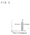
- a video signal S V applied to a video input terminal IN is supplied through a clamping circuit 31 and a white clipping circuit 32 to a mixer circuit 30.
- An audio signal S A applied to an audio input terminal IN is supplied to and amplitude-modulated by an audio AM modulator 33, whereby an output shown in a spectral distribution diagram of Figure 3 is generated from the AM modulator 33. This output signal is supplied to the mixer circuit 30.
- a high frequency signal is supplied from an RF carrier generating source 34 to the mixer circuit 30, in which it is mixed with the video signal S V and the audio signal S A , whereby a high frequency signal RF having the same format as that of the television signal is generated.
- This high frequency signal RF is supplied through an amplifier 35 to an output terminal OUT.
- the RF modulator Since the RF output is generated as described above, the RF modulator has the disadvantage that intermodulation distortions occur in the video signal S V and in the audio signal S A .
- Figure 4 is a diagram showing an example of a circuit configuration of a previously proposed RF modulator fabricated as an IC.
- Figure 5 is a diagram used to explain operation of a main portion of the circuit of Figure 4.
- a double balance mixer circuit 30 comprises a differential circuit formed of transistors Q1, Q2, and a differential circuit formed of transistors Q3, Q4.
- the audio signal S A is supplied to a differential circuit formed of transistors Q11, Q12, and the video signal S A is supplied to a differential circuit formed of the transistors Q13, Q14.
- An output of a local oscillator OSC is supplied to the bases of transistors QA, QB forming a mixer driver, and is also supplied to the bases of transistors Q1 to Q4 forming the double balance mixer circuit 30.
- a reference letter A in Figure 6 is employed as an index by which the sound beat caused by the intermodulation distortion component is detected, and is expressed by a relative ratio of the maximum value of the carrier relative to the interference component. Since the intermodulation distortion is increased and the above-mentioned ratio A is reduced, the sound beat on the picture screen becomes conspicuous. Therefore, A is preferably 65 dB or more.
- an RF modulator comprising: a double balance type mixer for generating an RF output signal by modulating a high frequency signal supplied thereto from an RF carrier generating source with a predetermined signal; a switching circuit for switching a flow current of said double balance type mixer in response to the PAL mode and the SECAM mode; a SECAM audio modulator for amplitude-modulating a SECAM audio signal supplied thereto and supplying an amplitude-modulated SECAM audio signal to said double balance type mixer; a PAL audio modulator for frequency-modulating a PAL audio signal supplied thereto and supplying a frequency-modulated PAL audio signal to said mixer; and a PAL/SECAM switching circuit for controlling operational states of respective circuits in response to a mode switching signal supplied thereto, so that an audio signal is amplitude-modulated and a video signal is positively modulated in the SECAM mode, while the audio signal is frequency-modulated and the video signal is negatively modulated in the PAL mode.
- a RF modulator comprising: a double balance type mixer for generating an RF output signal by modulating a high frequency signal supplied thereto from an RF carrier generating source with a predetermined signal; a switching circuit for switching a flow current of said mixer in response to the PAL mode and the SECAM mode; a SECAM audio modulator for amplitude-modulating a SECAM audio signal supplied thereto and supplying an amplitude-modulated SECAM audio signal to said mixer; a PAL audio modulator for frequency-modulating a PAL audio signal supplied thereto and supplying a frequency-modulated PAL audio signal to said mixer; and a voltage generating circuit for generating a voltage of magnitude corresponding to a flow of current in said mixer thereby automatically to compensate for a deviation of the RF level caused by different modulation degrees in the PAL and SECAM modes; and a PAL/SECAM switching circuit for controlling operational states of respective circuits in response to a mode switching signal supplied thereto, so that an audio signal is
- a RF modulator comprising: an audio mixer circuit supplied with an audio signal; a video mixer circuit supplied with a video signal; a first mixer driver for driving said audio mixer circuit; a second mixer driver for driving said video mixer circuit, said first and second mixer circuits being driven independently; an adding circuit for adding an output of said audio mixer circuit and an output of said video mixer circuit to generate an RF output signal.
- An embodiment of the present invention can provide an RF modulator which can be made compact in size, and is free from adjustment.
- Such a modulator can have an improved intermodulation distortion characteristic, and prevent a sound beat from being produced on a picture screen due to an intermodulation distortion.
- the RF modulator includes a SECAM mixer circuit 52 and a PAL mixer circuit 53, and a SECAM audio signal S SECAM and a PAL audio signal S PAL applied to terminals T 3 , T 4 are respective supplied through an AM modulator 50 and an FM modulator 51 to the mixer circuits 52 and 53.
- a first mixer driver 54 drives the SECAM mixer circuit 52, and a second mixer driver 55 drives the PAL mixer circuit 53, the mixer circuits 52, 53 being independently driven by the mixer drivers 54, 55.
- Carrier high frequency outputs are respectively supplied to the mixer drivers 54, 55 from an OSC buffer amplifier 56. That is, an RF carrier applied to a terminal T1 is supplied to the buffer amplifier 56, in which it is separated into carriers of two systems and then supplied to the first and second mixer driver 54, 55, respectively.
- a video signal S V supplied through a terminal T5 to the IC 40 is supplied through a video clamping circuit 62 to the PAL mixer circuit 53.
- a mode switching signal S M supplied to the terminal T6 is supplied to a change-over switch 63 that is used to switch the PAL and SECAM modes.
- the mode change-over switch 63 responds to the mode switching signal S M supplied thereto to control operation of the AM modulator 50 and the FM modulator 51, and also to control operation of the PAL mixer circuit 53. Since the modulation degree of a video signal is different in the PAL mode and in the SECAM mode, operation of a video modulation degree fine adjusting circuit 64 is controlled so as to avoid the disadvantages which may occur when the operational mode is switched.
- the adjusting circuit 64 is coupled through a terminal T7 to a variable resistor 66, and the video modulation degree can be controlled with high accuracy by adjusting the variable resistor 66.
- the AM modulator 50 and the FM modulator 51 are provided independently, and are provided with respective independent oscillators.
- the operational characteristics of the modulators 50, 51 need not be fine adjusted.
- all circuit elements of the modulators 50, 51 can be fabricated in the IC 40, so that the operation of the PAL and SECAM systems can be switched by a simple change-over switch fabricated in the IC 40. Therefore, an expensive switch need not be coupled to the IC 40 externally.
- Figure 8 is a diagram showing a circuit configuration of the RF modulator of Figure 7 in the form of an IC. Specific arrangements of the respective circuits will be described below with reference to the circuit configuration of Figure 8 in which only the circuits of the PAL signal system are illustrated in the form of a discrete circuit. The circuits of the SECAM signal system are constructed similarly.
- the SECAM mixer circuit 52 and the PAL mixer circuit 53 are each formed as a double balance type mixer.
- a switching circuit 67 is provided in order to switch the flow of an output current of the double balance type mixer 53, and a voltage generating circuit 68, formed of resistors RL1, RL2 connected in series, is provided to generate a voltage of a value corresponding to the flow of the output current of the double balance type mixer circuit 53.
- This voltage generating circuit 68 corrects an RF output level by adjusting the value of the voltage generated by the circuit 68 in response to the PAL system and the SECAM system, whereby an output of substantially the same level is obtained regardless of the PAL system/SECAM system.
- the switching circuit 63 for switching operation of the audio AM/audio FM modulators 50, 51 is formed of two differential circuits as shown in Figure 8, and the modulators 50 and 51 are selectively operated by the output of one of the differential circuits, thereby to carry out the mode switching operation.
- mode switching is carried out, in which, as shown in an operation waveform diagram of Figure 9, the modulation polarity of an input video signal is switched to a positive modulation or to a negative modulation. Then, only when the RF modulator is operated in the SECAM mode, a current source 65 for fine adjusting a mixer current is operated so as to adjust the positive modulation degree.
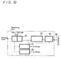
- Figure 10 is a schematic block diagram showing an arrangement of the PAL/SECAM switching system in the above embodiment. As shown, operational states of the audio modulators 50, 51, the video modulator 53, the SECAM fine adjusting circuit 64, the RF level switching circuit 67 and the like can be switched by a DC switch of a simple arrangement which can be fabricated into the IC 40, to simplify the otherwise very complex circuit arrangement.
- the SECAM audio signal S SECAM and the PAL audio signal S PAL are mixed by the adding amplifier 57 and supplied through the output terminal T2 as the RF output signal RFout.
- the RF processing circuits of two systems are provided, and the RF-processed signals are mixed by the adding amplifier 57, thereby to generate the RF modulator output RFout, the occurrence of the intermodulation distortion can be avoided.
- the occurrence of sound beat in which shift of the audio signal appears as a modulation component even in the complete absence of the video signal.
- the mixer circuits for generating the RF output signal are formed as double-balance type mixer circuits, and the voltage generating circuit generates the voltage whose value corresponds to the flow of current in the double-balance type mixer circuits, a deviation of the RF level due to different modulation degrees of the PAL and SECAM modes can be automatically compensated for. Accordingly, the adjustment for switching the operation of the PAL and SECAM modes is not needed, and the external adjusting circuit parts coupled to the IC are not needed. Further, since the required characteristics of the mixer circuits are eased, the adjustment of the AM and FM audio modulators can be made unnecessary, whereby the whole of the audio modulators can be fabricated in the IC. Therefore, the RF modulator can be wholly fabricated as the IC and the RF modulator can be formed without the expensive switch. Thus, the RF modulator can be made compact and inexpensive.
- the RF modulator of this embodiment includes an audio mixer circuit 72 and a video mixer circuit 76, and the audio signal S A and the video signal S U are respectively supplied to the mixer circuits 72 and 76.
- a first mixer driver 73 is provided to drive the audio mixer circuit 72, and a second mixer driver 75 is similarly provided in order to drive the video mixer circuit 76.
- the first and second mixer drivers 73 and 75 are driven independently.
- a high frequency carrier from a buffer amplifier 74 that is, an oscillation output of a local oscillator OSC, is supplied from the outside to the mixer drivers 73 and 75, in which it is separated into signals of two systems. These signals of two systems are respectively supplied to the first and second mixer drivers 73 and 75.
- the audio signal S A and video signal S U respectively modulated by the audio mixer circuit 72 and the video mixer circuit 76 are added by an addition amplifier 71, and supplied from an output terminal Out as an RF output signal.
- the audio mixer circuit 72 performs the balance operation, whereby the carrier is suppressed.
- Figure 12 is a schematic diagram showing a circuit configuration which can form the RF modulator shown in Figure 11.
- the video mixer circuit 76 to which the video signal S U is supplied comprises a differential circuit formed of transistors Q21, Q22, and a differential circuit formed of transistors Q23, Q24. Also, the second mixer driver 75 is arranged such that transistors Q25, Q26 are respectively connected to the collectors of transistors forming a differential circuit.
- the audio mixer circuit 72 to which the audio signal S A is supplied comprises a differential circuit formed of transistors Q27, Q28, and a differential circuit formed of transistors Q29, Q30. Also, the first mixer driver 73 is arranged such that transistors Q31, Q32 are respectively coupled to the collectors of transistors forming a differential circuit.
- Outputs of the audio mixer circuit 72 and the video mixer circuit 76 are supplied through emitter-follower circuits to the addition amplifier 71, and then fed to the bases of differential transistors forming the addition amplifier 71. Then, a signal, which results from adding the output of the audio mixer circuit 72 and the output of the video mixer circuit 76, is developed at the collector of the differential transistor and then fed to the output terminal Out.
- this RF modulator Since this RF modulator generates the RF signal output as described above, a sound beat interference occurring on the picture screen due to intermodulation distortion component can be reliably avoided. Thus, it is possible to form the SECAM modulator which can obtain an intermodulation distortion ratio of about 70 dB or more. Further, since the intermodulation distortion characteristic is improved as described above, the high frequency balance adjustment, which was previously carried out to improve the intermodulation distortion characteristic, can be made unnecessary, so the RF modulator is free from the adjustment. As a consequence, the modulator can be fabricated as the IC and the RF modulator can be miniaturized.
- the two mixer drivers are provided respectively to drive the audio mixer circuit and the video mixer circuit and the RF output signal is obtained by adding two high frequency signals after the RF modulation has ended, the occurrence of intermodulation distortion can be avoided, and the intermodulation distortion characteristic can be improved. Accordingly, the occurrence of sound beat interference on the picture screen due to the intermodulation distortion component can be avoided, which makes the high frequency balance adjustment for improving the intermodulation distortion characteristic unnecessary.
- the modulator can be fabricated as an IC and a miniaturized RF modulator realized.
Landscapes
- Engineering & Computer Science (AREA)
- Power Engineering (AREA)
- Multimedia (AREA)
- Signal Processing (AREA)
- Amplitude Modulation (AREA)
Applications Claiming Priority (4)
| Application Number | Priority Date | Filing Date | Title |
|---|---|---|---|
| JP99460/91 | 1991-04-03 | ||
| JP09946091A JP3169388B2 (ja) | 1991-04-03 | 1991-04-03 | Rfモジュレータ |
| JP09945991A JP3222484B2 (ja) | 1991-04-03 | 1991-04-03 | Rfモジュレータ |
| JP99459/91 | 1991-04-03 |
Publications (2)
| Publication Number | Publication Date |
|---|---|
| EP0507525A1 true EP0507525A1 (fr) | 1992-10-07 |
| EP0507525B1 EP0507525B1 (fr) | 1997-06-11 |
Family
ID=26440594
Family Applications (1)
| Application Number | Title | Priority Date | Filing Date |
|---|---|---|---|
| EP92302764A Expired - Lifetime EP0507525B1 (fr) | 1991-04-03 | 1992-03-30 | Modulateurs pour signaux radio-fréquence |
Country Status (4)
| Country | Link |
|---|---|
| EP (1) | EP0507525B1 (fr) |
| KR (1) | KR100262790B1 (fr) |
| DE (1) | DE69220276T2 (fr) |
| MY (1) | MY110438A (fr) |
Cited By (2)
| Publication number | Priority date | Publication date | Assignee | Title |
|---|---|---|---|---|
| WO1995000859A1 (fr) * | 1993-06-17 | 1995-01-05 | The Canadian Space Agency, An Agency Of The Government Of Canada | Systeme et procede de modulation d'une frequence porteuse |
| WO1997026710A1 (fr) | 1996-01-19 | 1997-07-24 | Motorola Inc. | Procede et dispositif pour effectuer une selection parmi une pluralite de melangeurs |
Citations (2)
| Publication number | Priority date | Publication date | Assignee | Title |
|---|---|---|---|---|
| EP0107295A2 (fr) * | 1982-08-30 | 1984-05-02 | Pioneer Electronic Corporation | Système d'enregistrement et de reproduction du type vidéodisque |
| EP0154318A1 (fr) * | 1984-03-05 | 1985-09-11 | Alps Electric Co., Ltd. | Circuit de modulation à haute fréquence |
-
1992
- 1992-03-30 EP EP92302764A patent/EP0507525B1/fr not_active Expired - Lifetime
- 1992-03-30 DE DE69220276T patent/DE69220276T2/de not_active Expired - Fee Related
- 1992-04-01 MY MYPI92000560A patent/MY110438A/en unknown
- 1992-04-02 KR KR1019920005493A patent/KR100262790B1/ko not_active Expired - Fee Related
Patent Citations (2)
| Publication number | Priority date | Publication date | Assignee | Title |
|---|---|---|---|---|
| EP0107295A2 (fr) * | 1982-08-30 | 1984-05-02 | Pioneer Electronic Corporation | Système d'enregistrement et de reproduction du type vidéodisque |
| EP0154318A1 (fr) * | 1984-03-05 | 1985-09-11 | Alps Electric Co., Ltd. | Circuit de modulation à haute fréquence |
Non-Patent Citations (1)
| Title |
|---|
| PATENT ABSTRACTS OF JAPAN vol. 7, no. 200 (E-196)3 September 1983 & JP-A-58 097 975 ( MATSUSHITA DENKI SANGYO KK ) 10 June 1983 * |
Cited By (3)
| Publication number | Priority date | Publication date | Assignee | Title |
|---|---|---|---|---|
| WO1995000859A1 (fr) * | 1993-06-17 | 1995-01-05 | The Canadian Space Agency, An Agency Of The Government Of Canada | Systeme et procede de modulation d'une frequence porteuse |
| WO1997026710A1 (fr) | 1996-01-19 | 1997-07-24 | Motorola Inc. | Procede et dispositif pour effectuer une selection parmi une pluralite de melangeurs |
| EP0875094A4 (fr) * | 1996-01-19 | 2004-05-19 | Motorola Inc | Procede et dispositif pour effectuer une selection parmi une pluralite de melangeurs |
Also Published As
| Publication number | Publication date |
|---|---|
| DE69220276D1 (de) | 1997-07-17 |
| MY110438A (en) | 1998-05-30 |
| KR100262790B1 (ko) | 2000-08-01 |
| EP0507525B1 (fr) | 1997-06-11 |
| KR920020939A (ko) | 1992-11-21 |
| DE69220276T2 (de) | 1997-11-13 |
Similar Documents
| Publication | Publication Date | Title |
|---|---|---|
| CA1051529A (fr) | Circuit modulateur haute frequence | |
| US4747159A (en) | RF modulator | |
| US4223342A (en) | Circuit for improving the frequency characteristic of a color television signal | |
| US3961361A (en) | Gain control arrangement useful in a television signal processing system | |
| KR100202345B1 (ko) | 텔레비젼온-스크린 문자 디스플레이 시스템 | |
| US3946152A (en) | Correction system for video signals having a limited amplitude range | |
| EP0507525B1 (fr) | Modulateurs pour signaux radio-fréquence | |
| EP0189931B1 (fr) | modulateur d'amplitude | |
| US3780219A (en) | Signal processing circuit | |
| US4933972A (en) | Stereo multiplex demodulator | |
| US4343018A (en) | Chrominance signal processing circuit | |
| US4038681A (en) | Chroma-burst separator and amplifier | |
| JP3222484B2 (ja) | Rfモジュレータ | |
| US4349834A (en) | Chroma signal gain control circuit | |
| US4449230A (en) | Apparatus for demodulating an AM stereophonic signal | |
| US4370680A (en) | Color signal processing device for video recorder | |
| EP0521472B1 (fr) | Dispositif de traitement de signal d'image | |
| US3833823A (en) | Signal processing circuit for a color television receiver | |
| US5706350A (en) | Stereophonic decoder | |
| JP3169388B2 (ja) | Rfモジュレータ | |
| KR940008100Y1 (ko) | 채널의 혼신방지가 가능한 무선주파수변조장치 | |
| US3701844A (en) | Color compensating network for an integrated circuit television receiver | |
| US4764810A (en) | Horizontal phase locked loop system | |
| EP0510571B1 (fr) | Circuit de traitement de signal de couleur pour un enregistreur à cassettes vidéo | |
| CA1227547A (fr) | Demodulateur mf |
Legal Events
| Date | Code | Title | Description |
|---|---|---|---|
| PUAI | Public reference made under article 153(3) epc to a published international application that has entered the european phase |
Free format text: ORIGINAL CODE: 0009012 |
|
| AK | Designated contracting states |
Kind code of ref document: A1 Designated state(s): DE FR GB NL |
|
| 17P | Request for examination filed |
Effective date: 19930224 |
|
| 17Q | First examination report despatched |
Effective date: 19950504 |
|
| GRAG | Despatch of communication of intention to grant |
Free format text: ORIGINAL CODE: EPIDOS AGRA |
|
| GRAH | Despatch of communication of intention to grant a patent |
Free format text: ORIGINAL CODE: EPIDOS IGRA |
|
| GRAH | Despatch of communication of intention to grant a patent |
Free format text: ORIGINAL CODE: EPIDOS IGRA |
|
| GRAA | (expected) grant |
Free format text: ORIGINAL CODE: 0009210 |
|
| AK | Designated contracting states |
Kind code of ref document: B1 Designated state(s): DE FR GB NL |
|
| REF | Corresponds to: |
Ref document number: 69220276 Country of ref document: DE Date of ref document: 19970717 |
|
| ET | Fr: translation filed | ||
| PLBE | No opposition filed within time limit |
Free format text: ORIGINAL CODE: 0009261 |
|
| STAA | Information on the status of an ep patent application or granted ep patent |
Free format text: STATUS: NO OPPOSITION FILED WITHIN TIME LIMIT |
|
| 26N | No opposition filed | ||
| REG | Reference to a national code |
Ref country code: GB Ref legal event code: IF02 |
|
| PGFP | Annual fee paid to national office [announced via postgrant information from national office to epo] |
Ref country code: NL Payment date: 20050303 Year of fee payment: 14 |
|
| PGFP | Annual fee paid to national office [announced via postgrant information from national office to epo] |
Ref country code: FR Payment date: 20050308 Year of fee payment: 14 |
|
| PGFP | Annual fee paid to national office [announced via postgrant information from national office to epo] |
Ref country code: DE Payment date: 20050324 Year of fee payment: 14 |
|
| PGFP | Annual fee paid to national office [announced via postgrant information from national office to epo] |
Ref country code: GB Payment date: 20050330 Year of fee payment: 14 |
|
| PG25 | Lapsed in a contracting state [announced via postgrant information from national office to epo] |
Ref country code: GB Free format text: LAPSE BECAUSE OF NON-PAYMENT OF DUE FEES Effective date: 20060330 |
|
| PG25 | Lapsed in a contracting state [announced via postgrant information from national office to epo] |
Ref country code: NL Free format text: LAPSE BECAUSE OF NON-PAYMENT OF DUE FEES Effective date: 20061001 |
|
| PG25 | Lapsed in a contracting state [announced via postgrant information from national office to epo] |
Ref country code: DE Free format text: LAPSE BECAUSE OF NON-PAYMENT OF DUE FEES Effective date: 20061003 |
|
| GBPC | Gb: european patent ceased through non-payment of renewal fee |
Effective date: 20060330 |
|
| NLV4 | Nl: lapsed or anulled due to non-payment of the annual fee |
Effective date: 20061001 |
|
| REG | Reference to a national code |
Ref country code: FR Ref legal event code: ST Effective date: 20061130 |
|
| PG25 | Lapsed in a contracting state [announced via postgrant information from national office to epo] |
Ref country code: FR Free format text: LAPSE BECAUSE OF NON-PAYMENT OF DUE FEES Effective date: 20060331 |