EP0512685A1 - Quadraturbusprotokoll zum Ausführen von Transaktionen in einer Rechneranordnung - Google Patents
Quadraturbusprotokoll zum Ausführen von Transaktionen in einer Rechneranordnung Download PDFInfo
- Publication number
- EP0512685A1 EP0512685A1 EP92303034A EP92303034A EP0512685A1 EP 0512685 A1 EP0512685 A1 EP 0512685A1 EP 92303034 A EP92303034 A EP 92303034A EP 92303034 A EP92303034 A EP 92303034A EP 0512685 A1 EP0512685 A1 EP 0512685A1
- Authority
- EP
- European Patent Office
- Prior art keywords
- bus
- computer system
- processors
- state
- address
- Prior art date
- Legal status (The legal status is an assumption and is not a legal conclusion. Google has not performed a legal analysis and makes no representation as to the accuracy of the status listed.)
- Granted
Links
Images


Classifications
-
- G—PHYSICS
- G06—COMPUTING OR CALCULATING; COUNTING
- G06F—ELECTRIC DIGITAL DATA PROCESSING
- G06F9/00—Arrangements for program control, e.g. control units
- G06F9/06—Arrangements for program control, e.g. control units using stored programs, i.e. using an internal store of processing equipment to receive or retain programs
- G06F9/30—Arrangements for executing machine instructions, e.g. instruction decode
- G06F9/38—Concurrent instruction execution, e.g. pipeline or look ahead
-
- G—PHYSICS
- G06—COMPUTING OR CALCULATING; COUNTING
- G06F—ELECTRIC DIGITAL DATA PROCESSING
- G06F15/00—Digital computers in general; Data processing equipment in general
- G06F15/16—Combinations of two or more digital computers each having at least an arithmetic unit, a program unit and a register, e.g. for a simultaneous processing of several programs
- G06F15/163—Interprocessor communication
- G06F15/17—Interprocessor communication using an input/output type connection, e.g. channel, I/O port
-
- G—PHYSICS
- G06—COMPUTING OR CALCULATING; COUNTING
- G06F—ELECTRIC DIGITAL DATA PROCESSING
- G06F12/00—Accessing, addressing or allocating within memory systems or architectures
- G06F12/02—Addressing or allocation; Relocation
- G06F12/08—Addressing or allocation; Relocation in hierarchically structured memory systems, e.g. virtual memory systems
- G06F12/0802—Addressing of a memory level in which the access to the desired data or data block requires associative addressing means, e.g. caches
- G06F12/0806—Multiuser, multiprocessor or multiprocessing cache systems
- G06F12/0815—Cache consistency protocols
- G06F12/0831—Cache consistency protocols using a bus scheme, e.g. with bus monitoring or watching means
-
- G—PHYSICS
- G06—COMPUTING OR CALCULATING; COUNTING
- G06F—ELECTRIC DIGITAL DATA PROCESSING
- G06F13/00—Interconnection of, or transfer of information or other signals between, memories, input/output devices or central processing units
- G06F13/14—Handling requests for interconnection or transfer
- G06F13/36—Handling requests for interconnection or transfer for access to common bus or bus system
- G06F13/368—Handling requests for interconnection or transfer for access to common bus or bus system with decentralised access control
Definitions
- the present invention relates generally to pipelined-bus protocols for carrying out transactions in a computer system. More particularly, the invention relates to a method and corresponding apparatus for carrying out transactions in a multi-processor computer system by dividing the transactions into "quadrature state" processes.
- Many computer systems include a plurality of processing units, e.g., master processors, that simultaneously interact with shared resources, such as I/O devices, slave processors and memory devices.
- the master processors of these systems are typically coupled to the various resources via a single address bus and a single data bus. Signals to/from the respective master processors must be sent from/to the respective resource devices over one of these buses.
- bandwidth There are three important parameters that must be considered when defining a bus: bandwidth, latency and cost.
- Bandwidth is a measure of the quantity of data that can be transferred over the bus per second. Bandwidth is important because the data bus connecting the memory devices to the master processors can create a "bottleneck" through which all memory transactions must pass; thus, a large-bandwidth data bus is important to the overall speed of the computer system.
- Latency represents the time it takes to transfer data between memory and a processor.
- a great deal of complexity can be added to a system to improve bandwidth and latency; however, this added complexity increases the cost of the system.
- a goal of the bus designer is to maximize bandwidth and minimize latency for the least possible cost.
- a protocol is required for accessing the address bus when more than one of the master processors "desires" to conduct a transaction with one of the resources, e.g., a read or write to or from memory.
- the protocol facilitate a simplified bus design by standardizing all transactions. It is further desirable that the protocol not require the memory devices to be complex, or "smart.” The present invention achieves these goals.
- the invention provides a method for carrying out transactions between a processor and a slave or memory device, such as, e.g., a slave processor.
- a method comprises the steps of first identifying one of the processors as having priority over the other processors to access of the bus, this step is performed during a first state of the computer system.
- data is transferred between one of the slave devices and the identified one of the processors.
- a slave device address is transferred from the processor having priority (i.e., priority to access of the bus) to the bus.
- a virtual address is transferred from the processor having won priority to the slave device via the bus.
- the invention also provides a computer system comprising a plurality of master processors, at least one slave or memory device, a bus coupling the master processors to the slave or memory device, and means for implementing a protocol for carrying out a transaction between one of the master processors and the slave or memory device.
- the means for carrying out the protocol comprises means for carrying out the above method steps.
- An alternative computer system in accordance with the invention includes a plurality of processors and memory devices interconnected via a bus, with all transactions between the processors and memory devices carried out in accordance with the following protocol: First, a plurality of periodic states during which the transactions are to be conducted is defined. The states should each have a fixed duration in time and recur between fixed intervals. Next, each transaction is divided into a prescribed number of processes, each process to be carried out during a predefined one of the periodic states. This protocol makes the processors capable of determining whether a given memory device is busy before attempting to carry out a transaction with the given device.
- FIG. 1 is a block diagram of a pipelined multi-processor computer system in accordance with the present invention.
- Figure 2 is a flowchart of a method of carrying out transactions in a pipelined multi-processor computer system in accordance with the present invention.
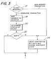
- Figure 3 is a flowchart of a method of arbitrating access to a bus, corresponding to block 10 of Figure 2.
- Figure 4 is an expanded view of the slave address block 14 of Figure 2.
- Figure 5 is an expanded view of the virtual address block 16 of Figure 2.
- FIGS. 6A-6F together make up a timing diagram for a computer system in accordance with the present invention.
- the present invention is an attempt to maximize bandwidth and latency in a computer system while keeping complexity and cost at a reasonable level. It accomplishes this by combining pipelining with a novel address bus protocol.
- the address bus is split into groups of 4 states, known as "quads.” Control of the bus is simplified by defining all transactions to consist of these 4 states.
- the 4 states are the "arbitrate state”, "I/O state”, "slave address state”, and "virtual address state.” Because the bus is pipelined and all transactions take the same amount of time, the invention allows a processor to determine beforehand whether the memory block it needs to access is busy with a request from another processor; thus it can inhibit its arbitration until it determines the memory block is free. This reduces the number of transactions on the bus that must be "busied” (retried) by the processor, which improves bandwidth.
- Figure 1 depicts a pipelined computer system in accordance with the present invention.
- the system of Figure 1 comprises a plurality of master processors ("MPs") 2a, 2b, 2c, etc., each of which is coupled to an associated unit of high speed cache memory 6a, 6b, 6c, etc.
- the master processors 2a, 2b, 2c, etc. are also coupled via an address bus to one or more slave processors 4a, 4b (e.g., a slave I/O unit and a slave processor) and a unit of main memory 5.
- the high speed cache units 6a, 6b, 6c, etc. are loaded with data or instructions, at medium speed, from main memory 5 via data bus 9.
- All transactions between master processors 2a, 2b, 2c, etc., and slave processors 4a, 4b or main memory 5 are divided into an address quad and an associated data quad.
- the data quad is performed during a fixed interval of time following its associated address quad.
- the standardization of all transactions simplifies the design of interfaces between the various components of the system.
- the standardization also simplifies memory design, since memory simply starts its address bus accesses during an address quad and dumps data during a corresponding data quad.
- an address quad in accordance with the invention comprises four states of fixed duration during which various processes are carried out, the processes directed toward executing a transaction between a master processor and slave I/O device 4a, slave processor 4b or memory device 5.
- the address quad comprises an arbitrate state 10, an I/O state 12, a slave address (SA) state 14 and a virtual address (VA) state 16.
- SA slave address
- VA virtual address
- the various master processors 2a, 2b, 2c, etc. contend for access to the address bus 8. This procedure is described more fully below with reference to Figure 3.
- the address of the slave device 4a, 4b to be transacted with by the winning master processor 2a, 2b, 2c, etc. is transmitted onto address bus 8, from which it can be received by the respective slave devices.
- three parallel operations 14a, 14b, 14c take place: the slave address is sent onto the address bus, block 14a, a transaction type (TT) identifier is sent onto the address bus, block 14b, and a block ID (BLK ID) number is sent onto the address bus, block 14c. These operations are preferably performed simultaneously. Note that the block ID number is employed for interleaving blocks of memory.
- a virtual address is transmitted from the master processor having won priority over the address bus (during the arbitrate state 10) to the address bus.
- the virtual address state 16 is used for cache coherency checking, i.e., checking to ensure that all of the cache memory units 6a, 6b, 6c, etc., contain identical data for the same address.
- the master processor address (MA) i.e., the address of the master processor with priority over the address bus
- MA master processor address
- the master processor determines the status of the intended device. If a non-memory device is busy, it sends a busy status signal (ST (see Figures 6D-6F)) to the master processor. Thus, if the device to be accessed is an I/O device 4a or slave processor 4b, no mapping or status check is required; the master processor is free to arbitrate provided the I/O device is not busy.
- the master checks the status of a memory device by maintaining a list of memory block ID numbers sent onto the bus during the previous N states. Typically, N corresponds to the number of states within the previous 120 ns. If the memory device hasn't been accessed during the previous N states it is assumed to be not busy, and the master processor is free to arbitrate.
- step 24 a determination is made of which master processor is to be given priority to the bus, step 24.
- the determination of priority may be made on any one of a number of known arbitration algorithms, e.g., an LRU (least recently used) or DPL (distributed priority list) algorithm.
- FIG. 6A-6F The relationship between the address quads 10, 12, 14, 16 and data quads D0, D1, D2, D3 is shown in Figures 6A-6F. Five address quads are shown. The first two are memory transactions in which data is returned on the data bus some fixed time after the corresponding address quad. Typical times are 120ns after the corresponding slave address state.
- memory accesses are usually in lines, but may also be in double lines, half lines, bytes, etc.
- a line is simply a standard number of bytes associated with a particular cache "tag".
- the processor attempts to read a memory location in cache, and misses, it will issue a memory transaction over the bus.
- a line (e.g., 32 bytes) will be loaded into cache and associated with a particular cache tag. If the transaction is with an I/O register, the data is returned via address bus 8 during the I/O state of the address quad. This is done to allow inexpensive I/O device implementations that don't have to be connected to data bus 9.
Landscapes
- Engineering & Computer Science (AREA)
- Theoretical Computer Science (AREA)
- Physics & Mathematics (AREA)
- General Engineering & Computer Science (AREA)
- General Physics & Mathematics (AREA)
- Computer Hardware Design (AREA)
- Software Systems (AREA)
- Memory System Of A Hierarchy Structure (AREA)
- Multi Processors (AREA)
- Bus Control (AREA)
Applications Claiming Priority (2)
| Application Number | Priority Date | Filing Date | Title |
|---|---|---|---|
| US694265 | 1991-04-29 | ||
| US07/694,265 US5249297A (en) | 1991-04-29 | 1991-04-29 | Methods and apparatus for carrying out transactions in a computer system |
Publications (2)
| Publication Number | Publication Date |
|---|---|
| EP0512685A1 true EP0512685A1 (de) | 1992-11-11 |
| EP0512685B1 EP0512685B1 (de) | 1999-12-29 |
Family
ID=24788104
Family Applications (1)
| Application Number | Title | Priority Date | Filing Date |
|---|---|---|---|
| EP92303034A Expired - Lifetime EP0512685B1 (de) | 1991-04-29 | 1992-04-06 | Quadraturbusprotokoll zum Ausführen von Transaktionen in einer Rechneranordnung |
Country Status (5)
| Country | Link |
|---|---|
| US (1) | US5249297A (de) |
| EP (1) | EP0512685B1 (de) |
| JP (1) | JPH05274252A (de) |
| KR (1) | KR920020316A (de) |
| DE (1) | DE69230483T2 (de) |
Families Citing this family (16)
| Publication number | Priority date | Publication date | Assignee | Title |
|---|---|---|---|---|
| WO1994010632A1 (de) * | 1992-11-04 | 1994-05-11 | Siemens Aktiengesellschaft | Anordnung mit mehreren aktiven und passiven busteilnehmern |
| JP2826028B2 (ja) * | 1993-01-28 | 1998-11-18 | 富士通株式会社 | 分散メモリ型プロセッサシステム |
| CA2116826C (en) * | 1993-03-11 | 1998-11-24 | Timothy J. Sullivan | Data processing system using a non-multiplexed, asynchronous address/data bus system |
| US5581713A (en) * | 1994-10-25 | 1996-12-03 | Pyramid Technology Corporation | Multiprocessor computer backplane bus in which bus transactions are classified into different classes for arbitration |
| US5812799A (en) * | 1995-06-07 | 1998-09-22 | Microunity Systems Engineering, Inc. | Non-blocking load buffer and a multiple-priority memory system for real-time multiprocessing |
| US5737547A (en) * | 1995-06-07 | 1998-04-07 | Microunity Systems Engineering, Inc. | System for placing entries of an outstanding processor request into a free pool after the request is accepted by a corresponding peripheral device |
| US6260126B1 (en) | 1998-06-05 | 2001-07-10 | International Busines Machines Corporation | Data storage subsystem having apparatus for enabling concurrent housekeeping processing while an input/output data transfer occurs |
| US6189061B1 (en) * | 1999-02-01 | 2001-02-13 | Motorola, Inc. | Multi-master bus system performing atomic transactions and method of operating same |
| AU2003226394A1 (en) * | 2002-04-14 | 2003-11-03 | Bay Microsystems, Inc. | Data forwarding engine |
| US7467311B2 (en) * | 2005-06-09 | 2008-12-16 | International Business Machines Corporation | Distributed system and method for managing power usage among server data processing systems |
| US7386743B2 (en) * | 2005-06-09 | 2008-06-10 | International Business Machines Corporation | Power-managed server and method for managing power consumption |
| US7421599B2 (en) * | 2005-06-09 | 2008-09-02 | International Business Machines Corporation | Power management server and method for managing power consumption |
| US7664968B2 (en) * | 2005-06-09 | 2010-02-16 | International Business Machines Corporation | System and method for managing power usage of a data processing system subsystem |
| US7509506B2 (en) * | 2005-06-09 | 2009-03-24 | International Business Machines Corporation | Hierarchical system and method for managing power usage among server data processing systems |
| US8805590B2 (en) * | 2009-12-24 | 2014-08-12 | International Business Machines Corporation | Fan speed control of rack devices where sum of device airflows is greater than maximum airflow of rack |
| US20160071027A1 (en) * | 2014-09-08 | 2016-03-10 | Pivotal Software, Inc. | Compute intensive stream processing with concept drift detection |
Citations (2)
| Publication number | Priority date | Publication date | Assignee | Title |
|---|---|---|---|---|
| US4449183A (en) * | 1979-07-09 | 1984-05-15 | Digital Equipment Corporation | Arbitration scheme for a multiported shared functional device for use in multiprocessing systems |
| WO1990000282A1 (en) * | 1988-06-30 | 1990-01-11 | Wang Laboratories, Inc. | System bus having multiplexed command/id and data |
Family Cites Families (11)
| Publication number | Priority date | Publication date | Assignee | Title |
|---|---|---|---|---|
| US3886524A (en) * | 1973-10-18 | 1975-05-27 | Texas Instruments Inc | Asynchronous communication bus |
| AU518055B2 (en) * | 1977-06-06 | 1981-09-10 | Sits Soc It Telecom Siemens | Interface unit between a data processor anda remote unit |
| US4320457A (en) * | 1980-02-04 | 1982-03-16 | General Automation, Inc. | Communication bus acquisition circuit |
| US4661905A (en) * | 1983-09-22 | 1987-04-28 | Digital Equipment Corporation | Bus-control mechanism |
| JPS61166653A (ja) * | 1985-01-19 | 1986-07-28 | Panafacom Ltd | アドレス変換エラー処理方法 |
| US5121488A (en) * | 1986-06-12 | 1992-06-09 | International Business Machines Corporation | Sequence controller of an instruction processing unit for placing said unit in a ready, go, hold, or cancel state |
| US5012409A (en) * | 1988-03-10 | 1991-04-30 | Fletcher Mitchell S | Operating system for a multi-tasking operating environment |
| US5129090A (en) * | 1988-05-26 | 1992-07-07 | Ibm Corporation | System bus preempt for 80386 when running in an 80386/82385 microcomputer system with arbitration |
| US4977494A (en) * | 1989-02-17 | 1990-12-11 | Hughes Aircraft Company | High speed digital motion controller architecture |
| US4993023A (en) * | 1989-06-09 | 1991-02-12 | Honeywell Inc. | Apparatus for providing multiple controller interfaces to a standard digital modem and including multiplexed contention resolution |
| US5072363A (en) * | 1989-12-22 | 1991-12-10 | Harris Corporation | Multimode resource arbiter providing round robin arbitration or a modified priority arbitration |
-
1991
- 1991-04-29 US US07/694,265 patent/US5249297A/en not_active Expired - Lifetime
-
1992
- 1992-04-06 DE DE69230483T patent/DE69230483T2/de not_active Expired - Fee Related
- 1992-04-06 EP EP92303034A patent/EP0512685B1/de not_active Expired - Lifetime
- 1992-04-28 JP JP4135771A patent/JPH05274252A/ja active Pending
- 1992-04-28 KR KR1019920007181A patent/KR920020316A/ko not_active Withdrawn
Patent Citations (2)
| Publication number | Priority date | Publication date | Assignee | Title |
|---|---|---|---|---|
| US4449183A (en) * | 1979-07-09 | 1984-05-15 | Digital Equipment Corporation | Arbitration scheme for a multiported shared functional device for use in multiprocessing systems |
| WO1990000282A1 (en) * | 1988-06-30 | 1990-01-11 | Wang Laboratories, Inc. | System bus having multiplexed command/id and data |
Non-Patent Citations (3)
| Title |
|---|
| 1987 IEEE INTERNATIONAL CONFERENCE ON COMPUTER DESIGN: VLSI IN COMPUTERS AND PROCESSORS 8 October 1987, NEW YORK, US pages 168 - 172; D. ALPERT ET AL.: 'Architecture of the NS32532 Microprocessor' * |
| COMPCON 89 3 March 1989, SAN FRANCISCO, US pages 72 - 80; P. WOODBURY ET AL.: 'Shared memory multiprocessors : The right approach to parallel processing' * |
| IBM TECHNICAL DISCLOSURE BULLETIN vol. 34, no. 1, June 1991, NEW YORK, US 'Fixed-length pipelined-bus-protocol for snoop cache' * |
Also Published As
| Publication number | Publication date |
|---|---|
| KR920020316A (ko) | 1992-11-21 |
| DE69230483T2 (de) | 2000-05-11 |
| US5249297A (en) | 1993-09-28 |
| DE69230483D1 (de) | 2000-02-03 |
| EP0512685B1 (de) | 1999-12-29 |
| JPH05274252A (ja) | 1993-10-22 |
Similar Documents
| Publication | Publication Date | Title |
|---|---|---|
| US4345309A (en) | Relating to cached multiprocessor system with pipeline timing | |
| US4349871A (en) | Duplicate tag store for cached multiprocessor system | |
| US5490253A (en) | Multiprocessor system using odd/even data buses with a timeshared address bus | |
| US4392200A (en) | Cached multiprocessor system with pipeline timing | |
| US4763249A (en) | Bus device for use in a computer system having a synchronous bus | |
| US5809340A (en) | Adaptively generating timing signals for access to various memory devices based on stored profiles | |
| US5956522A (en) | Symmetric multiprocessing system with unified environment and distributed system functions | |
| US5475858A (en) | Real time multiprocessor system having a write only data link connected to one of the ports of the memory of each of the processor nodes | |
| US4769768A (en) | Method and apparatus for requesting service of interrupts by selected number of processors | |
| US4706190A (en) | Retry mechanism for releasing control of a communications path in digital computer system | |
| US6732208B1 (en) | Low latency system bus interface for multi-master processing environments | |
| US5249297A (en) | Methods and apparatus for carrying out transactions in a computer system | |
| EP0524684A2 (de) | Universelle gepufferte Schnittstelle zur Kopplung von mehreren Prozessoren, Speichereinheiten und Ein-Ausgabeschnittstellen an einen gemeinsamen Bus | |
| US4661905A (en) | Bus-control mechanism | |
| EP0140751A2 (de) | Cache-Ungültigkeitserklärungsanordnung für Mehrprozessorsysteme | |
| EP0301610B1 (de) | Datenverarbeitungsapparat zur Verbindung mit einem gemeinsamen Übertragungsbus in einem Datenverarbeitungssystem | |
| JPS60246460A (ja) | デジタルコンピユ−タ−システムで交信路の制御を割当てる調停機構 | |
| JPH06324988A (ja) | 非多重化非同期アドレス/データ・バス・システムを使用するデータ処理システム | |
| US6279066B1 (en) | System for negotiating access to a shared resource by arbitration logic in a shared resource negotiator | |
| US5758106A (en) | Arbitration unit which requests control of the system bus prior to determining whether such control is required | |
| EP0139568B1 (de) | Bericht orientierter Unterbrechungsmechanismus für Mehrprozessorsysteme | |
| US5983025A (en) | Computer system buffers for providing concurrency and avoid deadlock conditions between CPU accesses, local bus accesses, and memory accesses | |
| EP1071018B1 (de) | Symmetrisches Mehrprozessorsystem mit vereinheitlichter Umgebung und verteilten Systemfunktionen | |
| US6009482A (en) | Method and apparatus for enabling cache streaming | |
| US5243702A (en) | Minimum contention processor and system bus system |
Legal Events
| Date | Code | Title | Description |
|---|---|---|---|
| PUAI | Public reference made under article 153(3) epc to a published international application that has entered the european phase |
Free format text: ORIGINAL CODE: 0009012 |
|
| AK | Designated contracting states |
Kind code of ref document: A1 Designated state(s): DE FR GB |
|
| 17P | Request for examination filed |
Effective date: 19930118 |
|
| 17Q | First examination report despatched |
Effective date: 19951102 |
|
| GRAG | Despatch of communication of intention to grant |
Free format text: ORIGINAL CODE: EPIDOS AGRA |
|
| GRAG | Despatch of communication of intention to grant |
Free format text: ORIGINAL CODE: EPIDOS AGRA |
|
| GRAH | Despatch of communication of intention to grant a patent |
Free format text: ORIGINAL CODE: EPIDOS IGRA |
|
| GRAH | Despatch of communication of intention to grant a patent |
Free format text: ORIGINAL CODE: EPIDOS IGRA |
|
| GRAA | (expected) grant |
Free format text: ORIGINAL CODE: 0009210 |
|
| AK | Designated contracting states |
Kind code of ref document: B1 Designated state(s): DE FR GB |
|
| REF | Corresponds to: |
Ref document number: 69230483 Country of ref document: DE Date of ref document: 20000203 |
|
| ET | Fr: translation filed | ||
| PLBE | No opposition filed within time limit |
Free format text: ORIGINAL CODE: 0009261 |
|
| STAA | Information on the status of an ep patent application or granted ep patent |
Free format text: STATUS: NO OPPOSITION FILED WITHIN TIME LIMIT |
|
| 26N | No opposition filed | ||
| REG | Reference to a national code |
Ref country code: GB Ref legal event code: 732E |
|
| REG | Reference to a national code |
Ref country code: GB Ref legal event code: IF02 |
|
| REG | Reference to a national code |
Ref country code: FR Ref legal event code: TP |
|
| PGFP | Annual fee paid to national office [announced via postgrant information from national office to epo] |
Ref country code: DE Payment date: 20080602 Year of fee payment: 17 |
|
| PGFP | Annual fee paid to national office [announced via postgrant information from national office to epo] |
Ref country code: FR Payment date: 20080417 Year of fee payment: 17 |
|
| PGFP | Annual fee paid to national office [announced via postgrant information from national office to epo] |
Ref country code: GB Payment date: 20080429 Year of fee payment: 17 |
|
| GBPC | Gb: european patent ceased through non-payment of renewal fee |
Effective date: 20090406 |
|
| REG | Reference to a national code |
Ref country code: FR Ref legal event code: ST Effective date: 20091231 |
|
| PG25 | Lapsed in a contracting state [announced via postgrant information from national office to epo] |
Ref country code: DE Free format text: LAPSE BECAUSE OF NON-PAYMENT OF DUE FEES Effective date: 20091103 |
|
| PG25 | Lapsed in a contracting state [announced via postgrant information from national office to epo] |
Ref country code: GB Free format text: LAPSE BECAUSE OF NON-PAYMENT OF DUE FEES Effective date: 20090406 Ref country code: FR Free format text: LAPSE BECAUSE OF NON-PAYMENT OF DUE FEES Effective date: 20091222 |