EP0515521B1 - Surface-mount piezoceramic accelerometer and method for making same - Google Patents
Surface-mount piezoceramic accelerometer and method for making same Download PDFInfo
- Publication number
- EP0515521B1 EP0515521B1 EP91904876A EP91904876A EP0515521B1 EP 0515521 B1 EP0515521 B1 EP 0515521B1 EP 91904876 A EP91904876 A EP 91904876A EP 91904876 A EP91904876 A EP 91904876A EP 0515521 B1 EP0515521 B1 EP 0515521B1
- Authority
- EP
- European Patent Office
- Prior art keywords
- housing
- pair
- piezoceramic
- base portion
- metallization
- Prior art date
- Legal status (The legal status is an assumption and is not a legal conclusion. Google has not performed a legal analysis and makes no representation as to the accuracy of the status listed.)
- Expired - Lifetime
Links
- 238000000034 method Methods 0.000 title claims description 6
- 238000001465 metallisation Methods 0.000 claims description 62
- 230000002093 peripheral effect Effects 0.000 claims description 13
- 239000004593 Epoxy Substances 0.000 claims description 12
- 239000000919 ceramic Substances 0.000 claims description 9
- 239000007787 solid Substances 0.000 claims description 4
- 239000000463 material Substances 0.000 claims description 3
- 239000011521 glass Substances 0.000 claims 3
- 230000001133 acceleration Effects 0.000 abstract description 5
- 238000005538 encapsulation Methods 0.000 abstract description 2
- 238000005516 engineering process Methods 0.000 abstract description 2
- 230000002349 favourable effect Effects 0.000 abstract 1
- 238000004519 manufacturing process Methods 0.000 description 4
- 230000007812 deficiency Effects 0.000 description 3
- 239000013078 crystal Substances 0.000 description 2
- 238000005259 measurement Methods 0.000 description 2
- 230000035945 sensitivity Effects 0.000 description 2
- 239000000758 substrate Substances 0.000 description 2
- XUIMIQQOPSSXEZ-UHFFFAOYSA-N Silicon Chemical compound [Si] XUIMIQQOPSSXEZ-UHFFFAOYSA-N 0.000 description 1
- 239000000853 adhesive Substances 0.000 description 1
- 230000001070 adhesive effect Effects 0.000 description 1
- 230000003321 amplification Effects 0.000 description 1
- 238000005452 bending Methods 0.000 description 1
- 230000001010 compromised effect Effects 0.000 description 1
- 238000010276 construction Methods 0.000 description 1
- 230000000694 effects Effects 0.000 description 1
- 229920006332 epoxy adhesive Polymers 0.000 description 1
- 230000005284 excitation Effects 0.000 description 1
- 239000012634 fragment Substances 0.000 description 1
- 238000003475 lamination Methods 0.000 description 1
- 238000003199 nucleic acid amplification method Methods 0.000 description 1
- 239000010453 quartz Substances 0.000 description 1
- 230000009467 reduction Effects 0.000 description 1
- 238000007789 sealing Methods 0.000 description 1
- 229910052710 silicon Inorganic materials 0.000 description 1
- 239000010703 silicon Substances 0.000 description 1
- VYPSYNLAJGMNEJ-UHFFFAOYSA-N silicon dioxide Inorganic materials O=[Si]=O VYPSYNLAJGMNEJ-UHFFFAOYSA-N 0.000 description 1
Images
Classifications
-
- G—PHYSICS
- G01—MEASURING; TESTING
- G01P—MEASURING LINEAR OR ANGULAR SPEED, ACCELERATION, DECELERATION, OR SHOCK; INDICATING PRESENCE, ABSENCE, OR DIRECTION, OF MOVEMENT
- G01P15/00—Measuring acceleration; Measuring deceleration; Measuring shock, i.e. sudden change of acceleration
- G01P15/02—Measuring acceleration; Measuring deceleration; Measuring shock, i.e. sudden change of acceleration by making use of inertia forces using solid seismic masses
- G01P15/08—Measuring acceleration; Measuring deceleration; Measuring shock, i.e. sudden change of acceleration by making use of inertia forces using solid seismic masses with conversion into electric or magnetic values
- G01P15/09—Measuring acceleration; Measuring deceleration; Measuring shock, i.e. sudden change of acceleration by making use of inertia forces using solid seismic masses with conversion into electric or magnetic values by piezoelectric pick-up
- G01P15/0922—Measuring acceleration; Measuring deceleration; Measuring shock, i.e. sudden change of acceleration by making use of inertia forces using solid seismic masses with conversion into electric or magnetic values by piezoelectric pick-up of the bending or flexing mode type
-
- G—PHYSICS
- G01—MEASURING; TESTING
- G01P—MEASURING LINEAR OR ANGULAR SPEED, ACCELERATION, DECELERATION, OR SHOCK; INDICATING PRESENCE, ABSENCE, OR DIRECTION, OF MOVEMENT
- G01P1/00—Details of instruments
- G01P1/02—Housings
-
- G—PHYSICS
- G01—MEASURING; TESTING
- G01P—MEASURING LINEAR OR ANGULAR SPEED, ACCELERATION, DECELERATION, OR SHOCK; INDICATING PRESENCE, ABSENCE, OR DIRECTION, OF MOVEMENT
- G01P1/00—Details of instruments
- G01P1/02—Housings
- G01P1/023—Housings for acceleration measuring devices
-
- G—PHYSICS
- G01—MEASURING; TESTING
- G01P—MEASURING LINEAR OR ANGULAR SPEED, ACCELERATION, DECELERATION, OR SHOCK; INDICATING PRESENCE, ABSENCE, OR DIRECTION, OF MOVEMENT
- G01P15/00—Measuring acceleration; Measuring deceleration; Measuring shock, i.e. sudden change of acceleration
- G01P15/02—Measuring acceleration; Measuring deceleration; Measuring shock, i.e. sudden change of acceleration by making use of inertia forces using solid seismic masses
- G01P15/08—Measuring acceleration; Measuring deceleration; Measuring shock, i.e. sudden change of acceleration by making use of inertia forces using solid seismic masses with conversion into electric or magnetic values
- G01P15/09—Measuring acceleration; Measuring deceleration; Measuring shock, i.e. sudden change of acceleration by making use of inertia forces using solid seismic masses with conversion into electric or magnetic values by piezoelectric pick-up
Definitions
- This invention relates generally to a piezoceramic cantilever beam accelerometer. More particularly, the present invention relates to a piezoceramic accelerometer wherein the housing of the device provides epoxy-sealed encapsulation of the piezoceramic cantilevered bending-beam accelerometer, as well as providing for electrical connection to the accelerometer using surface mounting technology (SMT).
- SMT surface mounting technology
- quartz or silicon seismic mass-type accelerometers are known in accord with United States patent 4,679,434, issued 14 July 1987, wherein an inertial beam is cantilevered from a substrate.
- the accelerometer requires servo and signal processing electronics, which may be on the same substrate.
- Another accelerometer is known in accord with European Patent Application 0 351 038, published 17 January 1990, wherein a inertial beam is cantilevered from a base having electrical conduction pins depending therefrom. While this accelerometer is self-generating at the lowest signal level, on-board amplification is necessary and is provided for higher level signal output. Thus, this accelerometer is seen to suffer from several of the prior deficiencies in the art.
- the primary object of the present invention is to provide a piezoceramic bending beam accelerometer which, in satisfaction of the above-recited recognized needs, is small, rugged, light weight, reliable, and comparatively inexpensive.
- the accelerometer In order for the accelerometer to itself facilitate its use in low-cost serial manufacturing using the most cost-effective techniques, it must employ SMT, and require no separate lead wires to accomplish its connection to a circuit board.
- a cantilever beam piezoceramic accelerometer comprising a housing defining a cavity therewithin, a mounting face, and a pair of spaced apart surface electrical contacts disposed on said mounting face of said housing; a piezoceramic beam having a marginal edge portion securing to said housing and a cantilever portion freely extending within said cavity, said piezoceramic beam including a respective pair of electrical contacts on opposite sides thereof at said marginal edge portion; said housing including electrical conduction means for connecting each of said pair of electrical contacts of said piezoceramic beam with respective one of said pair of surface electrical contacts of said housing.
- An advantage of the present invention resides in its comparatively straight-forward and inexpensive structure.
- the elegant structural simplification achieved by the present invention allows reductions in the cost of manufacture, and results in a rugged and reliable accelerometer which is safely handled by automated assembly machines.
- the straight-forward structure of the present accelerometer does not belie a sub-par or compromised performance.
- the acceleration sensing performance of the present accelerometer is favorably comparable with other conventional SMT accelerometers.
- an accelerometer 10 is depicted mounted upon a printed circuit board 12 (only a fragment of which is depicted).
- the accelerometer 10 includes a housing, generally referenced with the numeral 14, which secures upon and is electrically connected to a pair of metallic mounting pads 16, 18 of the circuit board 12.
- a pair of metallic printed circuit elements 20,22 extended respectively from the pads to other electrical circuitry of the circuit board 12.
- the latter includes a ceramic base portion 24 and a ceramic top portion 26 which are adhesively intersecured along an interface plane 28, which interface plane appears as a joint line on the outer surface of the housing 14. Captured between the housing portions 24, 26 generally at the interface plane 28, is a bimorph piezoceramic element or beam 30, only a portion of which is visible viewing FIG. 1.
- FIG. 2 shows that each of the housing portions 24 and 26 define one of a respective pair of confronting recesses 32, 34, which cooperatively define a cavity 36 receiving the piezoceramic element 30.
- the piezoceramic element is a bimorph, meaning it is a laminated piezoceramic of two opposite-polarity ceramic portions electrically and physical intersecured with conductive adhesive therebetween. This bimorph piezoceramic structure is well-known, and so will not be further described except to point out the lamination plane 38 whereat the piezo ceramic portions are interbonded.
- the piezoceramic element 30 is a rectangular prismatic solid, as is best seen viewing FIG. 4, and is captured at a marginal edge portion 40 thereof between the housing portions 24, 26.
- a cantilever portion 42 of the piezoceramic element 30 extends in the cavity 36 in spaced relation with the remainder of the housing 14.
- the surface portions 46, 48 comprise the entire lower surface 44 of the housing 14, with the exception of a transecting groove 50 extending from one side to the other of the housing 14.
- the surface portions 46, 48 are defined by a surface metallization on the ceramic housing portion 24, which metallization is so thin that it is not distinguished from the material of the housing portion 24 except by heavy-weight line on the drawing Figures.
- the surface metallizations 46, 48 are not continuous across groove 50.
- the accelerometer 10 may be securely mounted to, and electrically connected with, the mounting pads 16, 18 of the circuit board 12. Electrically connecting with the respective surface metallizations 46, 48 are surface metallization portions 52 and 54 disposed in respective grooves 56, 58 of the base portion 24.
- the exploded perspective view of FIG. 4 shows that the piezoceramic element 30 carries a pair of surface metallizations 60, 62 (only one of which is visible in FIG. 4) completely covering the opposite sides thereof including the marginal edge portion 40.
- the surface metallizations 60, 62 provide electrical contact with the opposite-polarity ceramic portions of the piezoceramic element 30.
- the housing portion 24 defines a seat 64 in the form of a groove opening outwardly from recess 32 and into which the marginal edge portion 40 of piezoceramic element 30 is received.
- the seat 64 is substantially equal in depth, with respect to a planar interface surface 66 of the housing portion 24, as the thickness of the marginal edge portion 40.
- an area of surface metallization 54′ is provided in seat groove 64 and electrically continuous with the metallization 54 in groove 58. Also, a region of conductive epoxy 68 is applied at the juncture of groove 58 and metallization 62 upon the area 54′ of surface metallization. The remainder of seat 64 is surfaced with an interface layer of structural epoxy (not illustrated) so that the element 30 is secured in the seat 64. As secured into the seat 64, the element 30 is disposed with surface metallization 60 at the level of interface surface 66.
- the top portion 26 carries a peripheral surface metallization 70 circumscribing the recess 34 and defining an interface surface confronting surface 66.
- the surface metallization 52 is carried onto surface 66 to define an area of surface metallization referenced with numeral 52′.
- a region of conductive epoxy 74 connects surface metallization 70 with the metallization 52′.
- the remainder of surface 70 is bonded to surface 66 (including the surface 60 of piezoceramic element 30) using a structural epoxy to effect sealing and structural integrity of housing 14.
- the accelerometer 10 is adhesively secured and electrically connected to the pads 16, 18 on circuit board 12 by conductive epoxy between the pads and the surface metallizations 46, 48 of the accelerometer housing. Consequently, when an acceleration (represented by arrow 76 viewing FIG. 1) is applied to the circuit board 12 along a vector perpendicular thereto, the beam-like piezoceramic element 30 flexes in response to the acceleration force. As is well-known in the art, the flexure of the two opposite-polarity piezo crystals of the bimorph element 30 results in an electrical charge across the opposite faces of the crystal. In the piezoceramic element 30, these opposite charges are collected at the surface metallizations 60 and 62.
- the electrical charge is conducted via the conductive epoxy 68 to metallization 54′ in groove 64 and metallization 54 in groove 58, and thence to surface metallization 48 on the mounting face 44 of the accelerometer.
- the electrical charge is conducted via conductive epoxy 72 into the peripheral metallization 70 circumscribing the recess 34.
- the surface metallization 70 is electrically connected by conductive epoxy 74 to the metallization 52′ on surface 66 and to metallization 52 in groove 56. Therefore, the electrical charge from metallization 60 of element 30 is conducted to surface metallization 46 on the mounting face 44.
- the piezoceramic element 30 provides electrical charge in response to stressing of the piezoceramic portions thereof. Were the electrical connections between the piezoceramic element 30 and measurement circuitry external to the accelerometer to provide a high capacitance, the produced charge would simply be absorbed in large part into this capacitance. Therefore, it is important to note that the structure of accelerometer 10 is substantially free of capacitance-forming features. For example, the sections 46 and 48 of surface metallization because of their spaced apart and edge-on orientation minimize the capacitance resulting from these metallization areas.
- the present accelerometer is seen to fulfill all of the objectives set out above.
Landscapes
- Physics & Mathematics (AREA)
- General Physics & Mathematics (AREA)
- Pressure Sensors (AREA)
- Gyroscopes (AREA)
- Measuring Fluid Pressure (AREA)
Abstract
Description
- This invention relates generally to a piezoceramic cantilever beam accelerometer. More particularly, the present invention relates to a piezoceramic accelerometer wherein the housing of the device provides epoxy-sealed encapsulation of the piezoceramic cantilevered bending-beam accelerometer, as well as providing for electrical connection to the accelerometer using surface mounting technology (SMT).
- Conventional accelerometers employing a cantilever-mounted bimorph beam of piezoceramic material are well-known. However, all of these conventional accelerometers known to the Applicant are not suitable for SMT. Some of these accelerometers are comparatively large, are fragile in construction, are overly heavy, or require separate lead wires to be extended from the housing of the accelerometer to electrical circuitry external thereto. Other types of conventional accelerometers which do not presently suffer from all of the deficiencies of the bending-beam piezoceramic accelerometers are not themselves self-generating, in contrast to the piezoceramic devices.
- For example, quartz or silicon seismic mass-type accelerometers are known in accord with United States patent 4,679,434, issued 14 July 1987, wherein an inertial beam is cantilevered from a substrate. The accelerometer requires servo and signal processing electronics, which may be on the same substrate.
- Another accelerometer is known in accord with European Patent Application 0 351 038, published 17 January 1990, wherein a inertial beam is cantilevered from a base having electrical conduction pins depending therefrom. While this accelerometer is self-generating at the lowest signal level, on-board amplification is necessary and is provided for higher level signal output. Thus, this accelerometer is seen to suffer from several of the prior deficiencies in the art.
- These other conventional accelerometers, therefore, require additional excitation, control or power supply circuitry which is not required of the piezoceramic devices. Also, the piezoceramic accelerometer offers advantages in miniaturization which are not available with other types of accelerometers.
- Accordingly, it has become recognized that a small, lightweight, inexpensive, rugged, and reliable accelerometer which is self-generating and employs SMT is highly desirable. A piezoceramic cantilever beam structure offers a good starting point toward the realization of such an accelerometer. However, all conventional piezoceramic accelerometers suffer from some of the deficiencies outlined above.
- In view of the above, the primary object of the present invention is to provide a piezoceramic bending beam accelerometer which, in satisfaction of the above-recited recognized needs, is small, rugged, light weight, reliable, and comparatively inexpensive. In order for the accelerometer to itself facilitate its use in low-cost serial manufacturing using the most cost-effective techniques, it must employ SMT, and require no separate lead wires to accomplish its connection to a circuit board.
- In furtherance of these objectives the present invention provides a cantilever beam piezoceramic accelerometer comprising a housing defining a cavity therewithin, a mounting face, and a pair of spaced apart surface electrical contacts disposed on said mounting face of said housing; a piezoceramic beam having a marginal edge portion securing to said housing and a cantilever portion freely extending within said cavity, said piezoceramic beam including a respective pair of electrical contacts on opposite sides thereof at said marginal edge portion; said housing including electrical conduction means for connecting each of said pair of electrical contacts of said piezoceramic beam with respective one of said pair of surface electrical contacts of said housing.
- An advantage of the present invention resides in its comparatively straight-forward and inexpensive structure. The elegant structural simplification achieved by the present invention allows reductions in the cost of manufacture, and results in a rugged and reliable accelerometer which is safely handled by automated assembly machines. However, the straight-forward structure of the present accelerometer does not belie a sub-par or compromised performance. On the contrary, the acceleration sensing performance of the present accelerometer is favorably comparable with other conventional SMT accelerometers.
- These and additional objects and advantages of the present invention will be apparent from a consideration of the following description of a particularly preferred embodiment of the invention, taken in conjunction with the appended drawing Figures, in which:
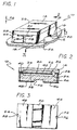
- FIG. 1 is a perspective view of an accelerometer embodying the present invention;
- FIG. 2 is a transverse cross-sectional view taken generally along the plane defined by section arrows 2-2-2 of FIG. 1, and viewed in the direction of the arrows;
- FIG. 3 provides a view of the underside, or mounting surface, of the accelerator seen in FIG. 1, as is represented by the arrows 3-3 of the latter Figure; and
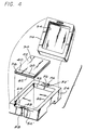
- FIG. 4 is an exploded perspective view of component parts of the present accelerometer preparatory to their assembly into a complete accelerometer.
- Viewing the drawing Figures in conjunction, and particularly FIG. 1, an accelerometer 10 is depicted mounted upon a printed circuit board 12 (only a fragment of which is depicted). The accelerometer 10 includes a housing, generally referenced with the
numeral 14, which secures upon and is electrically connected to a pair ofmetallic mounting pads 16, 18 of thecircuit board 12. A pair of metallicprinted circuit elements 20,22 extended respectively from the pads to other electrical circuitry of thecircuit board 12. - Considering the accelerometer 10 more closely, and particularly the
housing 14 thereof, it will be seen that the latter includes aceramic base portion 24 and aceramic top portion 26 which are adhesively intersecured along aninterface plane 28, which interface plane appears as a joint line on the outer surface of thehousing 14. Captured between thehousing portions interface plane 28, is a bimorph piezoceramic element orbeam 30, only a portion of which is visible viewing FIG. 1. - FIG. 2 shows that each of the
housing portions recesses cavity 36 receiving thepiezoceramic element 30. The piezoceramic element is a bimorph, meaning it is a laminated piezoceramic of two opposite-polarity ceramic portions electrically and physical intersecured with conductive adhesive therebetween. This bimorph piezoceramic structure is well-known, and so will not be further described except to point out thelamination plane 38 whereat the piezo ceramic portions are interbonded. Thepiezoceramic element 30 is a rectangular prismatic solid, as is best seen viewing FIG. 4, and is captured at amarginal edge portion 40 thereof between thehousing portions cantilever portion 42 of thepiezoceramic element 30 extends in thecavity 36 in spaced relation with the remainder of thehousing 14. - Viewing FIG. 3, it will be seen that the lower, or mounting, face of the accelerometer 10, which is generally referenced with the
numeral 44 and arrow, includes a pair ofmetallized surface portions 46, 48. Thesurface portions 46, 48 comprise the entirelower surface 44 of thehousing 14, with the exception of a transectinggroove 50 extending from one side to the other of thehousing 14. In fact, thesurface portions 46, 48 are defined by a surface metallization on theceramic housing portion 24, which metallization is so thin that it is not distinguished from the material of thehousing portion 24 except by heavy-weight line on the drawing Figures. Thesurface metallizations 46, 48 are not continuous acrossgroove 50. By use of a conductive epoxy adhesive applied at thesurface portions 46, 48, the accelerometer 10 may be securely mounted to, and electrically connected with, themounting pads 16, 18 of thecircuit board 12. Electrically connecting with therespective surface metallizations 46, 48 aresurface metallization portions respective grooves base portion 24. - The exploded perspective view of FIG. 4 shows that the
piezoceramic element 30 carries a pair ofsurface metallizations 60, 62 (only one of which is visible in FIG. 4) completely covering the opposite sides thereof including themarginal edge portion 40. Thesurface metallizations piezoceramic element 30. Thehousing portion 24 defines aseat 64 in the form of a groove opening outwardly fromrecess 32 and into which themarginal edge portion 40 ofpiezoceramic element 30 is received. Theseat 64 is substantially equal in depth, with respect to aplanar interface surface 66 of thehousing portion 24, as the thickness of themarginal edge portion 40. - In order to insure electrical conductivity of the
surface metallization 62 with mounting surface metallization 48 (via metallization 54) an area ofsurface metallization 54′ is provided inseat groove 64 and electrically continuous with themetallization 54 ingroove 58. Also, a region ofconductive epoxy 68 is applied at the juncture ofgroove 58 andmetallization 62 upon thearea 54′ of surface metallization. The remainder ofseat 64 is surfaced with an interface layer of structural epoxy (not illustrated) so that theelement 30 is secured in theseat 64. As secured into theseat 64, theelement 30 is disposed withsurface metallization 60 at the level ofinterface surface 66. - Similarly, in order to provide electrical connection of the
surface metallization 60 with mounting surface metallization 46, thetop portion 26 carries a peripheral surface metallization 70 circumscribing therecess 34 and defining an interfacesurface confronting surface 66. At thegroove 56, thesurface metallization 52 is carried ontosurface 66 to define an area of surface metallization referenced withnumeral 52′. Disposed upon the surface metallization 70 in congruence withsurface metallization 60 of thepiezoceramic element 30, is a region of conductive epoxy 72. At the opposite end of thehousing 14, a region of conductive epoxy 74 connects surface metallization 70 with themetallization 52′. The remainder of surface 70 is bonded to surface 66 (including thesurface 60 of piezoceramic element 30) using a structural epoxy to effect sealing and structural integrity ofhousing 14. - Having observed the structure of the accelerometer 10, attention may now be turned to its operation. Viewing FIG. 1 once again, the accelerometer 10 is adhesively secured and electrically connected to the
pads 16, 18 oncircuit board 12 by conductive epoxy between the pads and thesurface metallizations 46, 48 of the accelerometer housing. Consequently, when an acceleration (represented by arrow 76 viewing FIG. 1) is applied to thecircuit board 12 along a vector perpendicular thereto, the beam-likepiezoceramic element 30 flexes in response to the acceleration force. As is well-known in the art, the flexure of the two opposite-polarity piezo crystals of thebimorph element 30 results in an electrical charge across the opposite faces of the crystal. In thepiezoceramic element 30, these opposite charges are collected at thesurface metallizations - From the
surface metallization 62, the electrical charge is conducted via theconductive epoxy 68 tometallization 54′ ingroove 64 andmetallization 54 ingroove 58, and thence tosurface metallization 48 on themounting face 44 of the accelerometer. Likewise, from thesurface metallization 60, the electrical charge is conducted via conductive epoxy 72 into the peripheral metallization 70 circumscribing therecess 34. As noted earlier, the surface metallization 70 is electrically connected by conductive epoxy 74 to themetallization 52′ onsurface 66 and tometallization 52 ingroove 56. Therefore, the electrical charge frommetallization 60 ofelement 30 is conducted to surface metallization 46 on the mountingface 44. - An important feature of the accelerometer herein described is its inherently low capacitance. As can easily be appreciated, the
piezoceramic element 30 provides electrical charge in response to stressing of the piezoceramic portions thereof. Were the electrical connections between thepiezoceramic element 30 and measurement circuitry external to the accelerometer to provide a high capacitance, the produced charge would simply be absorbed in large part into this capacitance. Therefore, it is important to note that the structure of accelerometer 10 is substantially free of capacitance-forming features. For example, thesections 46 and 48 of surface metallization because of their spaced apart and edge-on orientation minimize the capacitance resulting from these metallization areas. Only a relatively small fraction of thesurface metallization 48 is in spaced apart face-to-face confronting relation with a portion of the surface metallization 70. However, the area of the surface metallization 70 in confronting relation withmetallization 48 is very small. Consequently, accelerometers embodying the present invention have shown an internal capacitance of about 550 pF, with a charge sensitivity to acceleration along the principle axis of 2.00 pC/g. (1g = 9,81 m/s²) This combination of charge sensitivity and low internal capacitance results in an electrical output from the accelerometer 10 which is easily accommodated by measurement circuitry external to the accelerometer. - The present accelerometer is seen to fulfill all of the objectives set out above. The structure of the accelerometer is straightforward, comparatively inexpensive to manufacture, rugged and reliable in use, and is easily handled with modern SMT manufacturing techniques. Accelerometers embodying the present invention will survive 5000 g (1g = 9,81 m/s²) without damage. Yet, should the
cantilever portion 42 of thebeam 30 break off, thehousing 14 completely contains this fractured part so that it does not present a potential short circuit element for other electrical circuitry neighboring the accelerometer. While the invention has been depicted and described by reference to one particularly preferred embodiment thereof, such reference does not imply a limitation upon the invention, and no such limitation is to be inferred. The invention is intended to be limited only by the scope of the appended claims, which provide additional definition of the invention.
Claims (12)
- A cantilever beam surface-mount piezoceramic accelerometer (10) comprising:
a housing (14) of glass or ceramic defining a cavity (36) therewithin, a mounting face (44), and a pair of spaced apart surface electrical contacts (46, 48) disposed on said mounting face of said housing;
a piezoceramic beam (30) having a marginal edge portion (40) securing to said housing and a cantilever portion (42) freely extending within said cavity, said piezoceramic beam including a respective pair of electrical contacts (60, 62) on opposite sides thereof at said marginal edge portion;
said housing including electrical conduction means (46, 48, 52, 54, 70) for connecting each of said pair of electrical contacts of said piezoceramic beam with a respective one of said pair of surface electrical contacts of said housing;
wherein said electrical conduction means includes an externally disposed surface metallization (52, 54) at one end connecting with a respective one of said pair of surface electrical contacts (46, 48) of said housing and at the other end connecting electrically with one of said pair of electrical contacts (60, 62) of said piezoceramic beam. - The invention of Claim 1 wherein said externally disposed surface metallization is disposed in a groove (56, 58) outwardly defined by said housing (14) and extending generally perpendicularly to said one of said pair of surface electrical contacts (46, 48) of said housing to intersect therewith.
- The invention of Claim 1 wherein said housing includes a base portion (24) and a top portion (26) intersecuring along an interface plane (28), said electrical conduction means including a metallic surface (70) at said interface plane and carried by one of said housing portions.
- The invention of Claim 3 wherein said base (24) portion defines a seat (64) communicating with said cavity (36), said piezoceramic beam (30) being received in said seat with the one (60) of said pair of surface contacts (60, 62) thereof which is disposed away from said base portion substantially in said interface plane.
- The invention of Claim 4 wherein said top portion (26) carries said metallic surface (70) at said interface plane in confronting relation with said one surface contact (60) of said piezoceramic beam.
- The invention of Claim 5 wherein said metallic surface (70) is defined by a surface metallization carried by said housing top portion of said interface plane.
- The invention of Claim 1 wherein said housing (14) includes a base portion (24) carrying said surface electrical contacts (46, 48), and a top portion (26) cooperating with said base portion to capture said piezoceramic beam (30) therebetween, each of said base portion and said top portion of said housing defining a respective one of a pair of recesses (32, 34) opening on opposite sides of said piezoceramic beam, and said pair of recesses cooperatively defining said cavity (36).
- A piezoceramic surface-mount accelerometer (10) comprising:
a chambered rectangular prismatic housing (14) of glass or ceramic including a solid base portion (24) having a lower mounting surface (44) which is divided into a pair of surface-contact areas (46, 48) by a transverse groove (50) defined thereon, a surface metallization (46, 48) carried upon each of said surface-contact areas to define a pair of surface electrical contacts for said accelerometer, a pair of vertical grooves (56, 58) defined by said base portion and each extending upwardly along opposite end surfaces of said housing and each at lower ends thereof intersecting with a respective one of the pair of surface contact areas (46, 48) of said housing, surface metallization (52, 54) extending the entire length of each of said pair of vertical grooves to at the lower end thereof electrically connect with a respective one of said pair of surface electrical contacts (46, 48), said base portion defining a respective recess (32) opening upwardly thereon to define an upwardly disposed peripheral interface surface (66) circumscribing said recess, a seat groove (64) extending transversely to open outwardly from said base portion recess across said interface surface at an end surface of said housing in intersection with one (58) of said vertical grooves (56, 58);
a bimorph piezoceramic beam (30) received at a marginal edge portion (40) thereof into said seat groove (64) with an upper face thereof in alignment with said interface surface (66), said beam including a pair of oppositely disposed upper-surface and lower-surface surface metallization electrical contacts (60, 62) at said marginal edge portion, said lower-surface electrical contact (62) being in electrical continuity with said surface metallization (54) at said one end groove (58), and said beam including a cantilevered free portion (42) extending into said base portion recess in spaced relation with the remainder of said base portion; and
a prismatic solid housing top portion (26) congruent with said base portion, said top portion defining a recess (34) opening downardly and defining a peripheral surface (70), said top portion recess and peripheral surface being congruent with and confronting said base portion recess and interface surface, a surface metallization (70) carried upon said peripheral surface and extending about said recess from one end thereof to the other, said top portion securing at said peripheral surface thereof to said base portion on said interface surface (66), and said surface metallization of said top portion being in electrical continuity with both said upper-surface electrical contact (60) of said piezoceramic beam and said surface metallization (52) in the other (56) of said pair of grooves (56, 58). - The invention of Claim 8 wherein electrical continuities between said lower-surface and said upper surface electrical contacts (60, 62) of said piezoceramic beam, said surface metallizations (52, 54) in said pair of vertical grooves (56, 58) of said base portion, and said surface metallization (70) carried upon said peripheral surface of said top portion, are all effected by use of controlled areas of conductive epoxy (68).
- The invention of Claim 9 wherein said piezoceramic beam (30) is mounted into said seat groove (64), and said top portion (26) is secured to said base portion (24) to trap said beam within said housing chamber (36) and seal the latter, all with structural epoxy.
- A method of providing a piezoceramic accelerometer (10) for surface mount upon a circuit board (12), said method comprising the steps of:
forming a housing (14) base portion (24) and a congruent housing top portion (26) each as prismatic solids of ceramic or glass material, providing on each of said base portion and top portion a respective one of a pair of recesses (32, 34) which in confronting congruence with the other of the pair of recesses cooperate to define both a chamber (36) within said housing (14) and a respective peripheral surface (66, 70) circumscribing said recess of each portion, on a lower mounting surface of said housing base portion providing a pair of surface-contact areas (46, 48), providing a pair of vertical grooves (56, 58) at end surfaces of said base portion intersecting with respective ones of said pair of surface-contact areas (46, 48), and forming a seat groove (64) traversing said peripheral surface (66) of said base portion outwardly of said recess thereof to intersect one of said pair of vertical grooves;
forming a piezoceramic bimorph beam (30) having a marginal edge portion (40) receivable into said seat groove (64) and a free cantilever portion (42) extensible into said chamber (36);
providing electrically conductive surface metallization (46, 48) on all of said pair of surface contact areas, said pair of vertical grooves (56, 58), said peripheral surface (70) of said housing top portion, and opposite sides (60, 62) of said marginal edge portion of said piezoceramic beam; and
capturing said piezoceramic beam (30) in said seat groove (64) and chamber (36) between said housing base portion (24) and top portion (26). - The method of Claim 11 further including the step of employing respective areas of conductive epoxy (68) to insure electrical continuity between:
one (62) of the said opposite side surface metallizations (60, 62) of said piezoceramic beam and the surface metallization (54) of said one vertical groove intersecting said seat groove (64);
the other (60) of said opposite side surface metallizations of said piezoceramic beam and said peripheral surface metallization (70) of said housing top portion; and
said peripheral surface metallization (70) of said housing top portion and the surface metallization (52) of other of said pair of vertical grooves.
Applications Claiming Priority (3)
| Application Number | Priority Date | Filing Date | Title |
|---|---|---|---|
| US47978790A | 1990-02-14 | 1990-02-14 | |
| US479787 | 1990-02-14 | ||
| PCT/US1991/000654 WO1991013364A2 (en) | 1990-02-14 | 1991-01-31 | Surface-mount piezoceramic accelerometer and method for making same |
Publications (2)
| Publication Number | Publication Date |
|---|---|
| EP0515521A1 EP0515521A1 (en) | 1992-12-02 |
| EP0515521B1 true EP0515521B1 (en) | 1994-09-28 |
Family
ID=23905436
Family Applications (1)
| Application Number | Title | Priority Date | Filing Date |
|---|---|---|---|
| EP91904876A Expired - Lifetime EP0515521B1 (en) | 1990-02-14 | 1991-01-31 | Surface-mount piezoceramic accelerometer and method for making same |
Country Status (5)
| Country | Link |
|---|---|
| US (1) | US5235237A (en) |
| EP (1) | EP0515521B1 (en) |
| JP (1) | JP3091766B2 (en) |
| DE (1) | DE69104349T2 (en) |
| WO (1) | WO1991013364A2 (en) |
Cited By (3)
| Publication number | Priority date | Publication date | Assignee | Title |
|---|---|---|---|---|
| DE10137424A1 (en) * | 2001-07-27 | 2003-04-24 | Holmberg Gmbh & Co Kg | Piezoelectric element for converting pressure signals into electrical signals and vice versa comprises a ceramic body with open pores and elastic coating |
| US6897601B2 (en) | 2001-07-27 | 2005-05-24 | Holmberg Gmbh & Co. Kg | Piezoelectric element and an oscillation transducer with a piezoelectric element |
| DE102022134075A1 (en) * | 2022-12-20 | 2024-06-20 | Physik Instrumente (PI) GmbH & Co KG | Drive system and control method for a piezoelectric motor |
Families Citing this family (47)
| Publication number | Priority date | Publication date | Assignee | Title |
|---|---|---|---|---|
| US5481184A (en) * | 1991-12-31 | 1996-01-02 | Sarcos Group | Movement actuator/sensor systems |
| JP3141954B2 (en) * | 1991-07-17 | 2001-03-07 | 株式会社ワコー | Force / acceleration / magnetism sensors using piezoelectric elements |
| US5345823A (en) * | 1991-11-12 | 1994-09-13 | Texas Instruments Incorporated | Accelerometer |
| US5334901A (en) * | 1993-04-30 | 1994-08-02 | Alliedsignal Inc. | Vibrating beam accelerometer |
| DE9314084U1 (en) * | 1993-09-17 | 1994-01-05 | Mannesmann Kienzle Gmbh, 78052 Villingen-Schwenningen | Arrangement for attaching a micromechanical sensor to a carrier by gluing |
| US5539270A (en) * | 1993-11-19 | 1996-07-23 | Matsushita Electric Works, Ltd. | Acceleration detector |
| US5514927A (en) * | 1994-02-28 | 1996-05-07 | Motorola, Inc. | Piezoelectric audio transducer |
| DE4428124B4 (en) * | 1994-08-09 | 2005-08-18 | Robert Bosch Gmbh | accelerometer |
| DE4439297A1 (en) * | 1994-11-07 | 1996-05-09 | Pi Ceramic Gmbh | Piezoelectric sensor with beam or plate type element with linear and width edges |
| DE4440078A1 (en) * | 1994-11-10 | 1996-05-15 | Telefunken Microelectron | Piezoelectric accelerometer |
| US5835077A (en) * | 1995-01-13 | 1998-11-10 | Remec, Inc., | Computer control device |
| US5581034A (en) * | 1995-01-13 | 1996-12-03 | Remec, Inc. | Convective accelerometer and inclinometer |
| US5808197A (en) * | 1995-01-13 | 1998-09-15 | Remec, Inc. | Vehicle information and control system |
| US5911738A (en) * | 1997-07-31 | 1999-06-15 | Medtronic, Inc. | High output sensor and accelerometer implantable medical device |
| US5674258A (en) * | 1995-03-08 | 1997-10-07 | Medtronic, Inc. | Packaged integrated accelerometer |
| US6043588A (en) * | 1995-07-18 | 2000-03-28 | Murata Manufacturing Co., Ltd. | Piezoelectric sensor and acceleration sensor |
| US6976295B2 (en) | 1997-07-29 | 2005-12-20 | Seiko Epson Corporation | Method of manufacturing a piezoelectric device |
| US6960870B2 (en) * | 1997-07-29 | 2005-11-01 | Seiko Epson Corporation | Piezo-electric resonator and manufacturing method thereof |
| DE19745311C1 (en) * | 1997-10-14 | 1999-07-01 | Telefunken Microelectron | Piezoelectric bending sensor accelerometer |
| US5983722A (en) * | 1997-11-12 | 1999-11-16 | K.K. Holding Ag | Piezobloc accelerometer |
| AUPP130498A0 (en) * | 1998-01-12 | 1998-02-05 | Griffith University | Monitoring arrangement for a multi-element boom |
| US6101877A (en) * | 1998-01-13 | 2000-08-15 | Maytag Corporation | Accelerometer mounting |
| JP3887137B2 (en) * | 1999-01-29 | 2007-02-28 | セイコーインスツル株式会社 | Method for manufacturing piezoelectric vibrator |
| US6216537B1 (en) | 1999-03-31 | 2001-04-17 | Medtronic, Inc. | Accelerometer for implantable medical device |
| JP2001060843A (en) * | 1999-08-23 | 2001-03-06 | Murata Mfg Co Ltd | Chip type piezoelectric part |
| WO2001014890A1 (en) * | 1999-08-24 | 2001-03-01 | Koninklijke Philips Electronics N.V. | Accelerometer and method of manufacturing same |
| US6522914B1 (en) * | 2000-07-14 | 2003-02-18 | Cardiac Pacemakers, Inc. | Method and apparatuses for monitoring hemodynamic activities using an intracardiac impedance-derived parameter |
| JP2003318699A (en) * | 2002-04-23 | 2003-11-07 | Piedekku Gijutsu Kenkyusho:Kk | Crystal unit and its manufacturing method |
| US7092757B2 (en) | 2002-07-12 | 2006-08-15 | Cardiac Pacemakers, Inc. | Minute ventilation sensor with dynamically adjusted excitation current |
| JP4602080B2 (en) | 2002-07-25 | 2010-12-22 | ボストン サイエンティフィック リミテッド | Medical devices that travel through the human body structure |
| US7101339B2 (en) | 2002-12-13 | 2006-09-05 | Cardiac Pacemakers, Inc. | Respiration signal measurement apparatus, systems, and methods |
| US7001369B2 (en) | 2003-03-27 | 2006-02-21 | Scimed Life Systems, Inc. | Medical device |
| US7200440B2 (en) | 2003-07-02 | 2007-04-03 | Cardiac Pacemakers, Inc. | Cardiac cycle synchronized sampling of impedance signal |
| US7516660B2 (en) * | 2004-05-21 | 2009-04-14 | Met Tech, Inc. | Convective accelerometer |
| US7259499B2 (en) * | 2004-12-23 | 2007-08-21 | Askew Andy R | Piezoelectric bimorph actuator and method of manufacturing thereof |
| US20080072671A1 (en) * | 2006-09-26 | 2008-03-27 | Eldon Eller | Leveraged shear mode accelerometers |
| US8556914B2 (en) | 2006-12-15 | 2013-10-15 | Boston Scientific Scimed, Inc. | Medical device including structure for crossing an occlusion in a vessel |
| KR100856293B1 (en) * | 2007-05-04 | 2008-09-03 | 삼성전기주식회사 | Manufacturing Method of Crystal Oscillator |
| KR100878410B1 (en) * | 2007-07-11 | 2009-01-13 | 삼성전기주식회사 | Manufacturing Method of Crystal Oscillator |
| US9808595B2 (en) | 2007-08-07 | 2017-11-07 | Boston Scientific Scimed, Inc | Microfabricated catheter with improved bonding structure |
| WO2011043219A1 (en) | 2009-10-07 | 2011-04-14 | Necトーキン株式会社 | Piezoelectric acceleration sensor |
| JP2015034755A (en) * | 2013-08-09 | 2015-02-19 | セイコーエプソン株式会社 | Sensor unit, electronic apparatus, and moving body |
| US9470806B2 (en) * | 2013-08-29 | 2016-10-18 | Pgs Geophysical As | Piezoelectric accelerometer |
| US9901706B2 (en) | 2014-04-11 | 2018-02-27 | Boston Scientific Scimed, Inc. | Catheters and catheter shafts |
| US11351048B2 (en) | 2015-11-16 | 2022-06-07 | Boston Scientific Scimed, Inc. | Stent delivery systems with a reinforced deployment sheath |
| RU2621467C1 (en) * | 2016-06-30 | 2017-06-06 | Акционерное общество "Научно-исследовательский институт "Элпа" с опытным производством" | Small sensor of shock |
| US20250258193A1 (en) * | 2024-02-09 | 2025-08-14 | Industrial Consulting Automation Research Engineering SRL | Method and apparatus for automated production of piezoelectric accelerometers |
Family Cites Families (18)
| Publication number | Priority date | Publication date | Assignee | Title |
|---|---|---|---|---|
| US3047749A (en) * | 1959-08-05 | 1962-07-31 | Midland Mfg Co Inc | Miniaturized piezoelectric crystal apparatus and method of making same |
| US3113223A (en) * | 1960-07-27 | 1963-12-03 | Space Technology Lab Inc | Bender-type accelerometer |
| JPS5613719U (en) * | 1979-07-13 | 1981-02-05 | ||
| US4421621A (en) * | 1979-07-17 | 1983-12-20 | Kabushiki Kaisha Suwa Seikosha | Quartz crystal oscillator |
| US4405875A (en) * | 1980-07-24 | 1983-09-20 | Kiyoshi Nagai | Hermetically sealed flat-type piezo-electric oscillator assembly |
| US4346597A (en) * | 1980-11-03 | 1982-08-31 | United Technologies Corporation | Dual range, cantilevered mass accelerometer |
| US4750031A (en) * | 1982-06-25 | 1988-06-07 | The United States Of America As Represented By The United States National Aeronautics And Space Administration | Hermetically sealable package for hybrid solid-state electronic devices and the like |
| AT380934B (en) * | 1983-01-13 | 1986-07-25 | Enfo Grundlagen Forschungs Ag | ELECTRICAL-PNEUMATIC SIGNAL CONVERTER |
| EP0127442B1 (en) * | 1983-05-30 | 1991-04-17 | Fujitsu Limited | Piezoelectric resonator |
| CH655423GA3 (en) * | 1984-02-15 | 1986-04-30 | ||
| EP0175508B1 (en) * | 1984-09-07 | 1988-10-12 | The Marconi Company Limited | Vibrational gyroscope |
| US4639631A (en) * | 1985-07-01 | 1987-01-27 | Motorola, Inc. | Electrostatically sealed piezoelectric device |
| US4679434A (en) | 1985-07-25 | 1987-07-14 | Litton Systems, Inc. | Integrated force balanced accelerometer |
| DE3539504A1 (en) * | 1985-11-07 | 1987-05-21 | Schott Glaswerke | FLAT HOUSING FOR THE HERMETIC ENCLOSURE OF PIEZOELECTRIC COMPONENTS |
| US4694687A (en) * | 1986-04-17 | 1987-09-22 | Vericom Corporation | Vehicle performance analyzer |
| US4734068A (en) * | 1986-07-11 | 1988-03-29 | The Eska Company | Mounting structure for electric trolling motors |
| DE3819050A1 (en) * | 1988-06-04 | 1989-12-14 | Bosch Gmbh Robert | SAFETY CIRCUIT FOR ELECTRIC HAND TOOLS |
| EP0351038A1 (en) * | 1988-06-10 | 1990-01-17 | Hewlett-Packard Company | Improved accelerometer and method of manufacture |
-
1991
- 1991-01-31 WO PCT/US1991/000654 patent/WO1991013364A2/en not_active Ceased
- 1991-01-31 JP JP03504681A patent/JP3091766B2/en not_active Expired - Lifetime
- 1991-01-31 DE DE69104349T patent/DE69104349T2/en not_active Expired - Fee Related
- 1991-01-31 EP EP91904876A patent/EP0515521B1/en not_active Expired - Lifetime
- 1991-12-04 US US07/803,701 patent/US5235237A/en not_active Expired - Lifetime
Cited By (4)
| Publication number | Priority date | Publication date | Assignee | Title |
|---|---|---|---|---|
| DE10137424A1 (en) * | 2001-07-27 | 2003-04-24 | Holmberg Gmbh & Co Kg | Piezoelectric element for converting pressure signals into electrical signals and vice versa comprises a ceramic body with open pores and elastic coating |
| DE10137424C2 (en) * | 2001-07-27 | 2003-07-31 | Holmberg Gmbh & Co Kg | vibration transducer |
| US6897601B2 (en) | 2001-07-27 | 2005-05-24 | Holmberg Gmbh & Co. Kg | Piezoelectric element and an oscillation transducer with a piezoelectric element |
| DE102022134075A1 (en) * | 2022-12-20 | 2024-06-20 | Physik Instrumente (PI) GmbH & Co KG | Drive system and control method for a piezoelectric motor |
Also Published As
| Publication number | Publication date |
|---|---|
| EP0515521A1 (en) | 1992-12-02 |
| DE69104349D1 (en) | 1994-11-03 |
| US5235237A (en) | 1993-08-10 |
| JP3091766B2 (en) | 2000-09-25 |
| JPH05505236A (en) | 1993-08-05 |
| WO1991013364A3 (en) | 1991-10-03 |
| WO1991013364A2 (en) | 1991-09-05 |
| DE69104349T2 (en) | 1995-05-24 |
Similar Documents
| Publication | Publication Date | Title |
|---|---|---|
| EP0515521B1 (en) | Surface-mount piezoceramic accelerometer and method for making same | |
| US4891984A (en) | Acceleration detecting apparatus formed by semiconductor | |
| US5515725A (en) | Piezoelectric bimorph type acceleration sensor | |
| US5433110A (en) | Detector having selectable multiple axes of sensitivity | |
| US8103025B2 (en) | Surface mountable transducer system | |
| US4896068A (en) | Activity sensor for a heart pacemaker | |
| US4836023A (en) | Vibrational angular rate sensor | |
| EP0638783B1 (en) | Rotation rate sensor with center mounted tuning fork | |
| JP3401790B2 (en) | Acceleration sensor and acceleration device using this acceleration sensor | |
| JPH03183963A (en) | Accelerometer | |
| WO2003001150A1 (en) | Composite sensor for detecting angular velocity and acceleration | |
| US7134339B2 (en) | Acceleration sensor | |
| US5631421A (en) | Piezoelectric acceleration transducer | |
| US5388459A (en) | Acceleration sensor with direct mounting | |
| US12461122B2 (en) | Multi-axis inertial force sensor | |
| US6321600B1 (en) | Acceleration detecting device | |
| TW202028939A (en) | Force sensor | |
| CA2242415C (en) | Acceleration sensor | |
| US5983722A (en) | Piezobloc accelerometer | |
| JP3106970B2 (en) | Acceleration sensor | |
| JPH04130670A (en) | Electrostatic capacitance type pressure sensor | |
| CN101218669A (en) | Electronic component manufacturing method and electronic component | |
| JP3342748B2 (en) | Acceleration sensor | |
| JP3111858B2 (en) | Piezoelectric sensor | |
| JPH07202283A (en) | Piezoelectric sensor and its manufacture |
Legal Events
| Date | Code | Title | Description |
|---|---|---|---|
| PUAI | Public reference made under article 153(3) epc to a published international application that has entered the european phase |
Free format text: ORIGINAL CODE: 0009012 |
|
| 17P | Request for examination filed |
Effective date: 19920903 |
|
| AK | Designated contracting states |
Kind code of ref document: A1 Designated state(s): DE FR GB |
|
| RAP1 | Party data changed (applicant data changed or rights of an application transferred) |
Owner name: ENDEVCO CORPORATION |
|
| 17Q | First examination report despatched |
Effective date: 19931208 |
|
| GRAA | (expected) grant |
Free format text: ORIGINAL CODE: 0009210 |
|
| AK | Designated contracting states |
Kind code of ref document: B1 Designated state(s): DE FR GB |
|
| REF | Corresponds to: |
Ref document number: 69104349 Country of ref document: DE Date of ref document: 19941103 |
|
| ET | Fr: translation filed | ||
| PG25 | Lapsed in a contracting state [announced via postgrant information from national office to epo] |
Ref country code: GB Effective date: 19950131 |
|
| PLBE | No opposition filed within time limit |
Free format text: ORIGINAL CODE: 0009261 |
|
| STAA | Information on the status of an ep patent application or granted ep patent |
Free format text: STATUS: NO OPPOSITION FILED WITHIN TIME LIMIT |
|
| 26N | No opposition filed | ||
| GBPC | Gb: european patent ceased through non-payment of renewal fee |
Effective date: 19950131 |
|
| PG25 | Lapsed in a contracting state [announced via postgrant information from national office to epo] |
Ref country code: FR Effective date: 19950929 |
|
| PG25 | Lapsed in a contracting state [announced via postgrant information from national office to epo] |
Ref country code: DE Effective date: 19951003 |
|
| REG | Reference to a national code |
Ref country code: FR Ref legal event code: ST |