EP0544439A1 - Gegenstand mit einem spannungsverformten Quantumwell-Laser - Google Patents
Gegenstand mit einem spannungsverformten Quantumwell-Laser Download PDFInfo
- Publication number
- EP0544439A1 EP0544439A1 EP92310489A EP92310489A EP0544439A1 EP 0544439 A1 EP0544439 A1 EP 0544439A1 EP 92310489 A EP92310489 A EP 92310489A EP 92310489 A EP92310489 A EP 92310489A EP 0544439 A1 EP0544439 A1 EP 0544439A1
- Authority
- EP
- European Patent Office
- Prior art keywords
- layer
- blocking layer
- semiconductor
- article
- laser
- Prior art date
- Legal status (The legal status is an assumption and is not a legal conclusion. Google has not performed a legal analysis and makes no representation as to the accuracy of the status listed.)
- Granted
Links
Images


Classifications
-
- H—ELECTRICITY
- H01—ELECTRIC ELEMENTS
- H01S—DEVICES USING THE PROCESS OF LIGHT AMPLIFICATION BY STIMULATED EMISSION OF RADIATION [LASER] TO AMPLIFY OR GENERATE LIGHT; DEVICES USING STIMULATED EMISSION OF ELECTROMAGNETIC RADIATION IN WAVE RANGES OTHER THAN OPTICAL
- H01S5/00—Semiconductor lasers
- H01S5/20—Structure or shape of the semiconductor body to guide the optical wave ; Confining structures perpendicular to the optical axis, e.g. index or gain guiding, stripe geometry, broad area lasers, gain tailoring, transverse or lateral reflectors, special cladding structures, MQW barrier reflection layers
- H01S5/22—Structure or shape of the semiconductor body to guide the optical wave ; Confining structures perpendicular to the optical axis, e.g. index or gain guiding, stripe geometry, broad area lasers, gain tailoring, transverse or lateral reflectors, special cladding structures, MQW barrier reflection layers having a ridge or stripe structure
- H01S5/223—Buried stripe structure
- H01S5/2231—Buried stripe structure with inner confining structure only between the active layer and the upper electrode
-
- B—PERFORMING OPERATIONS; TRANSPORTING
- B82—NANOTECHNOLOGY
- B82Y—SPECIFIC USES OR APPLICATIONS OF NANOSTRUCTURES; MEASUREMENT OR ANALYSIS OF NANOSTRUCTURES; MANUFACTURE OR TREATMENT OF NANOSTRUCTURES
- B82Y20/00—Nanooptics, e.g. quantum optics or photonic crystals
-
- H—ELECTRICITY
- H01—ELECTRIC ELEMENTS
- H01S—DEVICES USING THE PROCESS OF LIGHT AMPLIFICATION BY STIMULATED EMISSION OF RADIATION [LASER] TO AMPLIFY OR GENERATE LIGHT; DEVICES USING STIMULATED EMISSION OF ELECTROMAGNETIC RADIATION IN WAVE RANGES OTHER THAN OPTICAL
- H01S5/00—Semiconductor lasers
- H01S5/20—Structure or shape of the semiconductor body to guide the optical wave ; Confining structures perpendicular to the optical axis, e.g. index or gain guiding, stripe geometry, broad area lasers, gain tailoring, transverse or lateral reflectors, special cladding structures, MQW barrier reflection layers
- H01S5/22—Structure or shape of the semiconductor body to guide the optical wave ; Confining structures perpendicular to the optical axis, e.g. index or gain guiding, stripe geometry, broad area lasers, gain tailoring, transverse or lateral reflectors, special cladding structures, MQW barrier reflection layers having a ridge or stripe structure
- H01S5/2205—Structure or shape of the semiconductor body to guide the optical wave ; Confining structures perpendicular to the optical axis, e.g. index or gain guiding, stripe geometry, broad area lasers, gain tailoring, transverse or lateral reflectors, special cladding structures, MQW barrier reflection layers having a ridge or stripe structure comprising special burying or current confinement layers
- H01S5/2218—Structure or shape of the semiconductor body to guide the optical wave ; Confining structures perpendicular to the optical axis, e.g. index or gain guiding, stripe geometry, broad area lasers, gain tailoring, transverse or lateral reflectors, special cladding structures, MQW barrier reflection layers having a ridge or stripe structure comprising special burying or current confinement layers having special optical properties
- H01S5/2219—Structure or shape of the semiconductor body to guide the optical wave ; Confining structures perpendicular to the optical axis, e.g. index or gain guiding, stripe geometry, broad area lasers, gain tailoring, transverse or lateral reflectors, special cladding structures, MQW barrier reflection layers having a ridge or stripe structure comprising special burying or current confinement layers having special optical properties absorbing
-
- H—ELECTRICITY
- H01—ELECTRIC ELEMENTS
- H01S—DEVICES USING THE PROCESS OF LIGHT AMPLIFICATION BY STIMULATED EMISSION OF RADIATION [LASER] TO AMPLIFY OR GENERATE LIGHT; DEVICES USING STIMULATED EMISSION OF ELECTROMAGNETIC RADIATION IN WAVE RANGES OTHER THAN OPTICAL
- H01S5/00—Semiconductor lasers
- H01S5/20—Structure or shape of the semiconductor body to guide the optical wave ; Confining structures perpendicular to the optical axis, e.g. index or gain guiding, stripe geometry, broad area lasers, gain tailoring, transverse or lateral reflectors, special cladding structures, MQW barrier reflection layers
- H01S5/22—Structure or shape of the semiconductor body to guide the optical wave ; Confining structures perpendicular to the optical axis, e.g. index or gain guiding, stripe geometry, broad area lasers, gain tailoring, transverse or lateral reflectors, special cladding structures, MQW barrier reflection layers having a ridge or stripe structure
- H01S5/2205—Structure or shape of the semiconductor body to guide the optical wave ; Confining structures perpendicular to the optical axis, e.g. index or gain guiding, stripe geometry, broad area lasers, gain tailoring, transverse or lateral reflectors, special cladding structures, MQW barrier reflection layers having a ridge or stripe structure comprising special burying or current confinement layers
- H01S5/2222—Structure or shape of the semiconductor body to guide the optical wave ; Confining structures perpendicular to the optical axis, e.g. index or gain guiding, stripe geometry, broad area lasers, gain tailoring, transverse or lateral reflectors, special cladding structures, MQW barrier reflection layers having a ridge or stripe structure comprising special burying or current confinement layers having special electric properties
- H01S5/2227—Structure or shape of the semiconductor body to guide the optical wave ; Confining structures perpendicular to the optical axis, e.g. index or gain guiding, stripe geometry, broad area lasers, gain tailoring, transverse or lateral reflectors, special cladding structures, MQW barrier reflection layers having a ridge or stripe structure comprising special burying or current confinement layers having special electric properties special thin layer sequence
-
- H—ELECTRICITY
- H01—ELECTRIC ELEMENTS
- H01S—DEVICES USING THE PROCESS OF LIGHT AMPLIFICATION BY STIMULATED EMISSION OF RADIATION [LASER] TO AMPLIFY OR GENERATE LIGHT; DEVICES USING STIMULATED EMISSION OF ELECTROMAGNETIC RADIATION IN WAVE RANGES OTHER THAN OPTICAL
- H01S5/00—Semiconductor lasers
- H01S5/20—Structure or shape of the semiconductor body to guide the optical wave ; Confining structures perpendicular to the optical axis, e.g. index or gain guiding, stripe geometry, broad area lasers, gain tailoring, transverse or lateral reflectors, special cladding structures, MQW barrier reflection layers
- H01S5/22—Structure or shape of the semiconductor body to guide the optical wave ; Confining structures perpendicular to the optical axis, e.g. index or gain guiding, stripe geometry, broad area lasers, gain tailoring, transverse or lateral reflectors, special cladding structures, MQW barrier reflection layers having a ridge or stripe structure
- H01S5/223—Buried stripe structure
- H01S5/2232—Buried stripe structure with inner confining structure between the active layer and the lower electrode
-
- H—ELECTRICITY
- H01—ELECTRIC ELEMENTS
- H01S—DEVICES USING THE PROCESS OF LIGHT AMPLIFICATION BY STIMULATED EMISSION OF RADIATION [LASER] TO AMPLIFY OR GENERATE LIGHT; DEVICES USING STIMULATED EMISSION OF ELECTROMAGNETIC RADIATION IN WAVE RANGES OTHER THAN OPTICAL
- H01S5/00—Semiconductor lasers
- H01S5/30—Structure or shape of the active region; Materials used for the active region
- H01S5/32—Structure or shape of the active region; Materials used for the active region comprising PN junctions, e.g. hetero- or double- heterostructures
- H01S5/3211—Structure or shape of the active region; Materials used for the active region comprising PN junctions, e.g. hetero- or double- heterostructures characterised by special cladding layers, e.g. details on band-discontinuities
-
- H—ELECTRICITY
- H01—ELECTRIC ELEMENTS
- H01S—DEVICES USING THE PROCESS OF LIGHT AMPLIFICATION BY STIMULATED EMISSION OF RADIATION [LASER] TO AMPLIFY OR GENERATE LIGHT; DEVICES USING STIMULATED EMISSION OF ELECTROMAGNETIC RADIATION IN WAVE RANGES OTHER THAN OPTICAL
- H01S5/00—Semiconductor lasers
- H01S5/30—Structure or shape of the active region; Materials used for the active region
- H01S5/34—Structure or shape of the active region; Materials used for the active region comprising quantum well or superlattice structures, e.g. single quantum well [SQW] lasers, multiple quantum well [MQW] lasers or graded index separate confinement heterostructure [GRINSCH] lasers
- H01S5/343—Structure or shape of the active region; Materials used for the active region comprising quantum well or superlattice structures, e.g. single quantum well [SQW] lasers, multiple quantum well [MQW] lasers or graded index separate confinement heterostructure [GRINSCH] lasers in AIIIBV compounds, e.g. AlGaAs-laser, InP-based laser
- H01S5/34306—Structure or shape of the active region; Materials used for the active region comprising quantum well or superlattice structures, e.g. single quantum well [SQW] lasers, multiple quantum well [MQW] lasers or graded index separate confinement heterostructure [GRINSCH] lasers in AIIIBV compounds, e.g. AlGaAs-laser, InP-based laser emitting light at a wavelength longer than 1000nm, e.g. InP based 1300 and 1500nm lasers
-
- H—ELECTRICITY
- H01—ELECTRIC ELEMENTS
- H01S—DEVICES USING THE PROCESS OF LIGHT AMPLIFICATION BY STIMULATED EMISSION OF RADIATION [LASER] TO AMPLIFY OR GENERATE LIGHT; DEVICES USING STIMULATED EMISSION OF ELECTROMAGNETIC RADIATION IN WAVE RANGES OTHER THAN OPTICAL
- H01S5/00—Semiconductor lasers
- H01S5/30—Structure or shape of the active region; Materials used for the active region
- H01S5/34—Structure or shape of the active region; Materials used for the active region comprising quantum well or superlattice structures, e.g. single quantum well [SQW] lasers, multiple quantum well [MQW] lasers or graded index separate confinement heterostructure [GRINSCH] lasers
- H01S5/343—Structure or shape of the active region; Materials used for the active region comprising quantum well or superlattice structures, e.g. single quantum well [SQW] lasers, multiple quantum well [MQW] lasers or graded index separate confinement heterostructure [GRINSCH] lasers in AIIIBV compounds, e.g. AlGaAs-laser, InP-based laser
- H01S5/34313—Structure or shape of the active region; Materials used for the active region comprising quantum well or superlattice structures, e.g. single quantum well [SQW] lasers, multiple quantum well [MQW] lasers or graded index separate confinement heterostructure [GRINSCH] lasers in AIIIBV compounds, e.g. AlGaAs-laser, InP-based laser with a well layer having only As as V-compound, e.g. AlGaAs, InGaAs
Definitions
- This invention pertains to strained-layer quantum well (QW) semiconductor lasers, and to articles that comprise such lasers.
- QW quantum well
- InP-based lasers can have emission wavelengths ⁇ 0.94 ⁇ m.
- InP-based lasers that have wavelengths in the short-wavelength portion (typically ⁇ 1 ⁇ m) of the wavelength regime accessible to such lasers typically have some disadvantageous features that make such lasers a poor choice for applications such as optical fiber amplifiers with pump radiation in the range 0.94 ⁇ m to about 1 ⁇ m.
- InP-based lasers that emit in that wavelength range typically have high threshold current and low quantum efficiency, due to their inherently low bandgap difference between InP and the relevant quaternary or ternary semiconductor alloy.
- the bandgap difference between GaAs and the relevant alloys is relatively large, making possible design of GaAs-based lasers having advantageous properties, e.g., relatively low threshold current and relatively small temperature dependence.
- the bandgaps of GaAs and the relevant alloys are such that all GaAs-based lattice matched lasers will have an emission wavelength that is ⁇ 0.87 ⁇ m.
- GaAs-based strained layer QW lasers that emit in the 0.87-1.1 ⁇ m wavelength regime are known. See, for instance, M. Okayasu et al., Electronics Letters , Vol. 25(23), p. 1563 (1989); H. K. Choi et al., Applied Physics Letters , Vol. 57(4), p. 321 (1990).
- these prior art lasers are ridge waveguide, buried heterostructure, capped heterostructure, or other difficult to manufacture (typically index-guided) structures that typically require one or more critical alignment steps during their manufacture.
- a further manufacturing problem associated with many of these prior art lasers is the use of Al-containing semiconductor material.
- a laser having a self-aligned structure is typically more easily manufactured than one that is not self-aligned, and self-aligned lasers are known. See, for instance, M. Nido et al., IEEE Journal of Quantum Electronics , Vol. QE-23(6), p. 720 (1987); H. Tanaka et al., Japanese Journal of Applied Physics , Vol. 24(2), p. L89 (1985); and H. Tanaka et al., Journal of Crystal Growth , Vol. III p. 1043 (1991).
- Prior art GaAs-based self-aligned lasers have bulk current blocking layers that are lattice matched to the substrate, and their emission wavelength consequently is determined solely by the bandgap energy of the active layer material.
- GaAs-based self-aligned lasers typically involve Al-containing semiconductor alloy, and thus require special steps during manufacture.
- H. Tanaka et al. disclose a manufacturing process that comprises chemically patterning and thinning a GaAs layer such that only a 100 nm thick passivation layer remains, followed by thermal desorption of the passivation layer just before the start of the second epitaxial growth cycle.
- a “quantum well” herein is a thin semiconductor layer of first composition and thickness t, sandwiched between semiconductor material of a second composition, with the compositions selected such that the relevant bandgap energy E g1 of the first composition is less than the bandgap energy E g2 of the second composition, and t furthermore is selected such that free carriers in the quantum well exhibit quantum effects, e.g., the lowest energy level associated with the well does not coincide with the relevant band edge of the well material.
- t is less than about 30 nm.
- bandgap energy associated with a semiconductor region herein is the minimum energy change associated with a transition between the valence band and the conduction band of the material. If a semiconductor region comprises a QW, then the bandgap energy associated with the region herein is the minimum energy change associated with a transition between an energy level associated with the valence band and an energy level associated with the conduction band.
- a laser structure herein is "self-aligned” if the laser can be made, without a critical alignment step, to simultaneously confine both the charge carriers and the radiation field.
- the invention is an article that comprises a GaAs-based strained layer QW laser having a self-aligned structure and adapted for emission of radiation of predetermined wavelength ⁇ in the approximate wavelength regime 0.87-1.1 ⁇ m.
- At least some embodiments of the invention comprise lasers that are free of Al-containing semiconductor material and that therefore are relatively easily grown by MBE.
- a laser according to the invention comprises a GaAs substrate, a multiplicity of epitaxial semiconductor layers on the substrate, and first and second contact means that facilitate flowing an electrical current between the contact means.
- the multiplicity of semiconductor layers comprises a first semiconductor layer doped to exhibit a first conductivity type, a second semiconductor layer that is undoped (not intentionally doped), a third semiconductor layer doped to exhibit a second conductivity type, and a patterned fourth semiconductor layer, with at least a part of the fourth layer material doped such that the fourth layer exhibits conductivity of the first conductivity type.
- the fourth (blocking) layer is patterned to define an aperture (window) in the blocking layer, the window being adapted to facilitate, under normal laser operating conditions (forward bias), flow of charge carriers from a contact region through the second cladding layer into the active layer.
- the blocking layer is furthermore adapted to substantially prevent, under the same normal operating conditions, flow of charge carriers from the contact region through the blocking layer material into the second cladding layer.
- the inventive Ga.As-based self-aligned laser emits radiation of a predetermined wavelength in the approximate wavelength regime 0.87-1.1 ⁇ m
- the active layer comprises at least one QW, of thickness less than a critical thickness t c associated with dislocation formation, the QW sandwiched between two barrier layers, with the QW composition selected such that the equilibrium lattice constant associated with the composition differs from the equilibrium lattice constant associated with the barrier layer material.
- the compositions of the various layers advantageously are chosen such that, inter alia, the bandgap energies of the relevant layers (with the possible exception of that of the blocking layer) are greater than the bandgap energy of the active layer.
- lasers according to the invention comprise a GaAs substrate, with In x Ga 1-x As, In y Ga 1-y P (frequently referred to as "InGaAs” and “InGaP", respectively) and GaAs epitaxial layers thereon.
- Exemplary of articles according to the invention is an optical fiber amplifier that comprises a 0.98 ⁇ m pump laser according to the invention.
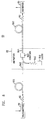
- FIG. 1 An exemplary embodiment 10 of the invention is schematically depicted in FIG. 1.
- Numeral 11 refers to the semiconductor substrate (exemplarily n+ GaAs), 12 to the first cladding layer (exemplarily n InGaP), and 13 to the active layer (comprising one or more strained QW layers).
- numeral 14 refers to the second cladding layer (exemplarily p InGaP), 15 to an optional stop-etch layer (exemplarily p GaAs), 16 to the patterned blocking layer (exemplarily n InGaP), 17 to an optional waveguiding layer (exemplarily p GaAs), 18 to still another cladding layer (exemplarily p InGaP), 19 to a cap layer (exemplarily p+ GaAs), and 20 and 21 to conventional metal contact layers (exemplarily respectively AuBe/Ti/Au and Au/Sn/Au).
- FIG. 1 does not necessarily show every layer that may desirably be incorporated into an actual device. Instead, FIG. 1 shows those features that are required to understand the operative principle of the exemplary embodiment.
- FIGs. 3 and 2 show in conventional form the conduction band edges associated with the exemplary embodiment of FIG. 1, along lines AA' and BB', respectively.
- Numeral 28 refers to the conduction band edge of cladding 18, 27 to that of waveguide layer 17, 26 to that of blocking layer 16, 25 to that of stop-etch layer 15, and 24 to that of cladding layer 14.
- numerals 231 and 233 refer to the conduction band edge of the barrier layers, and 232 to that of the QW sandwiched between the barrier layers.
- Numeral 29 refers to the lowest bound energy level associated with the QW. For simplicity's sake only one QW is shown.
- numeral 22 refers to the conduction band edge of cladding layer 12. The corresponding valence band edges are not shown but can be readily drawn for any appropriate combination of materials.
- the exemplary embodiment of FIG. 1 comprises a blocking layer 16 whose bandgap energy E g is greater than that associated with the active region. Furthermore, since E g of the blocking layer 16 is less than or equal to E g of cladding layer 18 (and therefore in general the refractive index of 16 is greater than or equal to that of 18), lateral waveguiding is provided by waveguide layer 17.
- the composition of the blocking layer 16 such that the blocking layer material has E g greater than that of cladding layer 18 (and consequently the refractive index of 16 is less than that of 18).
- waveguide layer 17 is optional, since such a structure would exhibit lateral guiding even without the waveguide layer.
- a further embodiment 40 of the invention is schematically depicted in FIG. 4.
- the blocking layer comprises a multiplicity of QWs.
- the instnat embodiment of the invention involves lateral radiation confinement through absorption.
- the relative amount of absorption depends on, e.g., the distance between 43 and 46, and the number and thickness of blocking layer QWs.
- the thickness of blocking layer 46 is at least 0.1 ⁇ m, since a significantly thinner blocking layer may be subject to electrical break-down or excessive leakage.
- the thicknesses of all the QWs of course are selected such that they are below the respective (known) critical thicknesses, in order to insure a dislocation-free structure.
- a laser substantially as shown by FIG. 1 was made as follows. On a (100)n+ GaAs wafer was grown in sequence by gas source MBE a 0.2 ⁇ m buffer layer consisting of a lattice matched superlattice (10 pairs n+ InGaP/GaAs; each layer being 10 nm thick), a 1.5 ⁇ m n+ InGaP cladding layer, a 0.1 ⁇ m GaAs separate confinement heterostructure (SCH) layer, three 7 nm In 0.2 Ga 0.8 As strained QW layers separated by 20 nm GaAs barrier layers, a 0.1 ⁇ m GaAs SCH layer, a 0.1 ⁇ m p+ InGaP barrier layer, a 10 nm p+ GaAs stop-etch layer, and a 0.2 ⁇ m n+ InGaP blocking layer.
- the combination of SCH layer/3 QWs/SCH layer corresponds to active layer 13 in FIG. 1.
- the wafer was patterned with SiO2 window stripes of various widths, aligned along the ⁇ 1 1 ⁇ 0> crystal direction to provide positive slopes after etching.
- Channels were delineated by removing the elongate exposed portions of the n+ InGaP blocking layer by selective wet chemical etching with 3:1 HCl/H2O.
- the SiO2 etch mask and the exposed portions of the n+ GaAs stop-etch layer were removed by conventional means, and the wafer was re-loaded into the growth chamber for the second growth sequence.
- the second growth consisted of GSMBE growth of a 0.1 ⁇ m p+ GaAs waveguide layer, a 1.0 ⁇ m p+ InGaP cladding layer, and a 0.2 ⁇ m p+ GaAs cap layer. Unless otherwise noted, all InGaP layers had the In 0.49 Ga 0.51 P lattice matched composition. Growth was at 520°C, n-type material was doped with Si, and p-type material with Be.
- the wafer was thinned to about 0.1 mm and conventionally alloyed with AuBe/Ti/Au and Au/Sn/Au as p- and n-type metal contact layers, respectively. Then the wafer was cleaved into bodies of approximate dimensions 0.5 mm by 0.5 mm, the facets were coated in conventional manner, and the thus produced lasers were mounted, junction side up, on Cu heat sinks. Any processing steps not explicitly recited were conventional and well known.
- FIG. 5 shows exemplary CW room temperature data, for AR/HR coated lasers (produced as described above) with, respectively, 2.5 and 4.5 ⁇ m wide openings in the blocking layer.
- the lasers exhibited threshold currents of 12 and 14 mA, respectively, an external differential quantum efficiency of 0.68 mW/mA, and a peak power emitted into free space of 61 and 83 mW, respectively.
- FIG. 6 shows exemplary data of emission intensity vs. wavelength of a laser, made as described above, with 2.5 ⁇ m blocking layer opening.
- the room temperature CW data was taken at 30 mW output power, and clearly shows that the emission is single mode, centered at 1.005 ⁇ m wavelength, with side mode suppression ratio of more than 30 db. Fundamental mode lasing typically was observed up to the highest output powers.
- Those skilled in the art will appreciate that only minor changes in composition and/or QW thickness would be required to result in a laser whose output is centered at 0.98 ⁇ m.
- FIG. 7 shows exemplary data on output power vs. drive current, for temperatures from 30 to 145°C, for a 2.5 ⁇ m opening width lasers produced as described above.
- the laser exhibited a critical temperature (T o ) of 130K. From measurements on lasers of varying cavity length, an estimated typical internal differential quantum efficiency of about 82% and a typical waveguide loss of about 12 cm ⁇ 1 were obtained.
- a further embodiment has a structure as shown in FIG. 1, except that claddings 12 and 14 are n Al 0.4 Ga 0.6 As, stop-etch layer 15 is p AlAs, and blocking layer 16 and cladding 18 are p Al 0.4 Ga 0.6 As.
- FIG. 8 schematically depicts an exemplary article according to the invention, namely, optical fiber communication system 80 that comprises optical amplifier means 84.
- Modulated radiation 82 e.g., of approximate wavelength 1.55 ⁇ m
- the amplifier 84 comprises a conventional wavelength division multiplexed (WDM) coupler connected, by conventional connection means 843, to a length of Er-doped optical fiber 844.
- WDM wavelength division multiplexed
- Pump radiation 845 of approximate wavelength 0.98 ⁇ m is produced by inventive laser 841 and is coupled into the pump arm of the WDM coupler 842 and co-propagates with the signal radiation in the Er-doped fiber, resulting in amplification of the signal.
- optical fiber communication systems can be bi-directional, and that pump radiation can be co- as well as counter-propagating with the signal radiation.
- a variety of conventional components e.g., means for providing a drive current to pump laser 841) are not shown in FIG. 8.
Landscapes
- Physics & Mathematics (AREA)
- Optics & Photonics (AREA)
- Nanotechnology (AREA)
- Engineering & Computer Science (AREA)
- Chemical & Material Sciences (AREA)
- General Physics & Mathematics (AREA)
- Life Sciences & Earth Sciences (AREA)
- Biophysics (AREA)
- Electromagnetism (AREA)
- Condensed Matter Physics & Semiconductors (AREA)
- Crystallography & Structural Chemistry (AREA)
- Geometry (AREA)
- Semiconductor Lasers (AREA)
- Lasers (AREA)
Applications Claiming Priority (2)
| Application Number | Priority Date | Filing Date | Title |
|---|---|---|---|
| US07/800,772 US5212704A (en) | 1991-11-27 | 1991-11-27 | Article comprising a strained layer quantum well laser |
| US800772 | 2001-03-07 |
Publications (2)
| Publication Number | Publication Date |
|---|---|
| EP0544439A1 true EP0544439A1 (de) | 1993-06-02 |
| EP0544439B1 EP0544439B1 (de) | 1996-01-31 |
Family
ID=25179316
Family Applications (1)
| Application Number | Title | Priority Date | Filing Date |
|---|---|---|---|
| EP92310489A Expired - Lifetime EP0544439B1 (de) | 1991-11-27 | 1992-11-18 | Gegenstand mit einem spannungsverformten Quantumwell-Laser |
Country Status (4)
| Country | Link |
|---|---|
| US (1) | US5212704A (de) |
| EP (1) | EP0544439B1 (de) |
| JP (1) | JPH05226789A (de) |
| DE (1) | DE69208055T2 (de) |
Cited By (5)
| Publication number | Priority date | Publication date | Assignee | Title |
|---|---|---|---|---|
| EP0666625A1 (de) * | 1994-01-31 | 1995-08-09 | Mitsubishi Chemical Corporation | Verfahren zur Herstellung einer Nut in einem Halbleiterlaser und einer Halbleiterlaser |
| GB2301481A (en) * | 1995-04-06 | 1996-12-04 | Mitsubishi Electric Corp | Semiconductor laser |
| EP1104057A3 (de) * | 1999-11-19 | 2003-11-26 | Fuji Photo Film Co., Ltd. | Hochleistungshalbleiterlaser mit Strombegrenzung und indexgeführter Struktur |
| WO2004001918A3 (en) * | 2002-06-22 | 2004-06-17 | Bookham Technology Plc | An index-guided self-aligned laser structure with current blocking layer |
| US20170373473A1 (en) * | 2014-12-03 | 2017-12-28 | Alpes Lasers Sa | Quantum cascade laser with current blocking layers |
Families Citing this family (13)
| Publication number | Priority date | Publication date | Assignee | Title |
|---|---|---|---|---|
| US5471494A (en) * | 1992-04-08 | 1995-11-28 | Rohm Co., Ltd. | Method for selecting a self pulsating semiconductor laser |
| KR950008863B1 (ko) * | 1992-04-13 | 1995-08-08 | 주식회사금성사 | 반도체 레이저 다이오드 |
| KR950004667A (ko) * | 1993-07-29 | 1995-02-18 | 가나이 쯔또무 | 반도체레이저소자 및 그 제작방법 |
| JPH08222815A (ja) * | 1994-12-13 | 1996-08-30 | Mitsubishi Electric Corp | 半導体レーザ装置の製造方法、及び半導体レーザ装置 |
| US5663976A (en) * | 1995-10-16 | 1997-09-02 | Northwestern University | Buried-ridge laser device |
| US5760939A (en) * | 1995-10-23 | 1998-06-02 | Sdl, Inc. | Optical transmission link capable of high temperature operation without cooling with an optical receiver module having temperature independent sensitivity performance and optical transmitter module with laser diode source |
| US5832017A (en) * | 1996-03-15 | 1998-11-03 | Motorola Inc | Reliable near IR VCSEL |
| US6330263B1 (en) * | 1998-05-06 | 2001-12-11 | Sarnoff Corporation | Laser diode having separated, highly-strained quantum wells |
| US6087207A (en) * | 1998-09-29 | 2000-07-11 | Raytheon Company | Method of making pseudomorphic high electron mobility transistors |
| JP2001068789A (ja) * | 1999-08-26 | 2001-03-16 | Fuji Photo Film Co Ltd | 半導体レーザ |
| US20020090167A1 (en) * | 2001-01-08 | 2002-07-11 | Michael Geva | Electronic device having a barrier region including aluminum and a method of manufacture therefor |
| US6574260B2 (en) | 2001-03-15 | 2003-06-03 | Corning Lasertron Incorporated | Electroabsorption modulated laser |
| JP2008283096A (ja) * | 2007-05-14 | 2008-11-20 | Hitachi Cable Ltd | 半導体発光素子 |
Citations (2)
| Publication number | Priority date | Publication date | Assignee | Title |
|---|---|---|---|---|
| EP0426419A2 (de) * | 1989-10-31 | 1991-05-08 | The Furukawa Electric Co., Ltd. | Halbleiterlaser-Elemente und Verfahren zu ihrer Herstellung |
| EP0444366A2 (de) * | 1990-02-28 | 1991-09-04 | Kabushiki Kaisha Toshiba | Halbleiterlaser mit Grabenprofil in Form einer inversen Mesa |
Family Cites Families (1)
| Publication number | Priority date | Publication date | Assignee | Title |
|---|---|---|---|---|
| US4881235A (en) * | 1985-07-26 | 1989-11-14 | Hitachi, Ltd. | Semiconductor laser having a multiple quantum well structure doped with impurities |
-
1991
- 1991-11-27 US US07/800,772 patent/US5212704A/en not_active Expired - Lifetime
-
1992
- 1992-11-18 EP EP92310489A patent/EP0544439B1/de not_active Expired - Lifetime
- 1992-11-18 DE DE69208055T patent/DE69208055T2/de not_active Expired - Fee Related
- 1992-11-27 JP JP4318049A patent/JPH05226789A/ja active Pending
Patent Citations (2)
| Publication number | Priority date | Publication date | Assignee | Title |
|---|---|---|---|---|
| EP0426419A2 (de) * | 1989-10-31 | 1991-05-08 | The Furukawa Electric Co., Ltd. | Halbleiterlaser-Elemente und Verfahren zu ihrer Herstellung |
| EP0444366A2 (de) * | 1990-02-28 | 1991-09-04 | Kabushiki Kaisha Toshiba | Halbleiterlaser mit Grabenprofil in Form einer inversen Mesa |
Non-Patent Citations (7)
| Title |
|---|
| APPLIED PHYSICS LETTERS. vol. 45, no. 8, 15 October 1984, NEW YORK US pages 818 - 820 K. UOMI ET AL. 'High-power operation of index-guided visible GaAs/GaAlAs multiquantum well lasers' * |
| APPLIED PHYSICS LETTERS. vol. 55, no. 21, 20 November 1989, NEW YORK US pages 2167 - 2169 K.J. BEERNINK ET AL. 'Characterization of InGaAs-GaAs strained-layer lasers with quantum wells near the critical thickness' * |
| APPLIED PHYSICS LETTERS. vol. 56, no. 19, 7 May 1990, NEW YORK US pages 1828 - 1830 J.E. EPLER ET AL. 'Current confinement in a GaAs/AlGaAs heterostructure by In Situ laserpatterned desorption of a current-blocking quantum well' * |
| APPLIED PHYSICS LETTERS. vol. 59, no. 22, 25 November 1991, NEW YORK US pages 2781 - 2783 J.M. KUO ET AL. 'InGaAs/GaAs/InGaP multiple-quantum-well lasers prepared by gas-source molecular beam epitaxy' * |
| APPLIED PHYSICS LETTERS. vol. 59, no. 23, 2 December 1991, NEW YORK US pages 2929 - 2931 Y.K. CHEN ET AL. 'Self-aligned InGaAs/GaAs/InGaP quantum well lasers prepared by gas-source molecular beam epitaxy with two growth steps' * |
| IEEE PHOTONICS TECHNOLOGY LETTERS vol. 3, no. 7, July 1991, NEW YORK US pages 585 - 587 C.P. CHAO ET AL. 'Fabrication of low-threshold InGaAs/GaAs ridge waveguide lasers by using In Situ monitored reactive ion etching' * |
| PATENT ABSTRACTS OF JAPAN vol. 14, no. 108 (E-896)27 February 1990 & JP-A-01 309 391 ( OKI ELECTRIC IND. CO. LTD. ) * |
Cited By (9)
| Publication number | Priority date | Publication date | Assignee | Title |
|---|---|---|---|---|
| EP0666625A1 (de) * | 1994-01-31 | 1995-08-09 | Mitsubishi Chemical Corporation | Verfahren zur Herstellung einer Nut in einem Halbleiterlaser und einer Halbleiterlaser |
| US5566198A (en) * | 1994-01-31 | 1996-10-15 | Mitsubishi Chemical Corporation | Method of forming a groove in a semiconductor laser diode and a semiconductor laser diode |
| US5920767A (en) * | 1994-01-31 | 1999-07-06 | Mitsubishi Chemical Company | Method of forming a groove in a semiconductor laser diode and a semiconductor laser diode |
| GB2301481A (en) * | 1995-04-06 | 1996-12-04 | Mitsubishi Electric Corp | Semiconductor laser |
| GB2301481B (en) * | 1995-04-06 | 1997-10-08 | Mitsubishi Electric Corp | Semiconductor laser device and fabricating method thereof |
| EP1104057A3 (de) * | 1999-11-19 | 2003-11-26 | Fuji Photo Film Co., Ltd. | Hochleistungshalbleiterlaser mit Strombegrenzung und indexgeführter Struktur |
| WO2004001918A3 (en) * | 2002-06-22 | 2004-06-17 | Bookham Technology Plc | An index-guided self-aligned laser structure with current blocking layer |
| US20170373473A1 (en) * | 2014-12-03 | 2017-12-28 | Alpes Lasers Sa | Quantum cascade laser with current blocking layers |
| US10374393B2 (en) * | 2014-12-03 | 2019-08-06 | Alpes Lasers Sa | Quantum cascade laser with current blocking layers |
Also Published As
| Publication number | Publication date |
|---|---|
| DE69208055D1 (de) | 1996-03-14 |
| DE69208055T2 (de) | 1996-09-05 |
| EP0544439B1 (de) | 1996-01-31 |
| US5212704A (en) | 1993-05-18 |
| JPH05226789A (ja) | 1993-09-03 |
Similar Documents
| Publication | Publication Date | Title |
|---|---|---|
| EP0544439B1 (de) | Gegenstand mit einem spannungsverformten Quantumwell-Laser | |
| US5381434A (en) | High-temperature, uncooled diode laser | |
| US5208821A (en) | Buried heterostructure lasers using MOCVD growth over patterned substrates | |
| EP0661782B1 (de) | Halbleiterlaser | |
| EP0132081B1 (de) | Halbleiterlaser | |
| US5289484A (en) | Laser diode | |
| US5260959A (en) | Narrow beam divergence laser diode | |
| JPH0381317B2 (de) | ||
| US6472691B2 (en) | Distributed feedback semiconductor laser device | |
| EP0503211A1 (de) | Halbleiteranordnung mit einer auf einem strukturierten Substrat aufgewachsenen Schichtstruktur | |
| Ishikawa et al. | 0.98-1.02 mu m strained InGaAs/AlGaAs double quantum-well high-power lasers with GaInP buried waveguides | |
| EP0843393B1 (de) | Halbleiterdiodenlaser | |
| US5572616A (en) | Waveguide device | |
| US5852625A (en) | Distributed feedback semiconductor laser | |
| US5309465A (en) | Ridge waveguide semiconductor laser with thin active region | |
| JP3242958B2 (ja) | 光半導体素子 | |
| JP3488137B2 (ja) | 光半導体装置およびその製造方法 | |
| US5136601A (en) | Semiconductor laser | |
| US4890292A (en) | Semiconductor laser device | |
| US20050008053A1 (en) | Complex coupled single mode laser with dual active region | |
| EP0525971B1 (de) | Halbleitervorrichtung und Verfahren zur Herstellung derselben | |
| JP4163343B2 (ja) | 発光素子および発光素子モジュール | |
| EP1085626A1 (de) | Halbleiterlaser | |
| JP3040262B2 (ja) | 半導体レーザ装置 | |
| Gignac et al. | High power InGaAs/AlGaAs singlemode laser diodes suitable for pumping Pr3+-doped fluoride fibre optic amplifiers |
Legal Events
| Date | Code | Title | Description |
|---|---|---|---|
| PUAI | Public reference made under article 153(3) epc to a published international application that has entered the european phase |
Free format text: ORIGINAL CODE: 0009012 |
|
| AK | Designated contracting states |
Kind code of ref document: A1 Designated state(s): DE FR GB |
|
| 17P | Request for examination filed |
Effective date: 19931118 |
|
| RAP3 | Party data changed (applicant data changed or rights of an application transferred) |
Owner name: AT&T CORP. |
|
| 17Q | First examination report despatched |
Effective date: 19940603 |
|
| GRAA | (expected) grant |
Free format text: ORIGINAL CODE: 0009210 |
|
| AK | Designated contracting states |
Kind code of ref document: B1 Designated state(s): DE FR GB |
|
| REF | Corresponds to: |
Ref document number: 69208055 Country of ref document: DE Date of ref document: 19960314 |
|
| ET | Fr: translation filed | ||
| PLBE | No opposition filed within time limit |
Free format text: ORIGINAL CODE: 0009261 |
|
| 26N | No opposition filed | ||
| PGFP | Annual fee paid to national office [announced via postgrant information from national office to epo] |
Ref country code: FR Payment date: 20011022 Year of fee payment: 10 |
|
| PGFP | Annual fee paid to national office [announced via postgrant information from national office to epo] |
Ref country code: DE Payment date: 20011230 Year of fee payment: 10 |
|
| REG | Reference to a national code |
Ref country code: GB Ref legal event code: IF02 |
|
| PG25 | Lapsed in a contracting state [announced via postgrant information from national office to epo] |
Ref country code: DE Free format text: LAPSE BECAUSE OF NON-PAYMENT OF DUE FEES Effective date: 20030603 |
|
| PG25 | Lapsed in a contracting state [announced via postgrant information from national office to epo] |
Ref country code: FR Free format text: LAPSE BECAUSE OF NON-PAYMENT OF DUE FEES Effective date: 20030731 |
|
| REG | Reference to a national code |
Ref country code: FR Ref legal event code: ST |
|
| PGFP | Annual fee paid to national office [announced via postgrant information from national office to epo] |
Ref country code: GB Payment date: 20101118 Year of fee payment: 19 |
|
| REG | Reference to a national code |
Ref country code: GB Ref legal event code: PE20 Expiry date: 20121117 |
|
| PG25 | Lapsed in a contracting state [announced via postgrant information from national office to epo] |
Ref country code: GB Free format text: LAPSE BECAUSE OF EXPIRATION OF PROTECTION Effective date: 20121117 |