EP0564895A1 - Ballast électronique pour lampes à décharge basse-pression - Google Patents
Ballast électronique pour lampes à décharge basse-pression Download PDFInfo
- Publication number
- EP0564895A1 EP0564895A1 EP93104806A EP93104806A EP0564895A1 EP 0564895 A1 EP0564895 A1 EP 0564895A1 EP 93104806 A EP93104806 A EP 93104806A EP 93104806 A EP93104806 A EP 93104806A EP 0564895 A1 EP0564895 A1 EP 0564895A1
- Authority
- EP
- European Patent Office
- Prior art keywords
- voltage
- capacitor
- discharge lamp
- diode
- circuit
- Prior art date
- Legal status (The legal status is an assumption and is not a legal conclusion. Google has not performed a legal analysis and makes no representation as to the accuracy of the status listed.)
- Granted
Links
Images

Classifications
-
- H—ELECTRICITY
- H05—ELECTRIC TECHNIQUES NOT OTHERWISE PROVIDED FOR
- H05B—ELECTRIC HEATING; ELECTRIC LIGHT SOURCES NOT OTHERWISE PROVIDED FOR; CIRCUIT ARRANGEMENTS FOR ELECTRIC LIGHT SOURCES, IN GENERAL
- H05B41/00—Circuit arrangements or apparatus for igniting or operating discharge lamps
- H05B41/14—Circuit arrangements
- H05B41/26—Circuit arrangements in which the lamp is fed by power derived from DC by means of a converter, e.g. by high-voltage DC
- H05B41/28—Circuit arrangements in which the lamp is fed by power derived from DC by means of a converter, e.g. by high-voltage DC using static converters
- H05B41/295—Circuit arrangements in which the lamp is fed by power derived from DC by means of a converter, e.g. by high-voltage DC using static converters with semiconductor devices and specially adapted for lamps with preheating electrodes, e.g. for fluorescent lamps
- H05B41/298—Arrangements for protecting lamps or circuits against abnormal operating conditions
- H05B41/2981—Arrangements for protecting lamps or circuits against abnormal operating conditions for protecting the circuit against abnormal operating conditions
- H05B41/2985—Arrangements for protecting lamps or circuits against abnormal operating conditions for protecting the circuit against abnormal operating conditions against abnormal lamp operating conditions
-
- H—ELECTRICITY
- H02—GENERATION; CONVERSION OR DISTRIBUTION OF ELECTRIC POWER
- H02M—APPARATUS FOR CONVERSION BETWEEN AC AND AC, BETWEEN AC AND DC, OR BETWEEN DC AND DC, AND FOR USE WITH MAINS OR SIMILAR POWER SUPPLY SYSTEMS; CONVERSION OF DC OR AC INPUT POWER INTO SURGE OUTPUT POWER; CONTROL OR REGULATION THEREOF
- H02M1/00—Details of apparatus for conversion
- H02M1/0003—Details of control, feedback or regulation circuits
- H02M1/0006—Arrangements for supplying an adequate voltage to the control circuit of converters
Definitions
- the present invention relates to an electronic ballast for a low-pressure gas discharge lamp according to the preamble of patent claim 1.
- the latter device contains an electronic harmonic filter designed as a step-up converter, the electronic harmonic filter having a step-up choke.
- the step-up converter choke has an additional auxiliary winding which, when the ballast is switched on, continuously charges a capacitor via a rectifier circuit, which supplies the control circuit with a DC supply voltage.
- a Zener diode is connected in parallel to the capacitor.
- This known DC voltage supply circuit for the control circuit of the inverter has the main disadvantage that it requires a continuous and noticeable current flow through several semiconductor elements and resistors to generate the DC supply voltage, regardless of the proportion of the energy required in the control circuit is what leads to undesirable losses and additional warming.
- the control circuit and thus the inverter can also be in the operating state when the discharge lamp is defective or is not present at all, which can lead to damage due to the overvoltages that arise.
- the object of the present invention is to provide an electronic ballast of the type mentioned, the DC voltage supply circuit for the control circuit is only effective in accordance with the required electrical energy and only when a functional discharge lamp is connected to the ballast.
- the electronic ballast according to the invention has the features stated in the characterizing part of patent claim 1.
- the current detection element Since the current detection element is short-circuited by the voltage threshold switch when the charge of the storage capacitor or its voltage is sufficient to maintain the supply voltage for the control circuit, unnecessary losses are kept to a minimum. Furthermore, since the actual current of the discharge circuit is measured by the current detection element, it is ensured that operation of the control circuit and thus of the inverter is prevented in the event of a defect in the discharge circuit, in particular if the discharge lamp is defective or missing.
- the voltage threshold switch can consist essentially of two transistors and a Zener diode.
- an initial supply voltage for the control circuit which is required after the ballast is switched on can be generated with the aid of an electronic switch connected to a rectifier on the mains side.
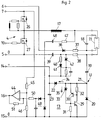
- a bridge rectifier 2 is connected to terminals 1 for an AC or DC network.
- the bridge rectifier forms a full wave; in a DC network, the bridge rectifier serves as reverse polarity protection.
- An electronic step-up converter 3 is connected to the bridge rectifier 2.
- This enables a stepless transformation of the input DC voltage from, for example, 230 V to a higher output DC voltage level of, for example, 400 V.
- the output DC voltage of the step-up converter feeds an only schematically illustrated inverter 4, which is also connected to a common zero line 0, indicated by a terminal 5
- the pulsating DC voltage of the bridge rectifier 2 and the output DC voltage of the step-up converter 3 are supplied to further circuit parts which are only explained in FIG. 2, which is indicated in FIG. 1 by a terminal 6 and a terminal 7, respectively.
- the inverter 4 periodically and alternately switches the DC output voltage of the step-up converter 3 and the zero voltage of the zero line 0 to its output connection.
- An electronic control unit 8 the connection of which to the inverter 4 is indicated by terminals 9 and 10 and is also used with the aid of FIG. 2, is used to control its electronic switching paths is explained in more detail.
- the control circuit 8 controls the inverter 4 with rectangular pulses of a higher frequency of the order of 50 kHz.
- these square-wave pulses can be changed either in terms of pulse width or pulse frequency in the control circuit 8, which can be achieved from the outside by means of a control voltage supplied by means of connecting terminals 12.
- the control circuit 8 requires a DC supply voltage of, for example, 12 V, for which purpose, according to FIG. 1, a DC voltage supply circuit generally designated 13 with indicated connection terminals 14 and 15 is used. As can be seen, the DC voltage supply circuit 13 also feeds electronic circuit parts of the step-up converter 3 via the connection terminals 14, 15.
- a commercially available integrated circuit contained in the control circuit 8 has a switch-off connection, to which reference is made in the more detailed diagram in FIG. 2, and which is indicated in Fig. 1 by a clamp 16.
- the discharge circuit connected to the inverter 4 consists of a choke 17 connected in series with the discharge lamp 11, a capacitor 18 connected in parallel with the discharge lamp 11, and basically another capacitor 19 connected in series with the discharge lamp 11, which is connected to the common zero line 0 stands. Accordingly, the total current of the named discharge circuit flows via the capacitor 19, which is used in the following manner to generate the DC supply voltage for the control circuit 8 and also the step-up converter 3 by means of the DC voltage supply circuit 13.
- the series capacitor 19 is not, as usual, connected directly to the zero line 0, but is connected to it via a series diode 20.
- the diode 20 is arranged such that it is for a negative current is permeable, but blocks a positive current.
- a positive voltage occurs for each positive half cycle of the current in the discharge circuit, which charges a capacitor 23 via a diode 22.
- the diode 22 prevents the capacitor 23 from discharging again when the series diode 20 is conductive during the negative half-periods of the current in the discharge circuit.
- the series diode 20 has an electronic switch 24 connected in parallel.
- the switch 24 is electronically influenced by a control element 25, which is also connected in parallel to the series diode 20, the control element 25 responding in each positive half-period and closing the switch 24 when the positive voltage at the connection point 21 reaches a certain value.
- the switch 24 is closed, the current of the discharge circuit flows directly to the zero line O, so that the capacitor 23 is not further charged.
- the inductor 17 is connected in series with the discharge lamp 11, the capacitor 18 in parallel with the discharge lamp 11, and further in series with the discharge lamp 11 and its capacitor 19, the capacitor 19 and the diode 20th
- the inverter 4 has two MOSFET transistors 26 and 27 as electronic switching elements. While the transistor 27 is controlled directly by the control circuit 8 via the connection 10, the transistor 26 is controlled because of the high voltage level at its source in each half period -Electrode via a transformer, of which the secondary winding 28 is shown in FIG. 2.
- the DC voltage supply circuit 13 has, in parallel to the diode 20, the circuit of an npn transistor 29 and a pnp transistor 30, the collector of one transistor being connected to the base of the other transistor. Furthermore, the bases of both transistors 29, 30 are each connected via a resistor 31, 32 to the zero line 0 or to the line of the connection point 21. Finally, a Zener diode 33 is connected between the line of the connection point 21 and the base of the transistor 29.
- this current flows from the capacitor 19 via the diode 20 directly to the zero line 0. Accordingly, a very low negative voltage is present at the connection point 21, corresponding to the voltage drop across the diode 20.
- FIG. 3 shows the time course of the voltage U in the connection point in accordance with the above statements, the positive and negative half-cycle of the current in the discharge circuit being denoted by + and -.
- the double arrow indicates that the time width of the positive pulse charging the capacitor 23 is variable, that is to say it depends on the respective state of charge of the capacitor 23.
- the described DC voltage supply circuit can only function if a current flows in the discharge circuit, that is to say the discharge lamp is ignited, it is necessary in a manner known per se to provide a first, brief supply voltage supply when the ballast is switched on. The following measures have been taken in this ballast.
- a line is led via a diode 36 and a first resistor 37 to the first heating connection of the second electrode of the discharge lamp 11 in the discharge circuit.
- the line leads from the second heating connection of the lamp electrode via a further resistor 38 to a capacitor 39 which is connected to the zero line 0.
- an electronic switch is connected to this line, which has a thyristor 41 provided with a current limiting resistor 40, a Zener diode 42 connected between the said line and the control electrode of the thyristor 41, and between the control electrode and the cathode of thyristor 41 contains the parallel circuit 43 of a resistor and a capacitor.
- the cathode of the thyristor 41 and the parallel circuit 43 are connected to the feed line + of the DC voltage supply circuit 13.
- the DC voltage now present at terminal 6 charges the capacitor 39 via the resistors 37 and 38.
- the control electrode of the thyristor 41 receives a positive voltage and the thyristor 41 ignites.
- the capacitor 39 discharges via the conductive thyristor 41 onto the capacitor 23, so that a positive voltage appears at the supply terminal 14, which feeds the control circuit 8 and the step-up converter.
- the electronic circuit parts of the control circuit 8 and the step-up converter 3 become active, which leads to the ignition of the discharge lamp 11 and to a normal operating state.
- the capacitor 39 and the zener diode 42 are dimensioned in such a way that the charge on the capacitor is sufficient to supply the control circuit 8 and the step-up converter 3 sufficiently until the discharge lamp 11 is ignited.
- a drop in the voltage at the Zener diode 42 and thus its blocking are irrelevant, since the thyristor, due to its very low holding current, can only extinguish when the supply via the resistor 38 fails, that is to say when the ballast is switched off or the Discharge lamp 11 is removed or suffers a defect.
- a defective or unsatisfactorily burning discharge lamp can therefore be replaced when the ballast is switched on, after the insertion of the new discharge lamp the described initial process of generating the DC supply voltage with the advantage of temporarily automatically switching off the control circuit 8 and the step-up converter 3 and so that the inverter also automatically runs again.
- FIG. 2 shows a further auxiliary circuit of the present ballast, namely a switch-off arrangement when it occurs an overvoltage in the discharge circuit.
- the output of an operational amplifier 44 is connected to the connecting terminal 16 and thus, as already mentioned, to a switch-off connection of the integrated circuit contained in the control circuit 8.
- the negative input - of the operational amplifier 44 is connected to a voltage divider 45, 46, which is arranged between the supply voltage of the inverter 4 (terminal 7) and the zero line 0.
- the positive input + of the operational amplifier 44 is connected to the connection of the choke 17 to the one electrode of the discharge lamp 11, specifically via a first series resistor 47, a capacitor 48, a rectifier circuit 49 and a second series resistor 50.
- the positive input + and the output of the operational amplifier 44 are connected to one another via a resistor 51, which on the one hand acts as a feedback for fast switching of the operational amplifier 44 and on the other hand, as explained below, as a connection for the voltage divider formed by the resistors 47, 50.
- the voltage dividers 45, 46 and 47, 50, 51 are dimensioned such that, in the normal operating state of the ballast, the voltage at the negative input - of the operational amplifier 44 is higher than at the positive input +. Then the output of the operational amplifier 44 is practically at the zero potential of the zero line 0, which, as mentioned, defines the voltage divider 47, 50, 51. At the terminal 16 and thus at the shutdown connection of the integrated circuit of the control circuit 8 there is also the zero potential, which does not affect the integrated circuit, that is to say leaves it effective.
- the switch-off arrangement described is effective in the same way if the supply voltage of the inverter 4 (terminal 7) drops without the voltage after the inductor 17 falling accordingly. Such an accident is likely to be rare, but could be caused by an abnormal operating condition. Even then, the voltage at the negative input - of the operational amplifier 44 is lower than that at the positive input +, so that the control circuit 8 is subsequently switched off.
- a comparator or a transistor circuit can also be used by making appropriate circuit changes.
- the thyristor 41 can also be replaced by a transistor circuit with the same functions.
- a suggested replacement of the two transistors 29, 30 by a thyristor is not feasible, since this switching element would not erase when the charging voltage for the capacitor 23 determined by the Zener diode 33 was reached.
- the electronic ballast according to the invention accordingly enables safe, effortless and virtually all eventual operation of the discharge lamp with relatively little outlay on components. In addition, electrical losses and thus excessive heat generation are minimized.
Landscapes
- Circuit Arrangements For Discharge Lamps (AREA)
- Discharge Lamp (AREA)
Applications Claiming Priority (2)
| Application Number | Priority Date | Filing Date | Title |
|---|---|---|---|
| CH1117/92A CH683219A5 (de) | 1992-04-06 | 1992-04-06 | Elektronisches Vorschaltgerät für eine Niederdruck-Gasentladungslampe. |
| CH1117/92 | 1992-04-06 |
Publications (2)
| Publication Number | Publication Date |
|---|---|
| EP0564895A1 true EP0564895A1 (fr) | 1993-10-13 |
| EP0564895B1 EP0564895B1 (fr) | 1996-10-09 |
Family
ID=4202890
Family Applications (1)
| Application Number | Title | Priority Date | Filing Date |
|---|---|---|---|
| EP93104806A Expired - Lifetime EP0564895B1 (fr) | 1992-04-06 | 1993-03-24 | Ballast électronique pour lampes à décharge basse-pression |
Country Status (5)
| Country | Link |
|---|---|
| EP (1) | EP0564895B1 (fr) |
| AT (1) | ATE144094T1 (fr) |
| CH (1) | CH683219A5 (fr) |
| DE (1) | DE59304073D1 (fr) |
| DK (1) | DK0564895T3 (fr) |
Cited By (5)
| Publication number | Priority date | Publication date | Assignee | Title |
|---|---|---|---|---|
| EP0727921A3 (fr) * | 1995-02-17 | 1998-05-27 | Patent-Treuhand-Gesellschaft für elektrische Glühlampen mbH | Circuit pour alimenter une lampe à décharge |
| EP1231821A1 (fr) * | 2001-02-09 | 2002-08-14 | Patent-Treuhand-Gesellschaft für elektrische Glühlampen mbH | Ballast pour lampes électriques |
| EP1289347A3 (fr) * | 2001-08-06 | 2004-05-06 | Osram-Sylvania Inc. | Ballast avec circuit de détection rapide d' une lampe défectueuse |
| WO2007072278A1 (fr) * | 2005-12-22 | 2007-06-28 | Koninklijke Philips Electronics N.V. | Alimentation auxiliaire dans un circuit d’excitation de lampe |
| DE102008016754A1 (de) * | 2008-03-31 | 2009-10-01 | Tridonicatco Gmbh & Co. Kg | Niedervoltversorgung in Betriebsgeräten für Leuchtmittel |
Citations (2)
| Publication number | Priority date | Publication date | Assignee | Title |
|---|---|---|---|---|
| WO1990011005A1 (fr) * | 1989-03-10 | 1990-09-20 | Harel Jean Claude | Dispositif electronique de demarrage et d'alimentation pour tubes fluorescents a electrodes prechauffables |
| EP0439240A2 (fr) * | 1990-01-20 | 1991-07-31 | SEMPERLUX GmbH, LICHTTECHNISCHES WERK | Ballast électronique |
-
1992
- 1992-04-06 CH CH1117/92A patent/CH683219A5/de not_active IP Right Cessation
-
1993
- 1993-03-24 DK DK93104806.0T patent/DK0564895T3/da not_active Application Discontinuation
- 1993-03-24 DE DE59304073T patent/DE59304073D1/de not_active Expired - Fee Related
- 1993-03-24 AT AT93104806T patent/ATE144094T1/de active
- 1993-03-24 EP EP93104806A patent/EP0564895B1/fr not_active Expired - Lifetime
Patent Citations (2)
| Publication number | Priority date | Publication date | Assignee | Title |
|---|---|---|---|---|
| WO1990011005A1 (fr) * | 1989-03-10 | 1990-09-20 | Harel Jean Claude | Dispositif electronique de demarrage et d'alimentation pour tubes fluorescents a electrodes prechauffables |
| EP0439240A2 (fr) * | 1990-01-20 | 1991-07-31 | SEMPERLUX GmbH, LICHTTECHNISCHES WERK | Ballast électronique |
Cited By (5)
| Publication number | Priority date | Publication date | Assignee | Title |
|---|---|---|---|---|
| EP0727921A3 (fr) * | 1995-02-17 | 1998-05-27 | Patent-Treuhand-Gesellschaft für elektrische Glühlampen mbH | Circuit pour alimenter une lampe à décharge |
| EP1231821A1 (fr) * | 2001-02-09 | 2002-08-14 | Patent-Treuhand-Gesellschaft für elektrische Glühlampen mbH | Ballast pour lampes électriques |
| EP1289347A3 (fr) * | 2001-08-06 | 2004-05-06 | Osram-Sylvania Inc. | Ballast avec circuit de détection rapide d' une lampe défectueuse |
| WO2007072278A1 (fr) * | 2005-12-22 | 2007-06-28 | Koninklijke Philips Electronics N.V. | Alimentation auxiliaire dans un circuit d’excitation de lampe |
| DE102008016754A1 (de) * | 2008-03-31 | 2009-10-01 | Tridonicatco Gmbh & Co. Kg | Niedervoltversorgung in Betriebsgeräten für Leuchtmittel |
Also Published As
| Publication number | Publication date |
|---|---|
| EP0564895B1 (fr) | 1996-10-09 |
| ATE144094T1 (de) | 1996-10-15 |
| DE59304073D1 (de) | 1996-11-14 |
| DK0564895T3 (fr) | 1997-03-10 |
| CH683219A5 (de) | 1994-01-31 |
Similar Documents
| Publication | Publication Date | Title |
|---|---|---|
| EP0062275B1 (fr) | Ballast pour le fonctionnement de lampes à décharge à basse pression | |
| EP0306086B1 (fr) | Dispositif de circuit pour le fonctionnement de lampe de décharge à gaz sous haute pression | |
| DE4002334A1 (de) | Lampen-beleuchtungsschaltkreis mit ueberlastschutz | |
| EP0111929A1 (fr) | Dispositif pour la mise hors circuit d'un onduleur | |
| DE2903224A1 (de) | Schaltungsanordnung zum zuenden und speisen einer mit einer vorheizbaren elektrode versehenen metalldampfentladungslampe | |
| DE4120649A1 (de) | Ueberspannungsgeschuetztes vorschaltgeraet | |
| DE3829388A1 (de) | Schaltungsanordnung zum betrieb einer last | |
| EP0146683B1 (fr) | Onduleur | |
| DE2835044A1 (de) | Lastschaltung fuer leuchtstofflampen | |
| EP0614052A2 (fr) | Appareil automatique d'allumage | |
| DE69709652T2 (de) | Universeller elektronischer starter für starkstromentladungslampen | |
| DE3301632A1 (de) | Umrichter | |
| EP0564895B1 (fr) | Ballast électronique pour lampes à décharge basse-pression | |
| WO1979000615A1 (fr) | Installation electronique pour le reglage de l'intensite lumineuse d'une lampe electrique a decharge gazeuse sans cathode incandescente | |
| DE69616451T2 (de) | Umschaltanordnung | |
| EP0389847B1 (fr) | Circuit | |
| DE3530638A1 (de) | Schaltungsanordnung zum starten und betrieb von gasentladungslampen | |
| EP0111956B1 (fr) | Disposition de circuit pour mettre en marche des lampes à décharge à haute pression | |
| EP0055995B1 (fr) | Disposition de circuit d'allumage et fonctionnement d'une lampe de décharge à basse pression à partir d'une source de courant continu | |
| EP0050131B1 (fr) | Ballast pour une lampe a decharge | |
| DE3626209A1 (de) | Vorschaltgeraet fuer wenigstens eine entladungslampe | |
| EP0642295A1 (fr) | Ballast électronique pour alimenter une charge, par exemple une lampe à décharge | |
| EP0120258B1 (fr) | Circuit économiseur d'énergie | |
| EP0021508A1 (fr) | Circuit d'allumage et de commande pour lampes à décharge dans un gaz et/ou une vapeur | |
| EP0069967A1 (fr) | Dispositif pour allumer des lampes fluorescentes |
Legal Events
| Date | Code | Title | Description |
|---|---|---|---|
| PUAI | Public reference made under article 153(3) epc to a published international application that has entered the european phase |
Free format text: ORIGINAL CODE: 0009012 |
|
| AK | Designated contracting states |
Kind code of ref document: A1 Designated state(s): AT BE DE DK FR GB IT NL SE |
|
| 17P | Request for examination filed |
Effective date: 19931218 |
|
| GRAG | Despatch of communication of intention to grant |
Free format text: ORIGINAL CODE: EPIDOS AGRA |
|
| 17Q | First examination report despatched |
Effective date: 19951215 |
|
| GRAH | Despatch of communication of intention to grant a patent |
Free format text: ORIGINAL CODE: EPIDOS IGRA |
|
| GRAH | Despatch of communication of intention to grant a patent |
Free format text: ORIGINAL CODE: EPIDOS IGRA |
|
| GRAA | (expected) grant |
Free format text: ORIGINAL CODE: 0009210 |
|
| AK | Designated contracting states |
Kind code of ref document: B1 Designated state(s): AT BE DE DK FR GB IT NL SE |
|
| REF | Corresponds to: |
Ref document number: 144094 Country of ref document: AT Date of ref document: 19961015 Kind code of ref document: T |
|
| ITF | It: translation for a ep patent filed | ||
| REF | Corresponds to: |
Ref document number: 59304073 Country of ref document: DE Date of ref document: 19961114 |
|
| ET | Fr: translation filed | ||
| GBT | Gb: translation of ep patent filed (gb section 77(6)(a)/1977) |
Effective date: 19961209 |
|
| REG | Reference to a national code |
Ref country code: DK Ref legal event code: T3 |
|
| PLAV | Examination of admissibility of opposition |
Free format text: ORIGINAL CODE: EPIDOS OPEX |
|
| PLBI | Opposition filed |
Free format text: ORIGINAL CODE: 0009260 |
|
| PLBF | Reply of patent proprietor to notice(s) of opposition |
Free format text: ORIGINAL CODE: EPIDOS OBSO |
|
| 26 | Opposition filed |
Opponent name: SIEMENS AG Effective date: 19970704 |
|
| NLR1 | Nl: opposition has been filed with the epo |
Opponent name: SIEMENS AG |
|
| PLBF | Reply of patent proprietor to notice(s) of opposition |
Free format text: ORIGINAL CODE: EPIDOS OBSO |
|
| PLBO | Opposition rejected |
Free format text: ORIGINAL CODE: EPIDOS REJO |
|
| PLBN | Opposition rejected |
Free format text: ORIGINAL CODE: 0009273 |
|
| 27O | Opposition rejected |
Effective date: 19990408 |
|
| PGFP | Annual fee paid to national office [announced via postgrant information from national office to epo] |
Ref country code: DK Payment date: 20000211 Year of fee payment: 8 |
|
| PGFP | Annual fee paid to national office [announced via postgrant information from national office to epo] |
Ref country code: AT Payment date: 20000214 Year of fee payment: 8 Ref country code: FR Payment date: 20000214 Year of fee payment: 8 |
|
| PGFP | Annual fee paid to national office [announced via postgrant information from national office to epo] |
Ref country code: SE Payment date: 20000221 Year of fee payment: 8 |
|
| PGFP | Annual fee paid to national office [announced via postgrant information from national office to epo] |
Ref country code: GB Payment date: 20000222 Year of fee payment: 8 |
|
| PGFP | Annual fee paid to national office [announced via postgrant information from national office to epo] |
Ref country code: DE Payment date: 20000228 Year of fee payment: 8 |
|
| PGFP | Annual fee paid to national office [announced via postgrant information from national office to epo] |
Ref country code: BE Payment date: 20000313 Year of fee payment: 8 |
|
| PGFP | Annual fee paid to national office [announced via postgrant information from national office to epo] |
Ref country code: NL Payment date: 20000331 Year of fee payment: 8 |
|
| PG25 | Lapsed in a contracting state [announced via postgrant information from national office to epo] |
Ref country code: GB Free format text: LAPSE BECAUSE OF NON-PAYMENT OF DUE FEES Effective date: 20010324 Ref country code: DK Free format text: LAPSE BECAUSE OF NON-PAYMENT OF DUE FEES Effective date: 20010324 Ref country code: AT Free format text: LAPSE BECAUSE OF NON-PAYMENT OF DUE FEES Effective date: 20010324 |
|
| PG25 | Lapsed in a contracting state [announced via postgrant information from national office to epo] |
Ref country code: SE Free format text: LAPSE BECAUSE OF NON-PAYMENT OF DUE FEES Effective date: 20010325 |
|
| PG25 | Lapsed in a contracting state [announced via postgrant information from national office to epo] |
Ref country code: BE Free format text: LAPSE BECAUSE OF NON-PAYMENT OF DUE FEES Effective date: 20010331 |
|
| BERE | Be: lapsed |
Owner name: STARKSTROM-ELEKTRONIK A.G. Effective date: 20010331 |
|
| PG25 | Lapsed in a contracting state [announced via postgrant information from national office to epo] |
Ref country code: NL Free format text: LAPSE BECAUSE OF NON-PAYMENT OF DUE FEES Effective date: 20011001 |
|
| EUG | Se: european patent has lapsed |
Ref document number: 93104806.0 |
|
| GBPC | Gb: european patent ceased through non-payment of renewal fee |
Effective date: 20010324 |
|
| REG | Reference to a national code |
Ref country code: DK Ref legal event code: EBP |
|
| PG25 | Lapsed in a contracting state [announced via postgrant information from national office to epo] |
Ref country code: FR Free format text: LAPSE BECAUSE OF NON-PAYMENT OF DUE FEES Effective date: 20011130 |
|
| NLV4 | Nl: lapsed or anulled due to non-payment of the annual fee |
Effective date: 20011001 |
|
| REG | Reference to a national code |
Ref country code: FR Ref legal event code: ST |
|
| PG25 | Lapsed in a contracting state [announced via postgrant information from national office to epo] |
Ref country code: DE Free format text: LAPSE BECAUSE OF NON-PAYMENT OF DUE FEES Effective date: 20020101 |
|
| PG25 | Lapsed in a contracting state [announced via postgrant information from national office to epo] |
Ref country code: IT Free format text: LAPSE BECAUSE OF NON-PAYMENT OF DUE FEES Effective date: 20050324 |