EP0569993A1 - Optical-interference-type angular rate sensor - Google Patents
Optical-interference-type angular rate sensor Download PDFInfo
- Publication number
- EP0569993A1 EP0569993A1 EP93107836A EP93107836A EP0569993A1 EP 0569993 A1 EP0569993 A1 EP 0569993A1 EP 93107836 A EP93107836 A EP 93107836A EP 93107836 A EP93107836 A EP 93107836A EP 0569993 A1 EP0569993 A1 EP 0569993A1
- Authority
- EP
- European Patent Office
- Prior art keywords
- signal
- output
- component
- cosine
- light source
- Prior art date
- Legal status (The legal status is an assumption and is not a legal conclusion. Google has not performed a legal analysis and makes no representation as to the accuracy of the status listed.)
- Granted
Links
Images


Classifications
-
- G—PHYSICS
- G01—MEASURING; TESTING
- G01C—MEASURING DISTANCES, LEVELS OR BEARINGS; SURVEYING; NAVIGATION; GYROSCOPIC INSTRUMENTS; PHOTOGRAMMETRY OR VIDEOGRAMMETRY
- G01C19/00—Gyroscopes; Turn-sensitive devices using vibrating masses; Turn-sensitive devices without moving masses; Measuring angular rate using gyroscopic effects
- G01C19/58—Turn-sensitive devices without moving masses
- G01C19/64—Gyrometers using the Sagnac effect, i.e. rotation-induced shifts between counter-rotating electromagnetic beams
- G01C19/72—Gyrometers using the Sagnac effect, i.e. rotation-induced shifts between counter-rotating electromagnetic beams with counter-rotating light beams in a passive ring, e.g. fibre laser gyrometers
- G01C19/721—Details, e.g. optical or electronical details
Definitions
- the present invention relates to an optical-interference-type angular rate sensor wherein clockwise and counterclockwise light beams (hereinafter referred to as CW and CCW light beams) are passed through an optical path forming at least one loop and the phase difference between the CW and CCW light beams is detected to thereby measure an angular rate applied to the optical path about the axis thereof.
- CW and CCW light beams clockwise and counterclockwise light beams
- ⁇ s 4 ⁇ RL ⁇ /C ⁇ (1)
- C the velocity of light
- ⁇ the wavelength of light in a vacuum
- R the radius of the optical fiber coil 15
- L the length of the optical fiber of the optical fiber coil 15.
- the output Vp of the photodetector 17 is applied to a synchronous detector 18, wherein the same frequency component as the phase modulation frequency f m , that is, the fundamental harmonic component in Eq. (2), is synchronously detected by the reference signal Sr of the same frequency from the reference signal generator 24.
- the detected output is applied to a low-pass filter 19, wherein its AC component is cut off, and the DC level corresponding to the fundamental harmonic component (i.e. the component of the frequency f m ) in Eq. (2) is taken out with a proper gain, as the output of the fiber optic gyro (hereinafter referred to as an FOG output) at an output terminal 21.
- the FOG output V1 is expressed by the following equation: where K A1 is the total gain of the synchronous detector 18 and the low-pass filter 19.
- the input angular rate ⁇ can be detected by measuring the output V1 of the low-pass filter 19.
- a signal corresponding to the phase difference ⁇ s could be detected as the FOG output by the synchronous detection of an arbitrary one of the frequency components in Eq. (2), but it is customary in the art to detect the sin ⁇ s component (an odd harmonic component or simply called sine component) which can be detected with the highest sensitivity when the phase difference ⁇ s is around zero.
- the detected output of such an arbitrary odd harmonic component can be expressed by changing the suffixed numerals in Eq. (4) to a value representing the selected odd harmonic.
- the synchronously detected output V1 of the fiber optic gyro corresponding to the odd harmonic component is a sine function using the phase difference ⁇ s as a variable, as is evident from Eq. (4) and, therefore, if the phase difference ⁇ s is sufficiently small, it can be regarded approximately to be equal to the sin ⁇ s component.
- the FOG output V1 given by Eq. (4) exhibits an excellent linearity with respect to the phase difference ⁇ s , but an increase in the phase difference ⁇ s causes an increase in the linearity error. For example, when the phase difference ⁇ s is 45°, a 10% linearity error is induced.
- K1 is a proportional coefficient, and remains unchanged under stable circumferential conditions, but elements forming the coefficient K1 have some temperature coefficients and the input/output gain K1 of the fiber optic gyro, that is, its scale factor varies with temperature.
- the optical loss K op varies about 30% when temperature changes in the range from -20°C to +70°C.
- an optical-interference-type angular rate sensor wherein light from a light source is branched by branch means into clockwise and counterclockwise light beams for propagation through an optical path forming at least one loop, the clockwise and counterclockwise light beams, after having propagated through the optical path, are caused by interference means to interfere with each other, the clockwise and counterclockwise light beams are phase modulated by phase modulator means disposed in series between the branch means and one end of the optical path, the intensity of the interference light is detected as an electrical signal by photodetector means, and the sine component of the Sagnac phase difference ⁇ s which is caused by an angular rate applied to the optical path around its axis is demodulated by first demodulator means to thereby detect the angular rate, the optical-interference-type angular rate sensor including: second demodulator means for demodulating the cosine component of the phase difference ⁇ s from the electrical signal; means for generating a scale factor stabilizing
- an optical-interference-type angular rate sensor wherein light from a light source is branched by branch means into clockwise and counterclockwise light beams for propagation through an optical path forming at least one loop, the clockwise and counterclockwise light beams, after having propagated through the optical path, are caused by interference means to interfere with each other, the clockwise and counterclockwise light beams are phase modulated by phase modulator means disposed between the branch means and one end of the optical path, the intensity of the interference light is detected as an electrical signal by photodetector means, and the sine component of the Sagnac phase difference ⁇ s which is caused by an angular rate applied to the optical path around its axis is demodulated by sine component demodulator means to thereby detect the angular rate, the optical-interference-type angular rate sensor including: first and second cosine component demodulator means for demodulating first and second cosine components of the phase difference from the electrical signal; first subtractor means for calculating
- Fig. 2 illustrates in block form an embodiment of the present invention, in which the parts corresponding to those in Fig. 1 are identified by similar reference numerals.
- a photoelectric conversion signal Vp from the photodetector 17 is applied to the synchronous detector 18 forming first demodulator means as in the prior art, wherein a component of the same frequency as the phase modulation frequency f m (i.e. the fundamental harmonic component) is synchronously detected by a reference signal S r1 from the reference signal generator 24.
- the thus detected output is fed to the low-pass filter 19, wherein a DC level signal corresponding to the level of the fundamental harmonic component is extracted, and it is output with a predetermined gain, as the FOG output V1, to the terminal 21.
- the FOG output V1 is expressed by Eq.
- a correcting signal Vc is generated by a correcting signal generator 27 on the basis of the output V1 and is added with the output V2 of the low-pass filter 26 in an adder 29.
- the output Vs of the adder 29 is expressed by the following equation:
- the output Vs of the adder 29 is supplied to a differential amplifier 31, wherein it is differentially operated with a reference voltage V R from a reference voltage generator 32.
- the output Ve of the differential amplifier 31 is applied to an integrating filter 33.
- the output of the integrating filter 33 is provided to a light source driver 23 which controls the quantity of light which is emitted from the light source 11.
- the quantity of light I from the light source 11 is controlled.
- the quantity of light I o reaching the photodetector 17 has decreased due to an ambient temperature change.
- the output Ve becomes a positive voltage on the basis of Eq. (8).
- the positive voltage is applied to the integrating filter 33, which in turn generates a positive integrated voltage.
- the light source driver 23 is pre-adjusted to increase the quantity of light I of the light source 11 on the basis of the positive integrated voltage and is controlled so that the input to the integrating filter 33, that is, the output Ve of the differential amplifier 31 is always zero.
- V R I o K ⁇ cos ⁇ s + Vc (9)
- the FOG output V1 that is provided by the operation of the afore-mentioned scale factor stabilizing system is expressed by the following equation on the basis of Eqs. (4) and (9).
- V1 ⁇ (K R - Vc)/cos ⁇ s ⁇ sin ⁇ s (10) Based on Eq.
- the correcting signal Vc is zero, the Sagnac phase difference ⁇ s increases and the linearity error also increases, as seen from Fig. 3A which is a graph showing the results of calculation of the linearity error Li.
- the respective coefficients C0 to C k in Eq. (7) expressing the correcting signal Vc are calculated by the least square method so that the numerator in Eq.
- Fig. 3B is a graph showing the results of calculation of the linearity in the case where the correcting signal Vc was produced with coefficients C k of up to the fourth order through utilization of data of the FOG output V1 produced when the Sagnac phase difference ⁇ s was within the range of 0 to 40°.
- the signal V1 is rendered by an absolute value circuit 27A into the form of an absolute value. While in this example the value of the signal V1 is changed into the corresponding absolute value and made independent of the polarity of the input angular rate, the correcting signal Vc could be produced without using such an absolute value representation. In this instance, however, to keep substantially the same accuracy of correction as is obtainable with this example, coefficients of higher order, that is, more multiplier means, are needed.
- These correcting signals V c1 through V c4 are added together by an adder 27S and the added output is provided as the linearity correcting signal Vc.
- the gains C1, C2, C3 and C4 of the amplifiers 7A1, 7A2, 7A3 and 7A4 are set to the same values as those of the coefficients in Eq. (7).
- the same frequency component as the phase modulation frequency f m is used as the FOG output (i.e. the sine component output) V1, but other odd harmonic components such as third, fifth, ... harmonic components may also be used.
- the second harmonic component used as the cosine component output V2 may also be replaced with fourth, sixth, ... and other even harmonic components.
- the output V2 is extracted by the synchronous detector 25, it is also possible to selectively extract a second or higher even harmonic component from the output of the photodetector 17 by a band-pass filter and use the filter output as the output V2 after rendering it into DC form.
- Fig. 2 embodiment has been described in connection with the case of employing only one cosine component (i.e., even harmonic component) to stabilize the scale factor, but another method for suppressing the FOG output variation which is caused by a change in the quantity of light I o is disclosed in, for example, U.S. Patent No. 4,863,358.
- Fig. 5 shows the application of this method to the embodiment of Fig. 2.
- the output Ve of the differential amplifier 31 is applied to the integrating filter 33 and, as is the case with the Fig. 2 embodiment, the integrated output is provided to the light source driver 23 to control the quantity of light I that is emitted from the light source 11.
- Vc in Eq. (15) is zero, and hence Ve by Eq. (15) is zero.
- the error signal Ve becomes a positive voltage on the basis of Eq. (15).
- this positive voltage is applied to the integrating filter 33 to generate a positive integrated voltage.
- the light source driver 23 is so adjusted as to increase the quantity of light from the light source 11 with the positive integrated voltage, it is controlled so that the input to the integrating filter 33, that is, the output Ve from the differential amplifier 31, is always zero.
- V R I o 2 ⁇ K2 - Vc.
- Fig. 6B is a graph showing the linearity error improved by the correcting signal Vc produced with the coefficients C0 to C4 of up to fourth order through utilization of data of the FOG output V1 obtained in the case of the Sagnac phase difference ⁇ s being within the range of from 0 to 40°.
- the respective coefficients of the correcting signal which are determined by the least square method and used to obtain the graph of Fig. 6B are as follows:
- Fig. 7 illustrates a modified form of the Fig. 2 embodiment, in which the generation of the correcting signal Vc by the correcting signal generator 27 is simplified.
- the correcting signal generator 27 is made up of a multiplier 27A and an amplifier 27B.
- Vs I o K(C2I o Ksin2 ⁇ s + cos ⁇ s ) (20)
- the output Vs of the adder 29 is compared, by the differential amplifier 31, with the reference voltage V R available from the reference voltage generator 32, by which the error signal Ve is yielded. Since the negative feedback loop operates so that the error signal Ve is reduced to zero, the following equation holds.
- V R I o K(C2I o Ksin2 ⁇ s + cos ⁇ s ) (21)
- the coefficient C2 is computed such that the linearity error is minimum within a predetermined range of the phase difference, and the coefficient is set as the gain of the amplifier 27B in Fig. 7.
- the component of the same frequency as the phase modulation frequency f m is extracted, as the sin ⁇ s component, by synchronous detection, but other odd harmonic components such as third, fifth, ... harmonic component may also be extracted.
- the second harmonic component used as the cos ⁇ s component may also be replaced with other even harmonic components such as fourth, sixth, ... ones.
- the cos ⁇ s component need not always be extracted by the synchronous detector 25 but instead it may also be obtained by extracting a desired even harmonic component from the output of the photodetector 17 through use of a filter and rendering the detected output into DC form.
- the second-order term in Eq. (7) is used for the correcting signal Vc, other terms can be used.
- the use of the first-order term CV permits the formation of the correcting signal generator 27 by only an amplifier.
- Fig. 8 illustrates an embodiment according to the second aspect of the present invention.
- a third harmonic component is extracted, as the sine component (an odd harmonic component), by the synchronous detector 18 to obtain the FOG output, and at the same time, second and fourth harmonic components are extracted, as the cosine components (even harmonic components), by synchronous detectors 25 and 41 and these even harmonic components are used to stabilize the Bessel function contained in the odd harmonic component and then the scale factor is stabilized following the present invention.
- a third harmonic component of the phase modulation frequency f m is converted into a DC signal by the synchronous detector 18 including a low-pass filter using the reference signal Sr from the reference signal generator 24.
- the output DC signal corresponding to the third harmonic component is provided, with a proper gain, as the FOG output V3 to the output terminal 21.
- the FOG output V3 is expressed by the following equation: where K A3 is the gain of the electrical circuit.
- the second harmonic component of the phase modulation frequency in the output of the photodetector 17, expressed by Eq. (2), is synchronously detected by the synchronous detector 25 (including a low-pass filter) with a reference signal S r2 of a frequency 2f m and the fourth harmonic component is synchronously detected by the synchronous detector (including a low-pass filter) 41 with a reference signal S r4 of a frequency 4f m .
- the respective outputs V2 and V4 converted by the synchronous detection into DC levels are expressed by the following equations: where K A2 and K A4 are gains of electrical circuits.
- the output V2 of the synchronous detector 25 is fed to a non-inverting input side of a differential amplifier 42 and the output V4 of the synchronous detector 41 is fed to an inverting input side of the differential amplifier 42.
- the output of the differential amplifier 42 is applied to an integrator 43.
- the value of the Bessel function J3(X) can be stabilized by fixing the value X as mentioned above, but the optical loss K op in Eq. (25) which expresses the FOG output V3 is likely to vary around 30% with a temperature change within the range of -20°C to +70°C.
- the second and fourth harmonic component outputs V2 and V4 of the synchronous detectors 25 and 41 are added at a predetermined ratio and the quantity of light I that is emitted from the light source 11 or the gain of the output from the photodetector 17 is controlled so that the added output (hereinafter referred to as a composite cosine component) becomes equal to the reference voltage.
- the synchronous detector outputs V4 is amplified by a factor of K m in an amplifier 44 and is then added to the synchronous detector output V2 in the adder 28.
- Eq. (28) is expressed by the following equation using Eqs. (26) and (27). Now, calculating the bracketed value F(X) in Eq.
- the output Ve of the differential amplifier 31 is given as follows:
- the output Ve of the differential amplifier 31 is applied to the integrating filter 33 and its output is fed to the light source driver 23 to control the quantity of light I that is emitted from the light source 11.
- the FOG output V3 is expressed as follows: As is evident from Eq. (32), the FOG output V3 does not include the term of the quantity of light I o reaching the photodetector 17 nor does it include the gains K A2 , K A3 , K A4 , K op , K pd , etc. which have temperature dependence. In addition, since the value X is also fixed as referred to previously, it is possible to offer a fiber optic gyro which has a scale factor stable with respect to ambient temperature changes.
- Fig. 10 shows the principal part of a modified form of the Fig. 8 embodiment which is intended to improve the linearity of the FOG output.
- the FOG output V3 and the output Vs of the adder 28 in Fig. 8 are squared by multipliers 27 and 45, respectively, and their outputs are added together by the adder 29.
- the multiplier 27 performs the function of the correcting signal generator 27 in the Fig. 7 embodiment and squares the FOG output V3 and outputs it as the correcting signal Vc.
- the FOG output V3 is stabilized independently of the quantity of light I o.
- the sin ⁇ s component is higher than the tan ⁇ s component in the accuracy of approximation to the value of the phase difference ⁇ s and provides the FOG output of an excellent linearity.
- the FOG output obtainable with the Fig. 10 embodiment is more excellent in linearity than the FOG output in the Fig. 8 embodiment which is expressed by Eq. (33).
- Fig. 11 illustrates the principal part of another modification corresponding to the Fig. 10 embodiment.
- the FOG output V3 is squared by the multiplier 27A and the multiplied output is amplified by a factor C2 in the amplifier 27B to obtain the signal Vc, which is applied as a correcting signal to the adder 29, wherein it is added to the composite cosine component Vs from the adder 28 (Fig. 8).
- Vss Ks(C2Ks ⁇ sin2 ⁇ s + cos ⁇ s ).
- the output Vss from the adder 29 is compared by the differential amplifier 31 with the reference voltage V R from the reference voltage generator 32, and the resulting error signal Ve is fed to the integrating filter 33.
- Eq. (38) is solved in the same manner as in the case of Eq. (21) in the embodiment of Fig. 7, and consequently, the FOG output V3 is also expressed in the same manner as in the case of Eq. (23) and its linearity is also expressed as is the case with Eq. (24).
- Fig. 12 illustrates in block form the principal part of still another modification corresponding to the Fig. 11 embodiment.
- the correcting signal generator 27 is comprised of an absolute value circuit 27C and an amplifier 27B, and only the first-order term C1V in Eq. (7) is used.
- the FOG output V3 is rendered by the absolute value circuit 27A into an absolute value, which is amplified by a factor of C1 in the amplifier 27B to obtain the correcting signal Vc.
- the correcting signal Vc and the output Vs from the adder 28 (Fig. 8) are added together by the adder 29.
- the output of the integrating filter 33 is fed back to the light source driver 23, but the same results as those described above could also be obtained by employing a construction wherein the automatic gain control circuit 39 is disposed at the output stage of the photodetector 17 as indicated by the broken line in Fig. 8 and the output of the integrating filter 33 is fed back to the automatic gain control circuit 39 to control its gain.
- the amplifier 27B may also be inserted in the path of the signal Vs as indicated by the broken line.
- the variable X of the Bessel function is fixed at a constant value, and by adding the two cosine components at a predetermined ratio, the composite cosine component is produced.
- the composite cosine component is used to form the feedback loop for stabilizing the scale factor, by which it is possible to make the scale factor stable with respect to a temperature change.
Landscapes
- Physics & Mathematics (AREA)
- Engineering & Computer Science (AREA)
- Optics & Photonics (AREA)
- Electromagnetism (AREA)
- Power Engineering (AREA)
- General Physics & Mathematics (AREA)
- Radar, Positioning & Navigation (AREA)
- Remote Sensing (AREA)
- Gyroscopes (AREA)
Abstract
Description
- The present invention relates to an optical-interference-type angular rate sensor wherein clockwise and counterclockwise light beams (hereinafter referred to as CW and CCW light beams) are passed through an optical path forming at least one loop and the phase difference between the CW and CCW light beams is detected to thereby measure an angular rate applied to the optical path about the axis thereof.
- A description will be given, with reference to Fig. 1, of a conventional optical-interference-type angular rate sensor. It must be noted here that both the prior art and the present invention will be described in connection with a fiber optic gyro of the type employing an optical fiber as the above-mentioned optical path.
- Light I from a
light source 11 passes through anoptical coupler 12, apolarizer 13 and anoptical coupler 14 and then enters into anoptical fiber coil 15 from its opposite ends. CW and CCW light beams which propagate through theoptical fiber coil 15 are phase modulated by aphase modulator 16 disposed between one end of theoptical fiber coil 15 and theoptical coupler 14. The both phase-modulated light beams are combined by theoptical coupler 14 into interference light, which is provided via thepolarizer 13 to theoptical coupler 12 and then branched therefrom to aphotodetector 17 for photoelectric conversion. - With no angular rate Ω applied to the
optical fiber coil 15 in its circumferential or peripheral direction, the phase difference between the both light beams in theoptical fiber coil 15 is zero ideally, but the application of an angular rate causes a Sagnac phase difference ΔΦs which is expressed by the following equation:

where C is the velocity of light, λ is the wavelength of light in a vacuum, R is the radius of theoptical fiber coil 15 and L is the length of the optical fiber of theoptical fiber coil 15. - Based on a reference signal Sr of a frequency fm from a
reference signal generator 24, aphase modulation driver 22 generates a drive signal Sp of the same frequency fm and applies it to thephase modulator 16. Letting the phase modulation of the CW and CCW light beams by thephase modulator 16 be represented by
photodetector 17 can be expressed by the following equation:


In the above, - Σ:
- summation operator from n = 0 to infinity;
- A:
- modulation index;
- ωm:
- angular frequency of phase modulation

- τ:
- time for the propagation of light through the
optical fiber coil 15; - t':
- t - τ/2;
- εn:
- 1 for n = 0, εn = 2 for n ≧ 1;
- Kop:
- optical loss on the emitted light I from the
light source 11 which is caused or imposed by the optical path to thephotodetector 17 via theoptical fiber coil 15; - Kpd:
- constant which is determined by a photoelectric conversion coefficient, an amplifier gain and so forth;
- I:
- quantity of light emitted from the
light source 11; - Io:
- maximum quantity of light which reaches the photodetector 17

- Jn:
- Bessel function of the first kind; and
- ΔΦs:
- Sagnac phase difference between the CW and CCW light beams in the
optical fiber coil 15. - The output Vp of the
photodetector 17 is applied to asynchronous detector 18, wherein the same frequency component as the phase modulation frequency fm, that is, the fundamental harmonic component in Eq. (2), is synchronously detected by the reference signal Sr of the same frequency from thereference signal generator 24. The detected output is applied to a low-pass filter 19, wherein its AC component is cut off, and the DC level corresponding to the fundamental harmonic component (i.e. the component of the frequency fm) in Eq. (2) is taken out with a proper gain, as the output of the fiber optic gyro (hereinafter referred to as an FOG output) at anoutput terminal 21. - The FOG output V₁ is expressed by the following equation:

where KA1 is the total gain of thesynchronous detector 18 and the low-pass filter 19. - Hence the input angular rate Ω can be detected by measuring the output V₁ of the low-
pass filter 19. - A signal corresponding to the phase difference ΔΦs could be detected as the FOG output by the synchronous detection of an arbitrary one of the frequency components in Eq. (2), but it is customary in the art to detect the sinΔΦs component (an odd harmonic component or simply called sine component) which can be detected with the highest sensitivity when the phase difference ΔΦs is around zero. The detected output of such an arbitrary odd harmonic component can be expressed by changing the suffixed numerals in Eq. (4) to a value representing the selected odd harmonic.
- The synchronously detected output V₁ of the fiber optic gyro corresponding to the odd harmonic component (the fundamental harmonic component in this example) is a sine function using the phase difference ΔΦs as a variable, as is evident from Eq. (4) and, therefore, if the phase difference ΔΦs is sufficiently small, it can be regarded approximately to be equal to the sinΔΦs component. Hence the FOG output V₁ given by Eq. (4) exhibits an excellent linearity with respect to the phase difference ΔΦs, but an increase in the phase difference ΔΦs causes an increase in the linearity error. For example, when the phase difference ΔΦs is 45°, a 10% linearity error is induced.
- Moreover, as is evident from Eq. (4), K₁ is a proportional coefficient, and remains unchanged under stable circumferential conditions, but elements forming the coefficient K₁ have some temperature coefficients and the input/output gain K₁ of the fiber optic gyro, that is, its scale factor varies with temperature. For instance, the first-order Bessel function J₁(X) is relatively stable with respect to a temperature change of the phase modulation index A when the phase modulation index A is chosen such that X = 1.84, and the constant Kpd and the gain KA essentially have small temperature coefficients. However, there is a possibility that the optical loss Kop varies about 30% when temperature changes in the range from -20°C to +70°C.
- A first object of the present invention is to provide an optical-interference-type angular rate sensor which yields an output of improved linearity with respect to an input angular rate.
- A second object of the present invention is to provide an optical-interference-type angular rate sensor with improved temperature dependence of its scale factor.
- According to a first aspect of the present invention, there is provided an optical-interference-type angular rate sensor wherein light from a light source is branched by branch means into clockwise and counterclockwise light beams for propagation through an optical path forming at least one loop, the clockwise and counterclockwise light beams, after having propagated through the optical path, are caused by interference means to interfere with each other, the clockwise and counterclockwise light beams are phase modulated by phase modulator means disposed in series between the branch means and one end of the optical path, the intensity of the interference light is detected as an electrical signal by photodetector means, and the sine component of the Sagnac phase difference ΔΦs which is caused by an angular rate applied to the optical path around its axis is demodulated by first demodulator means to thereby detect the angular rate, the optical-interference-type angular rate sensor including: second demodulator means for demodulating the cosine component of the phase difference ΔΦs from the electrical signal; means for generating a scale factor stabilizing signal on the basis of the cosine component from the second demodulator means; correcting signal generator means for generating a correcting signal on the basis of the sine component; adder means for adding the correcting signal to the scale factor stabilizing signal; reference voltage generating means for generating a reference signal; comparator means for comparing the output of the adder means with the reference voltage signal and for generating an error signal; and feedback loop means for controlling the intensity of the interference light to the photodetector or the gain of its output so that the error signal is reduced to zero.
- According to a second aspect of the present invention, there is provided an optical-interference-type angular rate sensor wherein light from a light source is branched by branch means into clockwise and counterclockwise light beams for propagation through an optical path forming at least one loop, the clockwise and counterclockwise light beams, after having propagated through the optical path, are caused by interference means to interfere with each other, the clockwise and counterclockwise light beams are phase modulated by phase modulator means disposed between the branch means and one end of the optical path, the intensity of the interference light is detected as an electrical signal by photodetector means, and the sine component of the Sagnac phase difference ΔΦs which is caused by an angular rate applied to the optical path around its axis is demodulated by sine component demodulator means to thereby detect the angular rate, the optical-interference-type angular rate sensor including: first and second cosine component demodulator means for demodulating first and second cosine components of the phase difference from the electrical signal; first subtractor means for calculating the difference between the first and second cosine components; modulation control means for controlling the modulation index of the phase modulator means on the basis of the output of the first subtractor means so that the first and second cosine components are equal to each other; cosine component combiner means for combining the first and second cosine components at a predetermined ratio into a composite cosine component; comparator means for comparing a signal corresponding to the composite cosine component with a predetermined value and for generating an error signal; and feedback loop means for controlling the intensity of the interference light to the photodetector means or the gain of its output so that the error signal is reduced to zero.
-
- Fig. 1 is a block diagram showing a conventional optical-interference-type angular rate sensor;
- Fig. 2 is a block diagram illustrating an embodiment of the present invention;
- Fig. 3A is a graph showing an example of a scale factor linearity error of the conventional optical-interference-type angular rate sensor;
- Fig. 3B is a graph showing a scale factor linearity error of the embodiment according to the present invention;
- Fig. 4 is a block diagram illustrating a specific operative example of a correcting
signal generator 27 in Fig. 2; - Fig. 5 is a block diagram illustrating another embodiment of the present invention;
- Fig. 6A is a graph showing an example of the linearity of the scale factor of the conventional optical-interference-type angular rate sensor;
- Fig. 7 is a block diagram illustrating another embodiment of the present invention;
- Fig. 8 is a block diagram illustrating an embodiment according to the second aspect of the present invention;
- Fig. 9 is a graph showing Bessel functions;
- Fig. 10 is a block diagram illustrating the principal part of a modified form of the Fig. 8 embodiment;
- Fig. 11 is a block diagram illustrating the principal part of another modified form of the Fig. 8 embodiment; and
- Fig. 12 is a block diagram illustrating the principal part of still another modified form corresponding to the Fig. 11 embodiment.
- Fig. 2 illustrates in block form an embodiment of the present invention, in which the parts corresponding to those in Fig. 1 are identified by similar reference numerals. A photoelectric conversion signal Vp from the
photodetector 17 is applied to thesynchronous detector 18 forming first demodulator means as in the prior art, wherein a component of the same frequency as the phase modulation frequency fm (i.e. the fundamental harmonic component) is synchronously detected by a reference signal Sr1 from thereference signal generator 24. The thus detected output is fed to the low-pass filter 19, wherein a DC level signal corresponding to the level of the fundamental harmonic component is extracted, and it is output with a predetermined gain, as the FOG output V₁, to the terminal 21. The FOG output V₁ is expressed by Eq. (4). The photoelectric conversion signal Vp is also applied to asynchronous detector 25 forming second demodulator means, wherein a frequency component twice higher than the phase modulation frequency fm is synchronously detected by a reference signal Sr2 of the same frequency 2fm from thereference signal generator 24 and the detected frequency component is extracted, by a low-pass filter 26, as a DC component with a predetermined gain. As the output V₂ of the low-pass filter 26 provided at this time, a cosΔΦs component is obtained which is expressed by the following equation:
where KA2 is the total gain of thesynchronous detector 25 and the low-pass filter 26 and
- In this embodiment, in order that a linearity error,
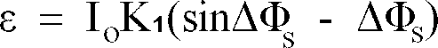
signal generator 27 on the basis of the output V₁ and is added with the output V₂ of the low-pass filter 26 in anadder 29. The output Vs of theadder 29 is expressed by the following equation: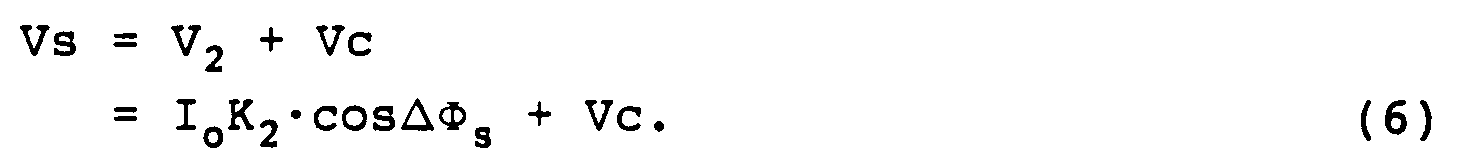
The correcting signal Vc is given by the following polynomial of high order:

The output Vs of theadder 29 is supplied to adifferential amplifier 31, wherein it is differentially operated with a reference voltage VR from areference voltage generator 32. The error output Ve of thedifferential amplifier 31 is given by the following equation:
where it is assumed that K₁ and K₂ are pre-adjusted so that
- The output Ve of the
differential amplifier 31 is applied to an integratingfilter 33. The output of the integratingfilter 33 is provided to alight source driver 23 which controls the quantity of light which is emitted from thelight source 11. Thus, the quantity of light I from thelight source 11 is controlled. Assuming that
differential amplifier 31 is zero when no angular rate is being applied, that is, when the phase difference ΔΦs between the CW and CCW light beams in theoptical fiber coil 15 is zero. Suppose that the quantity of light Io reaching thephotodetector 17 has decreased due to an ambient temperature change. As a result, the output Ve becomes a positive voltage on the basis of Eq. (8). The positive voltage is applied to the integratingfilter 33, which in turn generates a positive integrated voltage. Thelight source driver 23 is pre-adjusted to increase the quantity of light I of thelight source 11 on the basis of the positive integrated voltage and is controlled so that the input to the integratingfilter 33, that is, the output Ve of thedifferential amplifier 31 is always zero. In consequence, the following equation holds.

The FOG output V₁ that is provided by the operation of the afore-mentioned scale factor stabilizing system is expressed by the following equation on the basis of Eqs. (4) and (9).

Based on Eq. (10), the linearity error Li of the scale factor is given by the following equation:

In Eq. (11), if the correcting signal Vc is zero, the Sagnac phase difference ΔΦs increases and the linearity error also increases, as seen from Fig. 3A which is a graph showing the results of calculation of the linearity error Li. To improve this linearity error, the respective coefficients C₀ to Ck in Eq. (7) expressing the correcting signal Vc are calculated by the least square method so that the numerator in Eq. (11) becomes zero with respect to the Sagnac phase difference ΔΦs. Fig. 3B is a graph showing the results of calculation of the linearity in the case where the correcting signal Vc was produced with coefficients Ck of up to the fourth order through utilization of data of the FOG output V₁ produced when the Sagnac phase difference ΔΦs was within the range of 0 to 40°. - Fig. 4 illustrates in block form a specific operative example of the correcting
signal generator 27 which generates the correcting signal Vc in the case where C₀ = 0 and k = 4 in Eq. (7). At first, the signal V₁ is rendered by anabsolute value circuit 27A into the form of an absolute value. While in this example the value of the signal V₁ is changed into the corresponding absolute value and made independent of the polarity of the input angular rate, the correcting signal Vc could be produced without using such an absolute value representation. In this instance, however, to keep substantially the same accuracy of correction as is obtainable with this example, coefficients of higher order, that is, more multiplier means, are needed. The absolute value output |V₁| is fed to an amplifier 7A1, wherein it is amplified by a factor of C₁ to provide a first-order correcting signal

absolute value circuit 27A, and the multiplied output is further amplified by a factor of C₃ in an amplifier 7A3 to provide a third-order correcting signal

adder 27S and the added output is provided as the linearity correcting signal Vc. In this case, the gains C₁, C₂, C₃ and C₄ of the amplifiers 7A1, 7A2, 7A3 and 7A4 are set to the same values as those of the coefficients in Eq. (7). - Incidentally, the respective coefficients of the correcting signal used to obtain the graph of Fig. 3B are as follows:
- C₁ =
- -0.000109
- C₂ =
- 0.03344
- C₃ =
- -0.000038
- C₄ =
- 0.0000268.
- In the Fig. 2 embodiment the same frequency component as the phase modulation frequency fm is used as the FOG output (i.e. the sine component output) V₁, but other odd harmonic components such as third, fifth, ... harmonic components may also be used. Moreover, the second harmonic component used as the cosine component output V₂ may also be replaced with fourth, sixth, ... and other even harmonic components. Although in the above the output V₂ is extracted by the
synchronous detector 25, it is also possible to selectively extract a second or higher even harmonic component from the output of thephotodetector 17 by a band-pass filter and use the filter output as the output V₂ after rendering it into DC form. - The Fig. 2 embodiment has been described in connection with the case of employing only one cosine component (i.e., even harmonic component) to stabilize the scale factor, but another method for suppressing the FOG output variation which is caused by a change in the quantity of light Io is disclosed in, for example, U.S. Patent No. 4,863,358. According to this method, predetermined sine and cosine components in Eq. (2) are synchronously detected, the squared sum of which is produced to generate the signal Vs such that

light source 11 is controlled so that the signal Vs reaches a fixed reference level. Fig. 5 shows the application of this method to the embodiment of Fig. 2. - In Fig. 5 the outputs V₁ and V₂ from the
synchronous detectors 18 and 25 (which are assumed to include the low-pass filters corresponding to those 19 and 26 in Fig. 2, respectively) are squared bymultipliers adder 28. The output Vs of theadder 28 is given by the following equation:

As described previously with respect to the Fig. 2 embodiment, by setting the respective gains KA1 and KA2 such that

The output Vs of theadder 28 is applied to theadder 29, wherein it is added to the correcting signal Vc expressed by Eq. (7) to produce a signal Vss. The output Vss of theadder 29 is expressed by the following equation, using Eq. (13).

The output Vss of theadder 29 is applied to thedifferential amplifier 31, wherein it is differentially operated with the reference voltage VR from thereference voltage generator 32. The error output Ve of thedifferential amplifier 31 is given by the following equation:

The output Ve of thedifferential amplifier 31 is applied to the integratingfilter 33 and, as is the case with the Fig. 2 embodiment, the integrated output is provided to thelight source driver 23 to control the quantity of light I that is emitted from thelight source 11. Suppose that
optical fiber coil 15, that is, when the phase difference ΔΦs between the CW and CCW light beams in theoptical fiber coil 15 is zero, Vc in Eq. (15) is zero, and hence Ve by Eq. (15) is zero. - Now, let it be assumed that the quantity of light Io reaching the
photodetector 17 has been reduced by a change in the ambient temperature. In this case, the error signal Ve becomes a positive voltage on the basis of Eq. (15). Suppose that this positive voltage is applied to the integratingfilter 33 to generate a positive integrated voltage. Assuming that thelight source driver 23 is so adjusted as to increase the quantity of light from thelight source 11 with the positive integrated voltage, it is controlled so that the input to the integratingfilter 33, that is, the output Ve from thedifferential amplifier 31, is always zero. As a result, the following equation holds:

The FOG output V₁, which is provided by operating such a quantity-of-light control circuit to stabilize the scale factor, is given by the following equation on the basis of Eqs. (4) and (16).
Based on Eq. (17), the linearity error Li is given as follows:

Fig. 6A is a graph showing the linearity error in the case where the correcting signal Vc is zero in Eq. (18). In the generation of the correcting signal Vc to improve the linearity, the respective coefficients C₀ through Ck in Eq. (17) are calculated by the least square method so that the numerator in Eq. (18) may be zero with respect to the Sagnac phase difference ΔΦs, as in the case of the Fig. 2 embodiment. Fig. 6B is a graph showing the linearity error improved by the correcting signal Vc produced with the coefficients C₀ to C₄ of up to fourth order through utilization of data of the FOG output V₁ obtained in the case of the Sagnac phase difference ΔΦs being within the range of from 0 to 40°. Incidentally, the respective coefficients of the correcting signal which are determined by the least square method and used to obtain the graph of Fig. 6B are as follows: - C₀ =
- 0
- C₁ =
- 0.000997
- C₂ =
- -0.3324
- C₃ =
- 0.01106
- C₄ =
- -0.02808.
- Fig. 7 illustrates a modified form of the Fig. 2 embodiment, in which the generation of the correcting signal Vc by the correcting
signal generator 27 is simplified. Based on the fact that, of the aforementioned coefficients C₀ to C₄, the second-order coefficient C₂ is remarkably large as can be seen from their concrete values which provided the results depicted in Figs. 3B and 6B, the correcting signal is generated in the form of
- The correcting
signal generator 27 is made up of amultiplier 27A and anamplifier 27B. The output V₁ of the low-pass filter 19 is squared by themultiplier 27A and is amplified by a factor of C₂ in theamplifier 27B, and the amplified output
pass filter 26. The output Vs of theadder 29 is expressed by the following equation:

By setting the gains KA1 and KA2 such that

The output Vs of theadder 29 is compared, by thedifferential amplifier 31, with the reference voltage VR available from thereference voltage generator 32, by which the error signal Ve is yielded. Since the negative feedback loop operates so that the error signal Ve is reduced to zero, the following equation holds.

By setting

By substituting Eq. (22) for
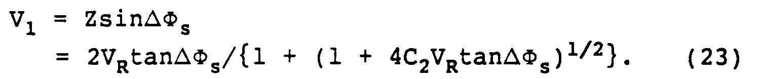
Eq. (23) has nothing to do with the quantity of light Io, and hence the scale factor is stabilized with respect to a temperature change. Furthermore, the linearity is also higher in accuracy than in the case of approximating the FOG output by tanΔΦs alone, since tanΔΦs is corrected by the denominator in Eq. (23) with an appropriate selection of the value C₂. The linearity error Li of the FOG output is given by the following equation:

The coefficient C₂ is computed such that the linearity error is minimum within a predetermined range of the phase difference, and the coefficient is set as the gain of theamplifier 27B in Fig. 7. - In the Fig. 7 embodiment the component of the same frequency as the phase modulation frequency fm is extracted, as the sinΔΦs component, by synchronous detection, but other odd harmonic components such as third, fifth, ... harmonic component may also be extracted. Moreover, the second harmonic component used as the cosΔΦs component may also be replaced with other even harmonic components such as fourth, sixth, ... ones. The cosΔΦs component need not always be extracted by the
synchronous detector 25 but instead it may also be obtained by extracting a desired even harmonic component from the output of thephotodetector 17 through use of a filter and rendering the detected output into DC form. Although in the above only the second-order term in Eq. (7) is used for the correcting signal Vc, other terms can be used. For example, in the case where the accuracy of correction may be sacrificed to some extent, the use of the first-order term CV permits the formation of the correctingsignal generator 27 by only an amplifier. - Fig. 8 illustrates an embodiment according to the second aspect of the present invention. In this embodiment which utilizes a method disclosed in Japanese Patent Application Laid Open No. 62-12811, a third harmonic component is extracted, as the sine component (an odd harmonic component), by the
synchronous detector 18 to obtain the FOG output, and at the same time, second and fourth harmonic components are extracted, as the cosine components (even harmonic components), bysynchronous detectors - A third harmonic component of the phase modulation frequency fm is converted into a DC signal by the
synchronous detector 18 including a low-pass filter using the reference signal Sr from thereference signal generator 24. The output DC signal corresponding to the third harmonic component is provided, with a proper gain, as the FOG output V₃ to theoutput terminal 21. The FOG output V₃ is expressed by the following equation:
where KA3 is the gain of the electrical circuit. - Incidentally, the proportional coefficients (or amplitudes) K₁ and K₃ of the sine components of odd harmonic components which are obtained by synchronous detection as indicated by Eqs. (4) and (25) are dependent on the value of the variable X of the Bessel function as mentioned previously. Hence, in the above-mentioned Japanese Patent Application Laid Open No. 62-12811 an automatic control loop is formed which controls the modulation index A in the
phase modulator 16 so that Bessel functions J₂(X) and J₄(X) are essentially equal to each other, that is, the second and fourth harmonic components in the output of thephotodetector 17 are essentially equal to each other, by performing the phase modulation at the intersection (X = 4.2) of the Bessel functions J₂(X) and J₄(X) where the Bessel function J₃(X) is maximum, as shown in Fig. 9. This will hereinafter be described. - At first, the second harmonic component of the phase modulation frequency in the output of the
photodetector 17, expressed by Eq. (2), is synchronously detected by the synchronous detector 25 (including a low-pass filter) with a reference signal Sr2 of a frequency 2fm and the fourth harmonic component is synchronously detected by the synchronous detector (including a low-pass filter) 41 with a reference signal Sr4 of a frequency 4fm. The respective outputs V₂ and V₄ converted by the synchronous detection into DC levels are expressed by the following equations:
where KA2 and KA4 are gains of electrical circuits. - Next, the output V₂ of the
synchronous detector 25 is fed to a non-inverting input side of adifferential amplifier 42 and the output V₄ of thesynchronous detector 41 is fed to an inverting input side of thedifferential amplifier 42. The output of thedifferential amplifier 42 is applied to anintegrator 43. Thephase modulation driver 22 has a construction such that it increases the modulation index A and consequently the value X by increasing, on the basis of a positive signal from theintegrator 43, the voltage of the modulator drive signal Sp of the drive frequency fm which is applied to thephase modulator 16 and that it decreases the modulation index A and consequently the value X by decreasing, on the basis of a negative signal from theintegrator 43, the voltage of the modulator drive signal Sp of the drive frequency fm which is applied to thephase modulator 16. Themodulation driver 22 constitutes the above-mentioned automatic control loop. Thus, in this embodiment the voltage of the modulator drive signal Sp which is fed to thephase modulator 16 is controlled by themodulator driver 22 so that when the output of thedifferential amplifier 42 is zero, that is, when
- The value of the Bessel function J₃(X) can be stabilized by fixing the value X as mentioned above, but the optical loss Kop in Eq. (25) which expresses the FOG output V₃ is likely to vary around 30% with a temperature change within the range of -20°C to +70°C. In view of this, according to the present invention, the second and fourth harmonic component outputs V₂ and V₄ of the
synchronous detectors light source 11 or the gain of the output from thephotodetector 17 is controlled so that the added output (hereinafter referred to as a composite cosine component) becomes equal to the reference voltage. That is, the synchronous detector outputs V₄ is amplified by a factor of Km in anamplifier 44 and is then added to the synchronous detector output V₂ in theadder 28. The composite cosine component Vs which is the output of theadder 28 is expressed by the following equation:

Now, pre-adjusting the gains KA3 and KA4 such that

Now, calculating the bracketed value F(X) in Eq. (29) with Km set to 2.06, it is maximum at the position where X = 4.20 as indicated by the curve F(X) in Fig. 9 and the value F(X) is stable with respect to a variation in X at the peak of the curve. That is, the Bessel function J₃(X) which is used in the FOG output also becomes maximum at the same position as that where the value F(X) is maximum. Accordingly, the composite cosine component Vs given by Eq. (29) can be used as a cosΔΦs component stable with respect to the value X in the fiber optic gyro which has an operating point of X = 4.20. The output Vs of theadder 28, which is stable with respect to the value X, is differentially operated by thedifferential amplifier 31 with the reference voltage VR from thereference voltage generator 32. The output Ve of thedifferential amplifier 31 is given as follows:
The output Ve of thedifferential amplifier 31 is applied to the integratingfilter 33 and its output is fed to thelight source driver 23 to control the quantity of light I that is emitted from thelight source 11. Assuming that
optical fiber coil 15, that is, the phase difference ΔΦs between the CW and CCW light beams in theoptical fiber coil 15 is zero. Now, suppose that the quantity of light Io which reaches thephotodetector 17 has been decreased owing to an ambient temperature change. In such an instance, the output Ve becomes a positive voltage. Let it be assumed that the integratingfilter 33 yields a positive integrated voltage when supplied with the positive voltage. Thelight source driver 23 is so constructed as to increase the quantity of light from thelight source 11 by the application of the positive integrated voltage, and it is controlled so that the input to the integratingfilter 33, that is, the output Ve of thedifferential amplifier 31 is always zero. In consequence, the following equation holds:

Hence, by setting

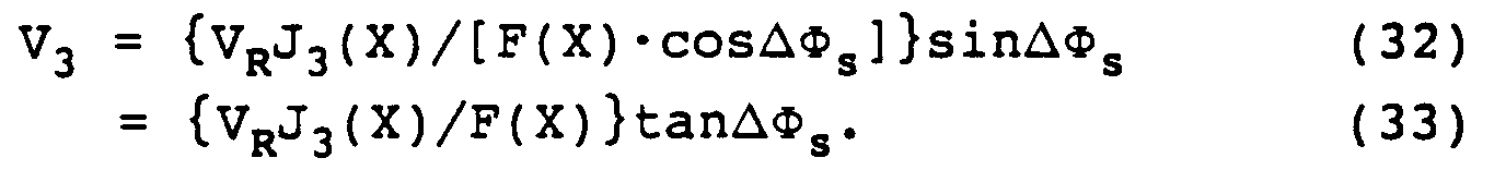
As is evident from Eq. (32), the FOG output V₃ does not include the term of the quantity of light Io reaching thephotodetector 17 nor does it include the gains KA2, KA3, KA4, Kop, Kpd, etc. which have temperature dependence. In addition, since the value X is also fixed as referred to previously, it is possible to offer a fiber optic gyro which has a scale factor stable with respect to ambient temperature changes. - Incidentally, in the construction of Fig. 8, since the FOG output V₃ is obtained as a value proportional to the tanΔΦs component as expressed by Eq. (33), the linearity of the FOG output with respect to the input angular rate Ω is particularly poor when the input angular velocity is large. Fig. 10 shows the principal part of a modified form of the Fig. 8 embodiment which is intended to improve the linearity of the FOG output.
- In the construction depicted in Fig. 10, the FOG output V₃ and the output Vs of the
adder 28 in Fig. 8 are squared bymultipliers adder 29. Themultiplier 27 performs the function of the correctingsignal generator 27 in the Fig. 7 embodiment and squares the FOG output V₃ and outputs it as the correcting signal Vc. The output Vss ofadder 29 is expressed by the following equation:

In this case, the respective gains are initialized such that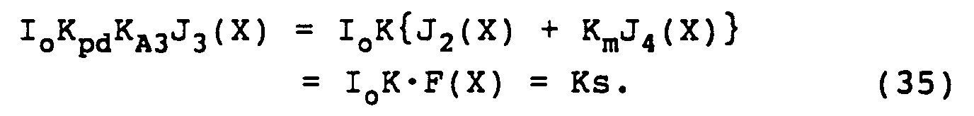
The output Vss of theadder 29 is compared by thedifferential amplifier 31 with the reference voltage VR from thereference voltage generator 32, and the resulting error signal Ve is fed to the integratingfilter 33. The output of the integratingfilter 33 is supplied to thelight source driver 23 to form a negative feedback control loop so that the error Ve is reduced to zero, providing

As can be seen from Eq. (36), the FOG output V₃ is stabilized independently of the quantity of light Io. In addition, the sinΔΦs component is higher than the tanΔΦs component in the accuracy of approximation to the value of the phase difference ΔΦs and provides the FOG output of an excellent linearity. Hence, the FOG output obtainable with the Fig. 10 embodiment is more excellent in linearity than the FOG output in the Fig. 8 embodiment which is expressed by Eq. (33). - Fig. 11 illustrates the principal part of another modification corresponding to the Fig. 10 embodiment. As in the case of Fig. 7, the FOG output V₃ is squared by the
multiplier 27A and the multiplied output is amplified by a factor C₂ in theamplifier 27B to obtain the signal Vc, which is applied as a correcting signal to theadder 29, wherein it is added to the composite cosine component Vs from the adder 28 (Fig. 8). The output Vss of theadder 29 is expressed by the following equation:

By pre-adjusting and setting respective gains so that Eq. (35) holds as is the case with Fig. 10, Eq. (37) is expressed as follows:

The output Vss from theadder 29 is compared by thedifferential amplifier 31 with the reference voltage VR from thereference voltage generator 32, and the resulting error signal Ve is fed to the integratingfilter 33. The output of the integratingfilter 33 is supplied to thelight source driver 23 to form the negative feedback control loop, providing
- Fig. 12 illustrates in block form the principal part of still another modification corresponding to the Fig. 11 embodiment. The correcting
signal generator 27 is comprised of anabsolute value circuit 27C and anamplifier 27B, and only the first-order term C₁V in Eq. (7) is used. The FOG output V₃ is rendered by theabsolute value circuit 27A into an absolute value, which is amplified by a factor of C₁ in theamplifier 27B to obtain the correcting signal Vc. The correcting signal Vc and the output Vs from the adder 28 (Fig. 8) are added together by theadder 29. The output Vss of theadder 29 is expressed by the following equation:

By pre-adjusting and setting respective gains so that Eq. (35) holds as in the case of the Fig. 10 embodiment, Eq. (39) is given as follows:

The output Vss from theadder 29 is compared by thedifferential amplifier 31 with the reference voltage VR from thereference voltage generator 32 as in the above, and the resulting error signal Ve is provided to the integratingfilter 33. The output of the integratingfilter 33 is applied to thelight source driver 23, establishing a feedback control loop which operates so that the error signal Ve is reduced to zero. Accordingly, the FOG output V₃ is expressed by the following equation:

As will be appreciated from Eq (41), also in this embodiment the FOG output has nothing to do with the quantity of light Io, and hence the scale factor is stable. Moreover, the linearity can be improved by a suitable selection of the coefficient C₁. - In the embodiments of Figs. 8, 10, 11 and 12 the output of the integrating
filter 33 is fed back to thelight source driver 23, but the same results as those described above could also be obtained by employing a construction wherein the automaticgain control circuit 39 is disposed at the output stage of thephotodetector 17 as indicated by the broken line in Fig. 8 and the output of the integratingfilter 33 is fed back to the automaticgain control circuit 39 to control its gain. In the embodiments of Figs. 11 and 12 theamplifier 27B may also be inserted in the path of the signal Vs as indicated by the broken line. - In the above-described embodiments the
optical couplers phase modulator 16 may also be formed by optical IC's. - As described above, according to the first aspect of the present invention, the sine and cosine components of the Sagnac phase difference ΔΦs are detected from the output of the
photodetector 17, the sine component is provided as the FOG output, the correcting signal is derived from the sine component, the cosine component is used to form a feedback loop for stabilizing the scale factor, and the correcting signal is introduced into the feedback loop. By this, the linearity of the FOG output can be improved. According to the second aspect of the present invention, the sine component and two cosine components of the Sagnac phase difference ΔΦs in the output of thephotodetector 17 are detected and the sine component is used as the FOG output. On the other hand, by controlling the modulation index of thephase modulator 16 so that the two cosine components are equal to each other, the variable X of the Bessel function is fixed at a constant value, and by adding the two cosine components at a predetermined ratio, the composite cosine component is produced. The composite cosine component is used to form the feedback loop for stabilizing the scale factor, by which it is possible to make the scale factor stable with respect to a temperature change. - It will be apparent that many modifications and variations may be effected without departing from the scope of the novel concepts of the present invention.
Claims (16)
- An optical-interference-type angular rate sensor wherein light from light source means is branched by branch means into clockwise and counterclockwise light beams for propagation through an optical path forming at least one loop, said clockwise and counterclockwise light beams, after having propagated through said optical path, are caused by interference means to interfere with each other, said clockwise and counterclockwise light beams are phase modulated by phase modulator means disposed between said branch means and one end of said optical path, the intensity of the interference light is detected by photodetector as an electrical signal, and a sine component of a Sagnac phase difference ΔΦs which is caused by an angular rate applied to said optical path around its axis is demodulated by first demodulator means from said electrical signal, thereby detecting said angular rate, said optical-interference-type angular rate sensor comprising:
second demodulator means for demodulating a cosine component of said Sagnac phase difference ΔΦs from said electrical signal;
means for generating a scale factor stabilizing signal on the basis of said cosine component from said second demodulator means;
correcting signal generating means for generating a correcting signal on the basis of said sine component;
adder means for adding said correcting signal to said scale factor stabilizing signal;
reference value generating means for generating a reference value;
comparator means for comparing the output of said adder means with said reference value and for generating an error signal; and
feedback loop means whereby the level of said electrical signal that is applied to said first and second demodulator means is controlled so that said error signal is reduced to zero. - The angular rate sensor of claim 1, wherein said scale factor stabilizing signal generating means is means for extracting said cosine component from said second demodulator means and for providing it to said adder means.
- The angular rate sensor of claim 1, wherein said scale factor stabilizing signal generating means is means for generating the squared sum of said cosine and sine components and for providing it to said adder means.
- The angular rate sensor of claim 1, wherein said correcting signal generating means is means for generating said correcting signal in accordance with a polynomial of a predetermined degree of high order using said sine component as a variable.
- The angular rate sensor of claim 1, wherein said correcting signal generating means is means for multiplying the square of said sine component by a predetermined factor and for outputting it as said correcting signal.
- The angular rate sensor of claim 1, wherein said correcting signal generating means is means for multiplying the absolute value of said sine component by a predetermined factor and for outputting it as said correcting signal.
- The angular velocity sensor of claim 1, wherein said light source means includes a light source for emitting said light and a light source driver for driving said light source, and said feedback loop is means for controlling said light source driver on the basis of said error signal to thereby control the quantity of light that is emitted from said light source.
- The angular velocity sensor of claim 1, wherein said feedback loop means includes gain control means inserted at the output side of said photodetector means, said feedback loop means being means for controlling said gain control means on the basis of said error signal to thereby control the level of the output electrical signal of said photodetector means.
- An optical-interference-type angular rate sensor wherein light from a light source is branched into clockwise and counterclockwise light beams for propagation through an optical path forming at least one loop, said clockwise and counterclockwise light beams, after having propagated through said optical path, are caused by interference means to interfere with each other, said clockwise and counterclockwise light beams are phase modulated by phase modulator means disposed between said branch means and one end of said optical path, the intensity of the interference light is detected by photodetector means as an electrical signal, and a sine component of a Sagnac phase difference ΔΦs which is caused by an angular rate applied to said optical path around its axis is demodulated by sine component demodulator means from said electrical signal, thereby detecting said angular rate, said optical-interference-type angular rate sensor comprising:
first and second cosine component demodulator means for demodulating first and second cosine components of said Sagnac phase difference ΔΦs from said electrical signal;
first subtractor means for calculating the difference between said first and second cosine components;
modulation control loop means for controlling, on the basis of the output of said first subtractor means, a modulation index of said phase modulator means so that said first and second cosine components become equal to each other;
cosine component combine means for combining said first and second cosine components at a predetermined ratio into a composite cosine component;
comparator means for comparing a signal corresponding to said composite cosine component with a predetermined reference value and for generating an error signal; and
level control feedback loop means whereby the level of said electrical signal which is applied to said first and second cosine component demodulator means and said sine component demodulator means is controlled so that said error signal is reduced to zero. - The angular velocity sensor of claim 9, which further comprises correcting signal generating means for generating a correcting signal on the basis of said sine component and adder means for adding said correcting signal to a signal corresponding to said composite cosine component and for providing the added output to said comparator means.
- The angular velocity sensor of claim 10, wherein said correcting signal generating means is means for outputting the square of said sine component as said correcting means and said adder means is means for adding the square of said composite cosine component, as a signal corresponding to said composite cosine component, to said correcting signal.
- The angular velocity sensor of claim 10, wherein said correcting signal generating means includes means for generating the square of said sine component and said adder means is means for adding the square of said sine component and said composite cosine component at a predetermined ratio and for applying the added output to said comparator means as a signal corresponding to said composite cosine component.
- The angular velocity sensor of claim 10, wherein said correcting signal generating means includes absolute value means for generating the absolute value of said sine component and said adder means is means for adding the output of said absolute value means and said composite cosine component at a predetermined ratio and for applying the added output to said comparator means as a signal corresponding to said composite cosine component.
- The angular velocity sensor of claim 9 or 10, wherein said light source means includes a light source for emitting said light and a light source driver for driving said light source and said level control feedback loop means is means for controlling said light source driver on the basis of said error signal to thereby control the quantity of light that is emitted from said light source.
- The angular velocity sensor of claim 9 or 10, wherein said level control feedback loop means includes gain control means inserted at the output side of said photodetector means, said level control feedback loop means being means for controlling said gain control means on the basis of said error signal to thereby control the level of the output electrical signal of the photodetector means.
- The angular velocity sensor of claim 9 or 10, wherein said first and second cosine components are second and fourth harmonic components of a phase modulation frequency, said sine component is a third harmonic component of said phase modulation frequency and said cosine component combine means is means for adding said first and second cosine components in the ratio 1:2.06 to obtain said composite cosine component.
Applications Claiming Priority (7)
| Application Number | Priority Date | Filing Date | Title |
|---|---|---|---|
| JP121489/92 | 1992-05-14 | ||
| JP4121489A JP2578045B2 (en) | 1992-05-14 | 1992-05-14 | Optical interference angular velocity meter |
| JP13811392A JP2514532B2 (en) | 1992-05-29 | 1992-05-29 | Optical interference gyro |
| JP138113/92 | 1992-05-29 | ||
| JP14428692 | 1992-06-04 | ||
| JP144286/92 | 1992-06-04 | ||
| US08/190,354 US5412472A (en) | 1992-01-30 | 1994-02-01 | Optical-interference type angular velocity or rate sensor having an output of improved linearity |
Publications (2)
| Publication Number | Publication Date |
|---|---|
| EP0569993A1 true EP0569993A1 (en) | 1993-11-18 |
| EP0569993B1 EP0569993B1 (en) | 1996-01-31 |
Family
ID=27470782
Family Applications (1)
| Application Number | Title | Priority Date | Filing Date |
|---|---|---|---|
| EP93107836A Expired - Lifetime EP0569993B1 (en) | 1992-05-14 | 1993-05-13 | Optical-interference-type angular rate sensor |
Country Status (1)
| Country | Link |
|---|---|
| EP (1) | EP0569993B1 (en) |
Cited By (5)
| Publication number | Priority date | Publication date | Assignee | Title |
|---|---|---|---|---|
| WO1996041130A1 (en) * | 1995-06-07 | 1996-12-19 | Honeywell Inc. | Optical power balancing in an interferometric fiber optic gyroscope |
| WO1998058235A1 (en) * | 1997-06-19 | 1998-12-23 | Honeywell Inc. | Fiber optic gyroscope vibration error compensator |
| WO1998058234A1 (en) * | 1997-06-19 | 1998-12-23 | Honeywell Inc. | Vibration error reduction servo for a fiber optic gyroscope |
| WO1999035467A3 (en) * | 1997-12-31 | 1999-09-10 | Honeywell Inc | Fiber optic gyroscope |
| EP2860119A1 (en) | 2013-10-09 | 2015-04-15 | Multivac Sepp Haggenmüller GmbH & Co. KG | Deep draw packaging machine and method |
Citations (2)
| Publication number | Priority date | Publication date | Assignee | Title |
|---|---|---|---|---|
| US5048961A (en) * | 1989-03-08 | 1991-09-17 | Sumitomo Electric Industries, Ltd. | Phase modulated fiber-optic gyroscope for measuring the angular velocity of a moving object |
| EP0454113A2 (en) * | 1990-04-26 | 1991-10-30 | Hitachi, Ltd. | Optical fiber gyroscope |
-
1993
- 1993-05-13 EP EP93107836A patent/EP0569993B1/en not_active Expired - Lifetime
Patent Citations (2)
| Publication number | Priority date | Publication date | Assignee | Title |
|---|---|---|---|---|
| US5048961A (en) * | 1989-03-08 | 1991-09-17 | Sumitomo Electric Industries, Ltd. | Phase modulated fiber-optic gyroscope for measuring the angular velocity of a moving object |
| EP0454113A2 (en) * | 1990-04-26 | 1991-10-30 | Hitachi, Ltd. | Optical fiber gyroscope |
Cited By (7)
| Publication number | Priority date | Publication date | Assignee | Title |
|---|---|---|---|---|
| WO1996041130A1 (en) * | 1995-06-07 | 1996-12-19 | Honeywell Inc. | Optical power balancing in an interferometric fiber optic gyroscope |
| WO1998058235A1 (en) * | 1997-06-19 | 1998-12-23 | Honeywell Inc. | Fiber optic gyroscope vibration error compensator |
| WO1998058234A1 (en) * | 1997-06-19 | 1998-12-23 | Honeywell Inc. | Vibration error reduction servo for a fiber optic gyroscope |
| US5923424A (en) * | 1997-06-19 | 1999-07-13 | Honeywell Inc. | Fiber optic gyroscope vibration error compensator |
| US5926275A (en) * | 1997-06-19 | 1999-07-20 | Honeywell Inc. | Vibration error reduction servo for a fiber optic gyroscope |
| WO1999035467A3 (en) * | 1997-12-31 | 1999-09-10 | Honeywell Inc | Fiber optic gyroscope |
| EP2860119A1 (en) | 2013-10-09 | 2015-04-15 | Multivac Sepp Haggenmüller GmbH & Co. KG | Deep draw packaging machine and method |
Also Published As
| Publication number | Publication date |
|---|---|
| EP0569993B1 (en) | 1996-01-31 |
Similar Documents
| Publication | Publication Date | Title |
|---|---|---|
| JP2510460B2 (en) | Method and device for measuring rotational speed | |
| US8830479B2 (en) | RFOG with optical heterodyning for optical signal discrimination | |
| EP0730725A1 (en) | Reduction of optical noise | |
| JPS62108110A (en) | Optical fiber gyro | |
| US4948252A (en) | Sub-tau phase modulation in a fiber-optic rotation sensor | |
| US5412472A (en) | Optical-interference type angular velocity or rate sensor having an output of improved linearity | |
| EP0569993B1 (en) | Optical-interference-type angular rate sensor | |
| EP0431474B1 (en) | Fiber optic gyro | |
| JP2808188B2 (en) | Demodulation reference signal source | |
| US7324206B2 (en) | Method for determination/compensation of bias errors/random walk errors induced by the light source in fiber-optic Sagnac interferometers | |
| JPH11108669A (en) | Fiber optic gyro | |
| JP2578045B2 (en) | Optical interference angular velocity meter | |
| JPS6212811A (en) | Angular speed meter using optical interference | |
| JP2514532B2 (en) | Optical interference gyro | |
| EP0492580B1 (en) | Fiber optic gyro | |
| JP2548072B2 (en) | Optical interference gyro | |
| JPH0558486B2 (en) | ||
| JPH10132578A (en) | Optical fiber gyroscope | |
| JP2619015B2 (en) | Fiber optic gyro | |
| JP2649310B2 (en) | Optical interference gyro with self-diagnosis function | |
| JP2739191B2 (en) | Optical interference angular velocity meter | |
| JP3271019B2 (en) | Fiber optic gyro | |
| JP2961335B2 (en) | Fiber optic gyro | |
| JPH09269230A (en) | Optical interference angular velocity meter | |
| JPS61235719A (en) | Fiber interferometer |
Legal Events
| Date | Code | Title | Description |
|---|---|---|---|
| PUAI | Public reference made under article 153(3) epc to a published international application that has entered the european phase |
Free format text: ORIGINAL CODE: 0009012 |
|
| 17P | Request for examination filed |
Effective date: 19930518 |
|
| AK | Designated contracting states |
Kind code of ref document: A1 Designated state(s): DE FR GB |
|
| 17Q | First examination report despatched |
Effective date: 19950515 |
|
| GRAA | (expected) grant |
Free format text: ORIGINAL CODE: 0009210 |
|
| AK | Designated contracting states |
Kind code of ref document: B1 Designated state(s): DE FR GB |
|
| REF | Corresponds to: |
Ref document number: 69301424 Country of ref document: DE Date of ref document: 19960314 |
|
| ET | Fr: translation filed | ||
| PLBE | No opposition filed within time limit |
Free format text: ORIGINAL CODE: 0009261 |
|
| 26N | No opposition filed | ||
| REG | Reference to a national code |
Ref country code: GB Ref legal event code: IF02 |
|
| PGFP | Annual fee paid to national office [announced via postgrant information from national office to epo] |
Ref country code: FR Payment date: 20110523 Year of fee payment: 19 |
|
| PGFP | Annual fee paid to national office [announced via postgrant information from national office to epo] |
Ref country code: GB Payment date: 20110511 Year of fee payment: 19 |
|
| PGFP | Annual fee paid to national office [announced via postgrant information from national office to epo] |
Ref country code: DE Payment date: 20110511 Year of fee payment: 19 |
|
| GBPC | Gb: european patent ceased through non-payment of renewal fee |
Effective date: 20120513 |
|
| REG | Reference to a national code |
Ref country code: FR Ref legal event code: ST Effective date: 20130131 |
|
| REG | Reference to a national code |
Ref country code: DE Ref legal event code: R119 Ref document number: 69301424 Country of ref document: DE Effective date: 20121201 |
|
| PG25 | Lapsed in a contracting state [announced via postgrant information from national office to epo] |
Ref country code: GB Free format text: LAPSE BECAUSE OF NON-PAYMENT OF DUE FEES Effective date: 20120513 Ref country code: FR Free format text: LAPSE BECAUSE OF NON-PAYMENT OF DUE FEES Effective date: 20120531 |
|
| PG25 | Lapsed in a contracting state [announced via postgrant information from national office to epo] |
Ref country code: DE Free format text: LAPSE BECAUSE OF NON-PAYMENT OF DUE FEES Effective date: 20121201 |