EP0576168A1 - Digitaler Phasenregelkreis - Google Patents
Digitaler Phasenregelkreis Download PDFInfo
- Publication number
- EP0576168A1 EP0576168A1 EP93304386A EP93304386A EP0576168A1 EP 0576168 A1 EP0576168 A1 EP 0576168A1 EP 93304386 A EP93304386 A EP 93304386A EP 93304386 A EP93304386 A EP 93304386A EP 0576168 A1 EP0576168 A1 EP 0576168A1
- Authority
- EP
- European Patent Office
- Prior art keywords
- phase
- clock
- delay
- down counter
- output
- Prior art date
- Legal status (The legal status is an assumption and is not a legal conclusion. Google has not performed a legal analysis and makes no representation as to the accuracy of the status listed.)
- Granted
Links
- 238000012544 monitoring process Methods 0.000 claims abstract description 11
- 238000004519 manufacturing process Methods 0.000 claims abstract description 9
- 230000007613 environmental effect Effects 0.000 claims abstract description 5
- 238000005070 sampling Methods 0.000 claims description 14
- 239000013078 crystal Substances 0.000 claims description 4
- 230000001934 delay Effects 0.000 claims description 4
- 230000003111 delayed effect Effects 0.000 claims description 4
- 239000004065 semiconductor Substances 0.000 claims description 2
- 229910052710 silicon Inorganic materials 0.000 abstract description 9
- 239000010703 silicon Substances 0.000 abstract description 9
- 230000010363 phase shift Effects 0.000 abstract description 8
- XUIMIQQOPSSXEZ-UHFFFAOYSA-N Silicon Chemical compound [Si] XUIMIQQOPSSXEZ-UHFFFAOYSA-N 0.000 description 8
- 238000013461 design Methods 0.000 description 8
- 238000013459 approach Methods 0.000 description 6
- 238000010586 diagram Methods 0.000 description 5
- 238000013519 translation Methods 0.000 description 5
- 238000004891 communication Methods 0.000 description 4
- 238000012937 correction Methods 0.000 description 4
- 238000012546 transfer Methods 0.000 description 4
- 238000000034 method Methods 0.000 description 3
- 230000005540 biological transmission Effects 0.000 description 2
- 230000007704 transition Effects 0.000 description 2
- 230000001960 triggered effect Effects 0.000 description 2
- 238000004364 calculation method Methods 0.000 description 1
- 239000003990 capacitor Substances 0.000 description 1
- 230000001413 cellular effect Effects 0.000 description 1
- 230000000295 complement effect Effects 0.000 description 1
- 238000010276 construction Methods 0.000 description 1
- 230000007423 decrease Effects 0.000 description 1
- 230000000694 effects Effects 0.000 description 1
- 230000010354 integration Effects 0.000 description 1
- 238000013139 quantization Methods 0.000 description 1
- 238000012552 review Methods 0.000 description 1
- 239000000758 substrate Substances 0.000 description 1
Images

Classifications
-
- H—ELECTRICITY
- H03—ELECTRONIC CIRCUITRY
- H03L—AUTOMATIC CONTROL, STARTING, SYNCHRONISATION OR STABILISATION OF GENERATORS OF ELECTRONIC OSCILLATIONS OR PULSES
- H03L7/00—Automatic control of frequency or phase; Synchronisation
- H03L7/06—Automatic control of frequency or phase; Synchronisation using a reference signal applied to a frequency- or phase-locked loop
- H03L7/08—Details of the phase-locked loop
- H03L7/099—Details of the phase-locked loop concerning mainly the controlled oscillator of the loop
- H03L7/0991—Details of the phase-locked loop concerning mainly the controlled oscillator of the loop the oscillator being a digital oscillator, e.g. composed of a fixed oscillator followed by a variable frequency divider
-
- H—ELECTRICITY
- H03—ELECTRONIC CIRCUITRY
- H03L—AUTOMATIC CONTROL, STARTING, SYNCHRONISATION OR STABILISATION OF GENERATORS OF ELECTRONIC OSCILLATIONS OR PULSES
- H03L7/00—Automatic control of frequency or phase; Synchronisation
- H03L7/06—Automatic control of frequency or phase; Synchronisation using a reference signal applied to a frequency- or phase-locked loop
- H03L7/08—Details of the phase-locked loop
- H03L7/081—Details of the phase-locked loop provided with an additional controlled phase shifter
-
- H—ELECTRICITY
- H04—ELECTRIC COMMUNICATION TECHNIQUE
- H04L—TRANSMISSION OF DIGITAL INFORMATION, e.g. TELEGRAPHIC COMMUNICATION
- H04L7/00—Arrangements for synchronising receiver with transmitter
- H04L7/02—Speed or phase control by the received code signals, the signals containing no special synchronisation information
- H04L7/033—Speed or phase control by the received code signals, the signals containing no special synchronisation information using the transitions of the received signal to control the phase of the synchronising-signal-generating means, e.g. using a phase-locked loop
- H04L7/0337—Selecting between two or more discretely delayed clocks or selecting between two or more discretely delayed received code signals
Definitions
- the present invention generally relates to phase locked loops (PLLs) and, more particularly, to an improved high speed digital phased locked loop (DPLL) which has a fixed bandwidth independent of variations in manufacturing process or environment and which is programmable to allow user control of phase shifting of the retiming clock.
- PLLs phase locked loops
- DPLL digital phased locked loop
- Digital communication systems provide links not only between various digital devices such as computers connected in a network but also in more traditional electronic communications as well.
- digital devices such as computers connected in a network
- next generation of cellular telephone systems will be digital, and proposals for an all digital high definition television standar are currently under review.
- it is important to minimize the jitter rate of the received pulses and thereby substantially reduce the bit error rate (BER) of a received digital transmission.
- BER bit error rate
- phase locked loops have been used for precise tuning in communications systems.
- the principles of the PLL have been applied to digital communication systems in the form of a digital phase locked loop (DPLL) manufactured as an integrated circuit (IC) on a silicon substrate.
- DPLL digital phase locked loop
- the manufacturing process may introduce subtle variations in DPLL chips.
- timing variations do not alter the function of a module.
- performance characteristics of high speed digital phase locked loops (DPLLs) using tapped delay lines are greatly affected by propagation delays. When considering manufacturing and environmental variations, it is not uncommon to observe a three fold variation between best case and worst case propagation delays.
- U.S. Patent No. 4,626,798 to Fried discloses a phase locked loop wherein the frequency of the ring oscillator in the PLL is adjusted by controlling the number of delay elements in the ring. Fried employs analog circuitry for this control and, therefore, his approach is not easily implemented using very large scale integration (VLSI) techniques.
- VLSI very large scale integration
- a similar approach was taken by Herzog in U.S. Patent No. 4,052,673.
- U.S. Patents No. 4,677,648 to Zurfluh and No. 4,972,444 to Melrose et al. disclose the use of delay lines used in DPLLs. These designs rely on non-return to zero (NRZ) code and have fixed low pass filter elements.
- NRZ non-return to zero
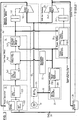
- a digital phase locked loop module integrated on a single semiconductor chip comprising: a phase detector, a low pass filter and a digitally controlled oscillator connected in a loop with said digitally controlled oscillator arranged to generate a system clock output and said phase detector being arranged to compare said system clock output with input digital data; speed monitoring means responsive to said system clock output to sense variations in module speed due to manufacturing and environmental conditions and to generate a first control digital word for application to said low pass filter to adjust dynamic characteristics of the filter; bandwidth regulator means connected to receive said first control digital word from said speed monitoring means and adapted to generate a second control digital word for application to said low pass filter to set a threshold to determine when to make a phase adjustment in said digitally controlled oscillator output; a second, slave digitally controlled oscillator responsive to said system clock for generating a sampling clock; programmable phase shifter means responsive to said low pass filter and said first control digital word from said speed monitoring means for controlling the frequency of said second, slave digitally controlled oscillator; and retiming
- the DPLL digital phase locked loop
- the DPLL includes a phase detector 12, which receives input data, a low pass filter 14 which filters the output of the phase detector 12, and a digitally controlled oscillator (DCO) 16 which receives a precision frequency reference from crystal oscillator 17 and generates a feedback clock signal on line 18 to the phase detector 12.
- DCO digitally controlled oscillator
- the present invention optimizes the performance of the DPLL by addressing two features of this basic design.
- the invention optimizes the DPLL bandwidth by making it independent of the manufacturing process and temperature and power variations.
- a phase shift control is provided to allow the user to control the phase shifting of a retiming latch.
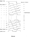
- the DPLL In order to achieve the optimized bandwidth, the DPLL must know the propagation delay through the logic gates. This is referred to as the "silicon speed" of the module and is determined by the module speed monitor 20. The monitor uses this information to adjust the low pass filter characteristics of low pass filter 14. The "speed” indicator is also used to determine the last delay element to use for phase corrections. As the speed of the silicon changes, the number of delay elements required to span a clock cycle changes. The module speed monitor 20 takes snapshots of a delay string or ring oscillator and determines the number of delay elements required to span one full clock period. This is done with the aid of the system clock that is running close to the received data rate and a plurality of latches connected to corresponding delay elements in a delay string.
- the latches asynchronously latch delayed versions of the delay string thereby creating a large register string of binary "1's" and "0's” as shown in Figure 2.
- register contents 0000x1...11100 shown in Figure 2 for example, it takes n+2 delay elements to span one clock period. Monitoring a ring oscillator would require multiple snapshots and additional computation.
- This information is encoded and sent to the low pass filter 14 so that it can determine how many delay elements to use in the delay string or ring oscillator forming the DCO 16.
- the information is also sent to a bandwidth regulator 22 which converts the values dynamically and then feeds it to another section on the low pass filter 14 so that the loop dynamics can be adjusted.
- the low pass filter 14 regulates the speed of the DPLL by telling the DCO 16 when to make a phase adjustment.
- the phase detector 12 provides lag/lead information which is fed to an up/down counter in the low pass filter 14.
- the up/down counter reaches a limit or threshold as determined by the bandwidth regulator 22, the low pass filter causes the DCO 16 to make a phase adjustment.
- This phase adjustment is made in delay strings by selecting a new delay element. For the implementation of the DCO 16 as a ring oscillator, this is done by adding or subtracting a delay element to the ring momentarily.
- the bandwidth regulator In order for the loop to have a fixed bandwidth, the bandwidth regulator must adjust the low pass filter counter threshold dynamically.
- the simplest translation would be to select one threshold value for delay sizes greater than a predefined value and another threshold value for delay sizes less than the predefined value. This approach minimizes hardware requirements but does not perfectly optimize bandwidth. Therefore, the preferred embodiment of the invention employs a lookup table similar to the translation table below: Translation Table Module Speed (Delay Elements) Threshold Count 07 50 08 44 09 39 10 35 11 32 12 29 13 27 14 25 15 23 16 22 17 21 18 19 19 18 20 18 21 17
- the DPLL shown in Figure 1 also contains a second, slave digitally controlled oscillator (DCO) 24.
- This DCO receives as its reference the system clock and is controlled by the phase shifter 26.
- the phase shifter 26 reads the module speed monitor 20 and creates a phase offset control word. This is used by the DCO 24 to create a phase offset sampling clock which is supplied to the retiming latch 28.
- the retiming latch 28 thus retimes the input data with a phase shifted version of the original clock.
- This design is especially useful for retiming return to zero (RZ) code but can also be used for non-return to zero (NRZ) code.
- RZ return to zero
- NRZ non-return to zero
- One reason to use this approach with NRZ code as opposed to selecting the inverted version of the PLL clock is that the retiming clock may not have a tightly controlled duty cycle. Employing this approach removes the dependency on precise 50% duty cycles.
- the phase detector 12 comprises a phase detector circuit 121 and a 180_ check circuit 122, both of which receive the input data and the fed back system clock from the DCO 16. The outputs of these two circuits are supplied to a lag/lead generator 123.
- the phase detector circuit 121 is a D-type latch where the clock input comes from the received data and the data input comes from the output clock of the DCO 16.
- a second latch is used as the check circuit 122 to help prevent the PLL from coming into lock 180_ out of phase. While this is a highly unstable state, it does insure that temporary false locks are avoided such as during module power up. It also becomes more important when the low pass filter is set to a high filter level.
- This second latch uses the same received data as its clock input but uses a slightly delayed version (i.e., 2-5_) of the DCO's output clock. This allows for a simple voting scheme between the two latches.
- the second latch will output the opposite value from what it would have, had it been in phase.
- These two D-type latch outputs are compared in a simple Boolean function called the lag/lead generator 123.
- the phase information of the first latch is used. Should the 180_ condition appear, the lag/lead generator forces a "clock leading data" condition.
- the low pass filter 14 includes an up/down counter 141 which increments for leads and decrements for lags. This input comes from the output of the phase detector 12.
- the counter output value is monitored by the magnitude comparator 142.
- the magnitude comparator monitors for when the up/down counter 141 reaches the threshold specified by the bandwidth regulator. Two conditions must be considered, a lagging threshold and a leading threshold. This is satisfied by using the original bandwidth regulator threshold value in addition to generating a two's complement of it. This function is contained in the magnitude comparator.
- the magnitude comparator 142 When the up/down counter 141 has an output value that equals the lagging threshold, the magnitude comparator 142 resets the counter and causes a second up/down counter 143 to increment. When the up/down counter 141 has an output value that equals the leading threshold, the magnitude comparator resets the counter and causes the second up/down counter 143 to decrement.
- the binary output of the second up/down counter 143 is the address used by the DCO 16 to select the correct clock phase.
- the up/down counter 143 is preconditioned by the module speed indicator 20. When the counter needs to decrement below zero, it checks what value is on the module speed indicator bus and uses that value as the new value. When the counter 143 is incrementing, it checks that the current value is not greater than the module speed indicator 20. If it is, the counter is reset to zero. In this way, a seamless phase shift wrap around point is created.
- the first DCO 16 comprises a binary decoder 161 which receives the output from up/down counter 143 and provides an output to control a clock phase select multiplexer 162.
- the multiplexer 162 receives its input from delay string 171 driven by the crystal oscillator 17.
- Figure 2 shows what the output of the delay string would look like.
- This delay string bus is input to the phase selection multiplexer 162 and should be wired such that each delay tap has a similar capacitive load. Care must also be taken when selecting a new phase clock. When selecting a different phase, the multiplexer 162 must change state during a stable high or low period of the clock.
- the decoder 161 is designed to take this into account.
- the module speed monitor 20 measures the speed of the silicon by taking snapshots of the delay string 171 outputs and finding the last non-redundant delay element.
- the delay string snapshot 121 consists of a register triggered by the system clock. Each bit of the register samples a delay string output when triggered, as illustrated in Figure 2.
- the delay tree size generator 122 determines the last non-redundant delay element by finding the "1" to "0" transition in the bits of the snapshot register. This transition point is output as the number of non-redundant delay string elements.
- the bandwidth regulator 22 uses this value to calculate the low pass filter 14 threshold required to maintain the necessary bandwidth for the current module silicon speed. As mentioned previously, the threshold calculation made by the bandwidth regulator 22 could easily be performed using a translation table.
- the phase shifter 26 also receives the output of the delay tree size generator 122. More specifically, the phase constant generator 261 combines the delay tree size with the phase offset factor to create a control signal for the phase offset generator 262. This control signal represents the number of delay elements required to achieve the desired phase offset for the sampling clock.
- the phase offset generator 262 computes the delay string position of the sampling clock by adding the number of required delay elements output by the phase constant generator 261 to the delay string position of the phase comparison clock as indicated by the output of the up/down counter 143. The phase offset generator 262 also ensures that the selected sampling clock will be selected from the output of a non-redundant delay string element.
- the decoder 241 converts the output of the phase offset generator 262 to n selection signals, where n is the number of delay string elements and all but one of the selection signals is false.
- the delay string element corresponding to the true selection signal will be output by the multiplexer 242 as the sampling clock.
- phase shifter 26 Since the required phase offset input to the phase constant generator 261 for the sampling clock will always be constant for a specific application, it can be specified generally and the phase shifter 26 will translate the general value into the number of required delay elements. This translation can be achieved using a lookup table of required delay elements versus delay string sizes; however, multiple tables would be required for a single design to accommodate multiple applications using different phase offsets. For example, two tables would be required to accommodate NRZ code with a 180_ phase shift and RZ code with a 90_ phase shift. As a more flexible approach, the phase offset can be input as a fraction of the clock period and this value multiplied by the delay string size to determine the required number of delay elements. Once the number of delay elements required to do a specific phase shift is computed, it is simply added to the pointer created by the low pass filter pointer.
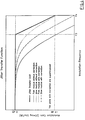
- Figure 4 shows a graph of jitter transfer for the DPLL according to the invention.
- the ratio between the output and input jitter amplitudes of the DPLL is represented in dB, and this ratio is plotted against the frequency of the jitter.
- the graph shows that for a fixed low pass filter threshold, there is a wide variation in the bandwidth of the DPLL. At high frequencies, the slow module will filter mush less jitter than a fast module. However, when the low pass filter threshold is adjusted to compensate for the module silicon speed, the variation in bandwidth between fast and slow modules becomes negligible.
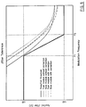
- the amplitude of the phase modulated jitter is expressed in unit intervals (UI).
- UI unit intervals
- One UI is equal to the bit period.
- the curves show that faster silicon cannot handle as high of a jitter amplitude at the lower frequencies. This is because each phase shift is smaller due to faster propagation delays of the delay string. Adjusting the low pass filter threshold by way of the regulator pushes the performance to the right. Note that the difference in performance at the high frequencies between fast and slow modules is due to quantization effects.
Landscapes
- Stabilization Of Oscillater, Synchronisation, Frequency Synthesizers (AREA)
Applications Claiming Priority (2)
| Application Number | Priority Date | Filing Date | Title |
|---|---|---|---|
| US904360 | 1992-06-25 | ||
| US07/904,360 US5313503A (en) | 1992-06-25 | 1992-06-25 | Programmable high speed digital phase locked loop |
Publications (2)
| Publication Number | Publication Date |
|---|---|
| EP0576168A1 true EP0576168A1 (de) | 1993-12-29 |
| EP0576168B1 EP0576168B1 (de) | 1997-04-02 |
Family
ID=25419005
Family Applications (1)
| Application Number | Title | Priority Date | Filing Date |
|---|---|---|---|
| EP93304386A Expired - Lifetime EP0576168B1 (de) | 1992-06-25 | 1993-06-04 | Digitaler Phasenregelkreis |
Country Status (4)
| Country | Link |
|---|---|
| US (1) | US5313503A (de) |
| EP (1) | EP0576168B1 (de) |
| JP (1) | JPH0795685B2 (de) |
| DE (1) | DE69309349D1 (de) |
Cited By (3)
| Publication number | Priority date | Publication date | Assignee | Title |
|---|---|---|---|---|
| WO1995019067A1 (en) * | 1994-01-04 | 1995-07-13 | Level One Communications, Inc. | A digitally controlled first order jitter attenuator using a digital frequency synthesizer |
| FR2818052A1 (fr) * | 2000-12-09 | 2002-06-14 | Zarlink Semiconductor Inc | Procede et dispositif de restauration d'horloge avec boucle a verrouillage de phase a entrees multiples pour commutation de reference sans a-coups |
| EP2288032A3 (de) * | 2001-08-28 | 2013-07-10 | Rambus Inc. | Taktrückgewinnungsschaltung mit wählbarer Phasenregelung |
Families Citing this family (21)
| Publication number | Priority date | Publication date | Assignee | Title |
|---|---|---|---|---|
| US5481573A (en) * | 1992-06-26 | 1996-01-02 | International Business Machines Corporation | Synchronous clock distribution system |
| JP3487309B2 (ja) | 1993-06-30 | 2004-01-19 | 株式会社ルネサステクノロジ | 半導体集積回路装置 |
| US5457719A (en) * | 1993-08-11 | 1995-10-10 | Advanced Micro Devices Inc. | All digital on-the-fly time delay calibrator |
| US5832048A (en) * | 1993-12-30 | 1998-11-03 | International Business Machines Corporation | Digital phase-lock loop control system |
| US5694086A (en) * | 1996-02-28 | 1997-12-02 | Port; Adrian George | Precision, analog CMOS one-shot and phase locked loop including the same |
| US5663992A (en) * | 1996-03-14 | 1997-09-02 | Trimble Navigation Limited | Method and apparatus for correction of GPS carrier phase measurement |
| US6363129B1 (en) * | 1998-11-09 | 2002-03-26 | Broadcom Corporation | Timing recovery system for a multi-pair gigabit transceiver |
| US6424034B1 (en) | 1998-08-31 | 2002-07-23 | Micron Technology, Inc. | High performance packaging for microprocessors and DRAM chips which minimizes timing skews |
| FR2829265A1 (fr) * | 2001-09-04 | 2003-03-07 | St Microelectronics Sa | Detection d'une variation de l'environnement d'un circuit integre |
| US7224759B2 (en) * | 2002-07-11 | 2007-05-29 | Honeywell International Inc. | Methods and apparatus for delay free phase shifting in correcting PLL phase offset |
| US7839178B2 (en) * | 2002-08-20 | 2010-11-23 | Seagate Technology Llc | High speed digital phase/frequency comparator for phase locked loops |
| US20040125903A1 (en) * | 2002-12-31 | 2004-07-01 | Mel Bazes | Digital phase detection with jitter filter |
| US7400690B2 (en) * | 2003-10-14 | 2008-07-15 | Agere Systems Inc. | Adaptive phase controller, method of controlling a phase and transmitter employing the same |
| CN100405239C (zh) * | 2005-12-14 | 2008-07-23 | 苏州科技学院 | 便携式汽车发动机电子模拟装置 |
| US7995698B2 (en) * | 2007-09-28 | 2011-08-09 | Integrated Device Technology, Inc. | Method for binary clock and data recovery for fast acquisition and small tracking error |
| KR101183738B1 (ko) | 2008-05-14 | 2012-09-17 | 재단법인서울대학교산학협력재단 | 공급 전원 변동에 의한 지터 제거 방법 및 이를 적용한 디지털 제어 발진 회로 |
| US7772900B2 (en) * | 2008-07-15 | 2010-08-10 | International Business Machines Corporation | Phase-locked loop circuits and methods implementing pulsewidth modulation for fine tuning control of digitally controlled oscillators |
| US7750701B2 (en) * | 2008-07-15 | 2010-07-06 | International Business Machines Corporation | Phase-locked loop circuits and methods implementing multiplexer circuit for fine tuning control of digitally controlled oscillators |
| KR101220173B1 (ko) * | 2008-12-02 | 2013-01-11 | 한국전자통신연구원 | 주파수 보정루프 |
| US9257994B2 (en) | 2012-03-22 | 2016-02-09 | Amr M. Lotfy | Apparatus and system for digitally controlled oscillator |
| JP6988839B2 (ja) * | 2019-02-01 | 2022-01-05 | オムロン株式会社 | 共振型コンバータ制御回路とその制御方法及び共振型コンバータ |
Citations (4)
| Publication number | Priority date | Publication date | Assignee | Title |
|---|---|---|---|---|
| US4988960A (en) * | 1988-12-21 | 1991-01-29 | Yamaha Corporation | FM demodulation device and FM modulation device employing a CMOS signal delay device |
| US5068628A (en) * | 1990-11-13 | 1991-11-26 | Level One Communications, Inc. | Digitally controlled timing recovery loop |
| US5075640A (en) * | 1990-03-09 | 1991-12-24 | Kabushiki Kaisha Toshiba | Phase locked loop circuit responding to supplied signal frequency |
| EP0475468A2 (de) * | 1984-01-03 | 1992-03-18 | Motorola, Inc. | Phasenkomparator für eine digitale Phasenregelschleife |
Family Cites Families (9)
| Publication number | Priority date | Publication date | Assignee | Title |
|---|---|---|---|---|
| US4052673A (en) * | 1976-08-30 | 1977-10-04 | Rca Corporation | Combined controlled oscillator and frequency multiplier |
| JPS6016145B2 (ja) * | 1979-03-20 | 1985-04-24 | 株式会社日立製作所 | クロツク信号抽出方式 |
| EP0185779B1 (de) * | 1984-12-21 | 1990-02-28 | International Business Machines Corporation | Digitale Phasenregelschleife |
| US4626798A (en) * | 1985-12-11 | 1986-12-02 | Gte Laboratories Incorporated | Phase-lock loop including integrated circuit voltage controlled oscillator |
| JPS63214618A (ja) * | 1987-03-03 | 1988-09-07 | Yamaha Corp | デジタル・フェイズ・ロックド・ル−プ |
| US4972444A (en) * | 1988-07-14 | 1990-11-20 | International Business Machines Corporation | Digital phase-locked device and method |
| US4885553A (en) * | 1988-11-30 | 1989-12-05 | Motorola, Inc. | Continuously adaptive phase locked loop synthesizer |
| US4920320A (en) * | 1988-12-19 | 1990-04-24 | Motorola, Inc. | Phase locked loop with optimally controlled bandwidth |
| US5022056A (en) * | 1989-10-23 | 1991-06-04 | National Semiconductor Corporation | Method and structure for digital phase synchronization |
-
1992
- 1992-06-25 US US07/904,360 patent/US5313503A/en not_active Expired - Fee Related
-
1993
- 1993-06-04 DE DE69309349T patent/DE69309349D1/de not_active Expired - Lifetime
- 1993-06-04 EP EP93304386A patent/EP0576168B1/de not_active Expired - Lifetime
- 1993-06-16 JP JP5144467A patent/JPH0795685B2/ja not_active Expired - Lifetime
Patent Citations (4)
| Publication number | Priority date | Publication date | Assignee | Title |
|---|---|---|---|---|
| EP0475468A2 (de) * | 1984-01-03 | 1992-03-18 | Motorola, Inc. | Phasenkomparator für eine digitale Phasenregelschleife |
| US4988960A (en) * | 1988-12-21 | 1991-01-29 | Yamaha Corporation | FM demodulation device and FM modulation device employing a CMOS signal delay device |
| US5075640A (en) * | 1990-03-09 | 1991-12-24 | Kabushiki Kaisha Toshiba | Phase locked loop circuit responding to supplied signal frequency |
| US5068628A (en) * | 1990-11-13 | 1991-11-26 | Level One Communications, Inc. | Digitally controlled timing recovery loop |
Cited By (4)
| Publication number | Priority date | Publication date | Assignee | Title |
|---|---|---|---|---|
| WO1995019067A1 (en) * | 1994-01-04 | 1995-07-13 | Level One Communications, Inc. | A digitally controlled first order jitter attenuator using a digital frequency synthesizer |
| US5493243A (en) * | 1994-01-04 | 1996-02-20 | Level One Communications, Inc. | Digitally controlled first order jitter attentuator using a digital frequency synthesizer |
| FR2818052A1 (fr) * | 2000-12-09 | 2002-06-14 | Zarlink Semiconductor Inc | Procede et dispositif de restauration d'horloge avec boucle a verrouillage de phase a entrees multiples pour commutation de reference sans a-coups |
| EP2288032A3 (de) * | 2001-08-28 | 2013-07-10 | Rambus Inc. | Taktrückgewinnungsschaltung mit wählbarer Phasenregelung |
Also Published As
| Publication number | Publication date |
|---|---|
| DE69309349D1 (de) | 1997-05-07 |
| JPH06104742A (ja) | 1994-04-15 |
| JPH0795685B2 (ja) | 1995-10-11 |
| US5313503A (en) | 1994-05-17 |
| EP0576168B1 (de) | 1997-04-02 |
Similar Documents
| Publication | Publication Date | Title |
|---|---|---|
| EP0576168B1 (de) | Digitaler Phasenregelkreis | |
| US5168245A (en) | Monolithic digital phaselock loop circuit having an expanded pull-in range | |
| US8379786B2 (en) | Process, voltage, temperature independent switched delay compensation scheme | |
| US5109394A (en) | All digital phase locked loop | |
| US6587534B2 (en) | Delay lock loop with clock phase shifter | |
| US6008680A (en) | Continuously adjustable delay-locked loop | |
| US6480047B2 (en) | Reduced jitter phase lock loop using a technique multi-stage digital delay line | |
| JP3255418B2 (ja) | ディジタル制御の水晶発振器 | |
| EP0317159A2 (de) | Taktwiedergewinnungsanordnung | |
| EP1137181A2 (de) | Zirkulärer Phaseninterpolator | |
| US7221723B2 (en) | Multi-phase sampling | |
| KR20040018926A (ko) | 클록 발생 장치 | |
| EP0563945A1 (de) | Phasenregelkreis | |
| CA2254637C (en) | Method and apparatus for phase rotation in a phase locked loop | |
| US7692462B2 (en) | Delay-locked loop and a stabilizing method thereof | |
| US6028462A (en) | Tunable delay for very high speed | |
| US7308062B2 (en) | Apparatus for providing system clock synchronized to a network universally | |
| EP1618461B1 (de) | Deskew-system in einem taktverteilungsnetzwerk mit einem pll und einem dll | |
| US6987424B1 (en) | Narrow band clock multiplier unit | |
| US6359519B1 (en) | Self-timed numerically controlled ring oscillator | |
| US6977539B1 (en) | Clock signal generators having programmable full-period clock skew control and methods of generating clock signals having programmable skews | |
| EP0697151B1 (de) | Digital gesteuerter oszillator und digitale pll-schaltung | |
| US6633201B1 (en) | System and method for determining frequency tolerance without a reference | |
| US7711328B1 (en) | Method of and circuit for sampling a frequency difference in an integrated circuit | |
| US6058151A (en) | Digital phase shift phase-locked loop for data and clock recovery |
Legal Events
| Date | Code | Title | Description |
|---|---|---|---|
| PUAI | Public reference made under article 153(3) epc to a published international application that has entered the european phase |
Free format text: ORIGINAL CODE: 0009012 |
|
| AK | Designated contracting states |
Kind code of ref document: A1 Designated state(s): DE FR GB |
|
| 17P | Request for examination filed |
Effective date: 19940429 |
|
| GRAG | Despatch of communication of intention to grant |
Free format text: ORIGINAL CODE: EPIDOS AGRA |
|
| 17Q | First examination report despatched |
Effective date: 19960617 |
|
| GRAH | Despatch of communication of intention to grant a patent |
Free format text: ORIGINAL CODE: EPIDOS IGRA |
|
| GRAH | Despatch of communication of intention to grant a patent |
Free format text: ORIGINAL CODE: EPIDOS IGRA |
|
| GRAA | (expected) grant |
Free format text: ORIGINAL CODE: 0009210 |
|
| AK | Designated contracting states |
Kind code of ref document: B1 Designated state(s): DE FR GB |
|
| PG25 | Lapsed in a contracting state [announced via postgrant information from national office to epo] |
Ref country code: FR Effective date: 19970402 |
|
| REF | Corresponds to: |
Ref document number: 69309349 Country of ref document: DE Date of ref document: 19970507 |
|
| PG25 | Lapsed in a contracting state [announced via postgrant information from national office to epo] |
Ref country code: DE Effective date: 19970703 |
|
| EN | Fr: translation not filed | ||
| PLBE | No opposition filed within time limit |
Free format text: ORIGINAL CODE: 0009261 |
|
| STAA | Information on the status of an ep patent application or granted ep patent |
Free format text: STATUS: NO OPPOSITION FILED WITHIN TIME LIMIT |
|
| 26N | No opposition filed | ||
| PGFP | Annual fee paid to national office [announced via postgrant information from national office to epo] |
Ref country code: GB Payment date: 19990527 Year of fee payment: 7 |
|
| PG25 | Lapsed in a contracting state [announced via postgrant information from national office to epo] |
Ref country code: GB Free format text: LAPSE BECAUSE OF NON-PAYMENT OF DUE FEES Effective date: 20000604 |
|
| GBPC | Gb: european patent ceased through non-payment of renewal fee |
Effective date: 20000604 |