EP0583008B1 - Integriertes Halbleiterschaltkreisbauelement und dessen Herstellungsverfahren - Google Patents
Integriertes Halbleiterschaltkreisbauelement und dessen Herstellungsverfahren Download PDFInfo
- Publication number
- EP0583008B1 EP0583008B1 EP93112884A EP93112884A EP0583008B1 EP 0583008 B1 EP0583008 B1 EP 0583008B1 EP 93112884 A EP93112884 A EP 93112884A EP 93112884 A EP93112884 A EP 93112884A EP 0583008 B1 EP0583008 B1 EP 0583008B1
- Authority
- EP
- European Patent Office
- Prior art keywords
- well region
- region
- well
- conductive type
- semiconductor substrate
- Prior art date
- Legal status (The legal status is an assumption and is not a legal conclusion. Google has not performed a legal analysis and makes no representation as to the accuracy of the status listed.)
- Expired - Lifetime
Links
Images


Classifications
-
- H—ELECTRICITY
- H10—SEMICONDUCTOR DEVICES; ELECTRIC SOLID-STATE DEVICES NOT OTHERWISE PROVIDED FOR
- H10W—GENERIC PACKAGES, INTERCONNECTIONS, CONNECTORS OR OTHER CONSTRUCTIONAL DETAILS OF DEVICES COVERED BY CLASS H10
- H10W20/00—Interconnections in chips, wafers or substrates
- H10W20/01—Manufacture or treatment
- H10W20/021—Manufacture or treatment of interconnections within wafers or substrates
-
- H—ELECTRICITY
- H10—SEMICONDUCTOR DEVICES; ELECTRIC SOLID-STATE DEVICES NOT OTHERWISE PROVIDED FOR
- H10D—INORGANIC ELECTRIC SEMICONDUCTOR DEVICES
- H10D84/00—Integrated devices formed in or on semiconductor substrates that comprise only semiconducting layers, e.g. on Si wafers or on GaAs-on-Si wafers
- H10D84/80—Integrated devices formed in or on semiconductor substrates that comprise only semiconducting layers, e.g. on Si wafers or on GaAs-on-Si wafers characterised by the integration of at least one component covered by groups H10D12/00 or H10D30/00, e.g. integration of IGFETs
- H10D84/82—Integrated devices formed in or on semiconductor substrates that comprise only semiconducting layers, e.g. on Si wafers or on GaAs-on-Si wafers characterised by the integration of at least one component covered by groups H10D12/00 or H10D30/00, e.g. integration of IGFETs of only field-effect components
- H10D84/83—Integrated devices formed in or on semiconductor substrates that comprise only semiconducting layers, e.g. on Si wafers or on GaAs-on-Si wafers characterised by the integration of at least one component covered by groups H10D12/00 or H10D30/00, e.g. integration of IGFETs of only field-effect components of only insulated-gate FETs [IGFET]
- H10D84/85—Complementary IGFETs, e.g. CMOS
- H10D84/859—Complementary IGFETs, e.g. CMOS comprising both N-type and P-type wells, e.g. twin-tub
-
- H—ELECTRICITY
- H10—SEMICONDUCTOR DEVICES; ELECTRIC SOLID-STATE DEVICES NOT OTHERWISE PROVIDED FOR
- H10W—GENERIC PACKAGES, INTERCONNECTIONS, CONNECTORS OR OTHER CONSTRUCTIONAL DETAILS OF DEVICES COVERED BY CLASS H10
- H10W10/00—Isolation regions in semiconductor bodies between components of integrated devices
- H10W10/01—Manufacture or treatment
- H10W10/011—Manufacture or treatment of isolation regions comprising dielectric materials
- H10W10/012—Manufacture or treatment of isolation regions comprising dielectric materials using local oxidation of silicon [LOCOS]
- H10W10/0125—Manufacture or treatment of isolation regions comprising dielectric materials using local oxidation of silicon [LOCOS] comprising introducing electrical impurities in local oxidation regions, e.g. to alter LOCOS oxide growth characteristics
- H10W10/0126—Manufacture or treatment of isolation regions comprising dielectric materials using local oxidation of silicon [LOCOS] comprising introducing electrical impurities in local oxidation regions, e.g. to alter LOCOS oxide growth characteristics introducing electrical active impurities in local oxidation regions to create channel stoppers
- H10W10/0127—Manufacture or treatment of isolation regions comprising dielectric materials using local oxidation of silicon [LOCOS] comprising introducing electrical impurities in local oxidation regions, e.g. to alter LOCOS oxide growth characteristics introducing electrical active impurities in local oxidation regions to create channel stoppers using both n-type and p-type impurities, e.g. for isolation of complementary doped regions
-
- H—ELECTRICITY
- H10—SEMICONDUCTOR DEVICES; ELECTRIC SOLID-STATE DEVICES NOT OTHERWISE PROVIDED FOR
- H10W—GENERIC PACKAGES, INTERCONNECTIONS, CONNECTORS OR OTHER CONSTRUCTIONAL DETAILS OF DEVICES COVERED BY CLASS H10
- H10W10/00—Isolation regions in semiconductor bodies between components of integrated devices
- H10W10/10—Isolation regions comprising dielectric materials
- H10W10/13—Isolation regions comprising dielectric materials formed using local oxidation of silicon [LOCOS], e.g. sealed interface localised oxidation [SILO] or side-wall mask isolation [SWAMI]
Definitions
- the present invention relates to a semiconductor integrated circuit device having transistors of CMOS structure, and a method of manufacturing the same semiconductor integrated circuit device.
- CMOS devices having CMOS (Complementary MOS) structure FETs is suitable when a higher integration and a lower power consumption are both required.
- a MOS FET of the structure as shown in Fig. 9 is conventionally proposed (as disclosed in Japanese Patent Laid-open No. 21730/1993 relating to Japanese Patent Application No. 198282/1991).
- This semiconductor element is preferably applied to a CMOS semiconductor integrated circuit, for instance.
- This element is formed on an N-type silicon semiconductor substrate 1 whose impurity concentration is about 2 x 10 15 cm -3 .
- the MOS FET is arranged in a double impurity diffusion region (referred to as a well, hereinafter) formed on the semiconductor substrate 1.
- a well hereinafter
- other elements are formed directly in the semiconductor substrate or in other wells or other double wells.
- first boron ions are injected into the semiconductor substrate 1 with the use of a mask (not shown).
- the substrate is then heat-treated for several hours at about 1190 °C to form a deep P well 6 with a depth (from the substrate surface) of about 5 ⁇ m and a peak impurity concentration of about 6 x 10 16 cm -3 .
- phosphorous ions are further injected into the substrate 1.
- the substrate is then heat-treated for several hours to form a shallow N well 2 with a junction depth Xj (which is defined as a depth from the substrate surface) of about 1.
- element isolation regions are formed on the surface of the semiconductor substrate 1 at interfaces between the semiconductor substrate 1 and the N well 2 and between the substrate 1 and the P well 6 in accordance with a selective oxidation technique such as LOCOS (localized Oxidation of Silicon).
- a gate oxide film (SiO 2 ) 4 with a thickness of 40 to 50 nm is deposited on the central surface portion of the N well 2.
- boron ions are injected into the semiconductor substrate 1 through the oxide film 4 to control the threshold voltage (V th ) of the MOS FET.
- a polycrystalline silicon (polysilicon hereinafter) film for instance is deposited on the gate oxide film 4; phosphorus ions are diffused into the polysilicon film and further patterned to obtain a gate electrode 5. Further, boron ions are injected into the semiconductor substrate 1 from both sides of the gate electrode 5 and then thermally diffused to form a p + source/drain region 3 whose impurity concentration of about 1 x 10 21 cm -3 .
- an internal supply voltage (V int ) of 4 V is applied to the N well 2; a constant voltage V bb (-2 V) is applied to the P well 6; and a gate voltage V g is applied to the gate electrode 5.
- V int an internal supply voltage
- V bb -2 V
- V g gate voltage
- a reverse bias voltage is applied to the two wells from the outside to control the operation of the MOS FET. This is because the capacity at a PN junction formed between the two wells can be controlled by a reverse bias voltage applied to the PN junction between the two wells.
- the depth of the wells (both N and P wells) is 2 ⁇ m or more from the surface of the semiconductor substrate; that is, the depth is about 4 to 5 ⁇ m.
- the drain current increases as compared with other conventional circuit devices, and further the depletion layer capacitance under the channel region is coupled to the reverse bias capacitance between the N well 2 and the P well 6, with the result that the depletion layer becomes thicker than that obtained by a gate voltage applied and thereby the MOSFET can be activated substantially at a lower voltage.
- the outside well 6 since the well regions must be formed as shallow as possible for miniaturization, the outside well 6 must be formed as close as possible to the inside well 2 and therefore the outside well 6 cannot be substantially exposed on the surface of the semiconductor substrate 1, with the result that there arises a problem in that an open area at which the external electrode can be formed will not be obtained on the outside well 6.
- EP-A-0 209 166 A1 discloses n-channel MOS transistors with a limitation of the punch-through effect, where the disclosed devices are either conventional MOS transistors or LDD MOS transistors.
- the object of the present invention is to provide an improved semiconductor integrated circuit device of the type having a plurality of wells, where the improved device has a more efficient contacting scheme for applying a bias voltage to the wells.
- Another object of the invention is to provide a method for manufacturing the above-described semiconductor integrated circuit device.
- the object is solved by a semiconductor integrated circuit device having the features of claim 1 and by a method of manufacturing a semiconductor integrated circuit with the steps described in claim 4.
- the PMOS FET is formed in an activation region of the N well 13 enclosed by a field oxide film 7.
- This PMOS FET is provided with a P type source/drain region 3.
- a gate oxide film (SiO 2 ) 4 is formed on the channel region enclosed by this P type source/drain region 3, and further a gate electrode 5 is formed on the gate oxide film 4.
- An N type high concentration contact region 15 is formed in the N well 13 apart from the PMOS FET, and an external electrode V DW is formed at this contact region 15.
- the depth of the shallow P well 11 under the gate electrode 50 from the surface of the semiconductor substrate 10 is such that the depletion layer extending from an interface between the surface of the P well 11 and the gate oxide film 40 is in contact with the depletion layer formed at an interface between the P well 11 and the N well 12.
- the depth of the shallow N well 13 under the gate electrode 5 from the surface of the semiconductor substrate 10 is such that the depletion layer extending from an interface between the surface of the N well 13 and the gate oxide film 4 is in contact with the depletion layer formed at an interface between the N well 13 and the P well 14.
- the external electrode V pw can be formed at the other regions without providing the external electrodes V pw in the PMOS region on the surface of the semiconductor surface, it is possible to effectively utilize the surface area of the semiconductor substrate.
- the semiconductor device can be operated at higher speed by reducing the junction capacitance of the NMOS FET, when a potential is applied not only between the external electrodes V pw and V nw formed on the surface of the semiconductor substrate 10 but also between the semiconductor substrate 10 and the N well 12 just under the NMOS region.
- the semiconductor device in comparison with the above-mentioned structure, only the P well and the N well can be biased. Further, even if the P well and N well are biased reversely, since the threshold voltage increases due to the back gate effect, the operation speed of the circuit cannot be improved.
- the electrodes are formed on the reverse surface of the semiconductor substrate and a reverse bias voltage is applied to the semiconductor substrate through these electrodes, for instance, it is possible to increase the drain current of the NMOS FET and further to decrease the junction capacitance of the source/drain region of the NMOS FET, with the result that the operation speed of the CMOS circuit can be improved.
- the semiconductor integrated circuit device is characterized in that the well regions just under gate electrodes are perfectly depleted.
- the depth of the well region just under the gate electrode from the surface of the semiconductor substrate is set to 0. 5 ⁇ m or less as already described. This is described in more detail as follows:
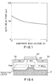
- Fig. 6 shows the semiconductor substrate in the vicinity of the gate electrode 50.
- the depth X pw of the shallow P well 11 from the surface of the substrate must be smaller than an addition of the depletion width W d just under the gate oxide film 40 and the depletion width W pw between the P well 11 (at the portion extending to the shallower side) and the N well 12; that is, X pw ⁇ W d + W pw .
- the depletion layer width W d just under the gate is dependent upon the impurity concentration in the P well 11, as shown by the characteristics in Fig. 7.
- the impurity concentration of the P well region 11 just under the gate is 1 x 10 16 cm -3 or more, so that the depth X pw of the P well region 11 from the surface of the substrate must be 0. 5 ⁇ m or less under consideration of the margin.
- the ordinate indicates the depletion width W d ( ⁇ m) just under the gate and the abscissa indicates the impurity concentration (cm -3 ) of the P well region 11 just under the gate.
- an N type (100) silicon semiconductor substrate 10 with a specific resistance of 1 to 2 ⁇ -cm is oxidized within an oxidizing atmosphere at about 1000 °C to form a silicon oxide film 22 with a thickness of about 15 nm on the surface of the semiconductor substrate as a protective film.
- a resist pattern 23 is formed in accordance with the well-known photo-etching method. Boron ions 24 are injected into a PMOS transistor forming region with the resist pattern 23 as a mask at an acceleration voltage of 160 KeV and at a dose of about 4 x 10 13 cm -2 , as shown in Fig. 2A.
- the substrate 10 is annealed within a nitriding atmosphere at about 1190 °C to form a P type impurity diffusion region 14 with a thickness of about 3 ⁇ m.
- This P type impurity diffusion region 14 is used as a deep P well 14.
- an N type impurity diffusion region 12 with a thickness of about 3 ⁇ m is formed adjoining to of the deep P well 14.
- This N type impurity diffusion region 12 is used as a deep N well 12.
- impurity (e.g., phosphorus) ions are injected and the injected impurity ions are thermally diffused, as shown in Fig. 2B.
- the surface of the semiconductor substrate 10 is oxidized within an oxidizing atmosphere at about 900 °C to a depth of about 500 Angstrom ( ⁇ ) to form a second silicon oxide film 26.
- a silicon nitride film (Si 3 N 4 ) 27 with a thickness of about 150 nm, for instance is deposited on the second silicon oxide film 26 in accordance with the chemical vapor deposition (CVD) technique.
- CVD chemical vapor deposition
- the silicon nitride film 26 is selectively removed in accordance with the RIE (reactive ion etching) technique to form an element isolating region (a field oxide film) 7. Further, after the resist pattern 28 has been removed, a new resist pattern (not shown) is formed, and boron ions are injected into a region under the element isolating region 7 for the NMOS forming region with the new resist pattern as a mask at an acceleration voltage of 160 KeV and at a dose of 1 x 10 13 to 1 x 10 14 cm -2 .
- RIE reactive ion etching
- the substrate is oxidized within the oxidizing atmosphere at about 1000 °C to form a silicon oxide film 7 (which becomes a field oxide film) with a thickness of about 600 nm at the element isolating region forming portion.
- boron ions injected under the element isolation region (the field oxide film 7) for the NMOS forming region and phosphorus ions injected under the element isolating region fcr the PMOS forming region are all activated, so that a P type impurity diffusion region 29 with a thickness of about 0. 2 to 2 ⁇ m and an N type impurity diffusion region 31 with a thickness of about 0. 1 ⁇ m or more can be both formed at the regions into which ions are injected.
- P type impurity diffusion region 29 and N type impurity diffusion region 31 are formed under the field oxide film 7 and used as channel stoppers of the transistors. Successively, the silicon nitride film 27 and the second silicon oxide film 26 are removed, as shown in Fig. 2D.
- the thickness of the N type impurity diffusion region 31 is smaller than that of the P type impurity diffusion region 29, so that the P type impurity diffusion region 29 can be connected with the deep P well 14 so as to be formed integral therewith.
- the thickness of the field oxide film 7 is about 0. 2 to 0. 7 ⁇ m, and 0. 3 ⁇ m in this embodiment.
- the semiconductor substrate 10 is thermally oxidized within the oxidizing atmosphere at 850 °C to form a third silicon oxide film 32 with a thickness of 10 nm on the surface of the element forming region of the semiconductor substrate 10, and further a polysilicon film with a thickness of about 300 nm is deposited thereon in accordance with the chemical vapor deposition (CVD) technique and in addition a silicide film such as tungsten silicide is deposited thereon to form a polycide.
- the silicon oxide film 32 and the polycide film are selectively etched with a resist mask (not shown) patterned by the photo-etching method in accordance with the reactive ion etching technique.
- a gate oxide film 40 is formed on the N well 12 and a polycide gate electrode 50 is formed on the gate oxide film 40.
- a gate oxide film 4 is formed on the P well 14 and a polycide gate electrode 5 is formed on the gate oxide film 4.
- the material of the gate electrodes 50 and 5 it is possible to use various materials such as polysilicon, a refractory metal such as tungsten, a laminated substance of the polysilicon and the refractory metal, silicide, etc. without being limited to only the polycide.
- the thickness of the gate electrodes 50 and 5 is about 0. 1 to 0. 4 ⁇ m.
- the substrate is annealed within an inert gas atmosphere at 850 °C for 10 min to activate the injected boron ions electrically and thereby to form the P type impurity diffusion region. Accordingly, the source/drain region 3 of the PMOS transistor can be formed in the deep P well 14, and the P type impurity diffusion region 36 can be formed in the deep N well 12, respectively.
- the above-mentioned method is a first process for manufacturing the semiconductor integrated circuit device to which no ions are injected to control the punch through.
- a second method of manufacturing the semiconductor integrated circuit device formed with a layer for controlling the punch through will be described hereinbelow.
- the semiconductor substrate 10 is thermally oxidized within the oxidizing atmosphere at 850 °C to form a third silicon oxide film 32 with a thickness of 10 nm on the surface of the element forming regions of the semiconductor substrate 10, and further a polysilicon film with a thickness of about 300 nm is deposited thereon in accordance with the chemical vapor deposition (CVD) technique and in addition a silicide film such as tungsten silicide is deposited thereon to form a polycide.
- the silicon oxide film 32 and the polycide film are selectively etched with a resist mask (not shown) patterned by the photo-etching method in accordance with the reactive ion etching technique.
- a gate oxide film 40 is formed on the N well 12 and a polycide gate electrode 50 is formed on the gate oxide film 40.
- a gate oxide film 4 is formed on the P well 14 and a polycide gate electrode 5 is formed on the gate oxide film 4.
- the material of the gate electrodes 5 and 50 it is possible to use various materials such as polysilicon, a refractory metal such as tungsten, a laminated substance of the polysilicon and the refractory metal, silicide, etc. without being limited to only the polycide.
- the thickness of the gate electrodes 5 and 50 is about 0. 1 to 0. 4 ⁇ m.
- boron and phosphorus ions injected are activated electrically, to form a shallow P well 34 with a depth of about 0. 4 ⁇ m from the surface of the semiconductor substrate under the gate electrode 40 within the deep N well 12, and further a shallow N well 35 with a depth of about 0. 4 ⁇ m from the surface of the semiconductor substrate under the gate electrode 4 within the deep N well 14.
- the substrate is thermally oxidized within an oxidizing atmosphere at 900 °C to form a silicon oxide film with a thickness of 10 nm on the surface of the substrate.
- boron ions are injected into the source/drain region of the NMOS transistor with the use of a mask formed by the photo-etching method at an acceleration voltage of 100 to 200 KeV and at a dose of 2 x 10 12 to 1. 5 x 10 13 cm -2 .
- phosphorus ions are injected into the source/drain region of the PMOS transistor at an acceleration voltage of 80 to 180 KeV and at a dose of 2 x 10 12 to 1. 5 x 10 13 cm -2 to form the P type impurity diffusion region 38 and the N type impurity diffusion region 39, respectively, as shown in Fig. 2E.
- These P type impurity diffusion region 38 and the N type impurity diffusion region 39 can suppress the punch through between the source/drain region and the semiconductor substrate and between the source/drain region and the first N type impurity diffusion region.
- arsenic ions are injected into the source/drain region of the NMOS transistor and the portion at which the high concentration impurity diffusion region is to be formed to obtain a well potential of the PMOS region with a resist pattern formed by the photo-etching method at an acceleration voltage of 50 KeV and at a dose of about 5 x 10 15 cm -2 .
- the substrate is annealed within an inert gas atmosphere at 850 °C for 10 min to activate the injected arsenic ions electrically and thereby to form the N type impurity diffusion region. Accordingly, the source/drain region 30 of the NMOS transistor can be formed in the deep N well 12, and the N type impurity diffusion region 37 can be formed in the deep P well 14, respectively.
- difluoroboron ions are injected into the source/drain region of the PMOS transistor and the portion at which the high concentration impurity diffusion region is to be formed to obtain a well potential of the NMOS region with a resist pattern formed by the photo-etching method at an acceleration voltage of 40 KeV and at a dose of about 3 x 10 15 cm -2 .
- the substrate is annealed within an inert gas atmosphere at 850 °C for 10 min to activate the injected boron ions electrically and thereby to form the P type impurity diffusion region. Accordingly, the source/drain region 3 of the PMOS transistor can be formed in the deep P well 14, and the P type impurity diffusion region 36 can be formed in the deep N well 12, respectively.
- the shallow P well 34, the P type impurity diffusion regions 36 and 38, and the P type impurity diffusion region 29 as shown in Fig. 2E are integrated as the shallow P well (the first well region) 11 as shown in Fig. 1. Further, the first well region is formed integral with the fourth well region (the deep N well) 14 so as to form a single region substantially.
- the shallow N well 35, the N type impurity diffusion regions 37 and 39, and the N type impurity diffusion region 31 as shown in Fig. 2E are integrated as the shallow N well (the third well region) 13 as shown in Fig. 1.
- the shallow P well 34 formed in the P type impurity diffusion region 36 becomes the P type high concentration contact region 16 in the first well region 11
- the shallow N well 35 formed in the N type impurity diffusion region 37 becomes the N type high concentration contact region 15 in the third well region 13.
- the semiconductor integrated circuit device of CMOS structure can be completed by the well-known process by forming interlayer insulating films, lead electrodes, a passivation film, etc.
- an oxide film formed in accordance with the LOCOS (localized oxidation of silicon) technique is adopted as the element isolation region.
- the other conventional element isolation structure for instance such as element isolation regions of trench structure can be applied to the integrated circuit device of the present invention.
- the impurity diffusion region at which the shallow well is to be formed
- the N type silicon semiconductor substrate with a specific resistance of 1 to 2 ⁇ cm has been adopted, it is of course possible to use an N type semiconductor substrate formed with an N type or a P type epitaxial growth layer or a P type semiconductor substrate formed with an N type or a P type epitaxial growth layer.
- the structure is characterized in that: the first region 11 and the fourth region 14 are connected to each other so as to constitute one region; the first region (the shallow P well) 11 is formed in the second region (the deep N well) 12 and the third region (the shallow N well) 13 is formed in the fourth region (the deep P well) 14 being adjoining to the second region 12; and the two P type and N type impurity diffusion regions 29 and 31 (shown in Fig. 2D) both formed at the interface region between the second and fourth regions 12 and 14 are different from each other in depth from the surface of the semiconductor substrate.
- the structure of the present invention can be achieved by the presence of this depth difference between the two adjoining impurity diffusion regions 29 and 31. These two adjoining impurity diffusion regions 29 and 31 are both formed under the field oxide film 7 as a channel stopper region. The difference in depth between the two is preferably 0. 1 to 0. 5 ⁇ m.
- the element isolation regions are formed by an oxide film formed in accordance with the LOCOS (localized oxidation of silicon) technique. Without being limited thereto, however, the same structure can be obtained when buried element isolation regions are adopted.
- LOCOS localized oxidation of silicon
- Figs. 3 and 4 show the characteristics of the MOS FET formed with the shallow well according to the present invention, in comparison with those of the conventional MOS FET formed with no shallow well.
- dashed lines indicate those of the conventional MOS FET without shallow well and the solid lines indicate those of the MOS FET formed with the shallow well of about 0. 5 ⁇ m or less from the surface of the semiconductor substrate according to the present invention.
- Fig. 3 is a graph showing the drain current and drain voltage (I d - V d ) characteristics, in which the drain voltage V d is taken on the abscissa; the drain current I d is taken on the ordinate; and the gate voltages (V g ) of - 0.
- Fig. 3 indicates that the drain current of the MOS FET formed with the shallow well of the present invention increases in comparison with the conventional MOS FET with no shallow well. Further, the threshold voltage of the MOS FET of the present invention is about 0. 5 V, which is lower than that of the conventional MOS FET of about 1. 0 V.
- Fig. 4 is a graph showing the sub-threshold current characteristics, in which the drain current ( ⁇ A) is taken on the ordinate and the gate voltage (V) is taken on the abscissa.
- Fig. 4 indicates that the sub-threshold coefficient of the MOSFET formed with the shallow well can be improved in comparison with the conventional MOS FET formed with no shallow well. In other words, even if the threshold voltage is reduced, since the leak current at zero bias voltage can be suppressed, it is possible to determine the threshold voltage to be low.
Landscapes
- Metal-Oxide And Bipolar Metal-Oxide Semiconductor Integrated Circuits (AREA)
Claims (5)
- Eine integrierte Halbleiterschaltungsvorrichtung, umfassend:ein Halbleitersubstrat (10) mit einem ersten Leitfähigkeitstyp;einen ersten Wannenbereich (11) mit einem zweiten Leitfähigkeitstyp, ausgebildet auf einem zweiten Wannenbereich (12) mit dem ersten Leitfähigkeitstyp, gebildet auf dem Halbleitersubstrat;einen dritten Wannenbereich (13) mit dem ersten Leitfähigkeitstyp, gebildet in einem vierten Wannenbereich (14) mit dem zweiten Leitfähigkeitstyp, gebildet auf dem Halbleitersubstrat, wobei der vierte Wannenbereich (14) elektrisch mit dem ersten Wannenbereich (11) durch Kontaktierung verbunden ist;Feldoxidisolierungsfilme (7), bereitgestellt auf der Oberfläche des ersten und dritten Wannenbereichs (11, 13), und die Aktivierungsbereiche der Vorrichtung umschließen;einen ersten MOS Feldeffekttransistor (30, 40, 50) mit dem ersten Leitfähigkeitstyp, gebildet in dem ersten Wannenbereich (11) und mit einer ersten Gateelektrode (50), gebildet auf einem ersten Gateisolierungsfilm (40);einen zweiten MOS Feldeffekttransistor (3, 4, 5) mit dem zweiten Leitfähigkeitstyp, gebildet in dem dritten Wannenbereich (13) und mit einer zweiten Gateelektrode (5), gebildet auf einem zweiten Gateisolierungsfilm (4);eine Einrichtung 15, 16, gebildet auf dem ersten bzw. dritten Wannenbereich (11, 13) zum Anlegen einer Vorspannung;wobei die Tiefe des ersten Wannenbereichs (11) unter der ersten Gateelektrode (50) des ersten MOS Feldeffekttransistors von dem Gateisolierungsfilm (40) gleich oder geringer als 0,5 µm ist;wobei die Tiefe des dritten Wannenbereichs (13) unter der zweiten Gateelektrode (5) des zweiten MOS Feldeffekttransistors von dem Gateisolierungsfilm (4) gleich oder geringer als 0,5 µm ist;wobei der erste Grabenbereich (11), mit einem Abschnitt gleich oder geringer als 0,5 µm an dem jeweiligen Aktivierungsbereich, der umfasst ist durch die Feldoxidisolierungsfilme (7), einen tieferen Abschnitt als der Kanalstopper unter dem Feldoxidisolierungsfilmen (7) aufweist; undwobei der dritte Wannenbereich (13), mit einem Abschnitt gleich oder geringer als 0,5 µm an dem jeweiligen Aktivierungsbereich, umfasst durch die Feldoxidisolierungsfilme (7), einen tieferen Abschnitt als der Kanalstopper unter dem Feldoxidisolierungsfilmen (7) aufweist.
- Die integrierte Halbleiterschaltungsvorrichtung nach Anspruch 1, wobei ein Feldoxidfilm (7) für Isolierungselemente im ersten Wannenbereich (11) und über dem Halbleitersubstrat ausgebildet ist; ein Kanalstopperbereich mit dem zweiten Leitfähigkeitstyp in dem ersten Wannenbereich (11) und unter dem Feldoxidfilm (7) ausgebildet ist; wobei der Kanalstopperbereich mit dem vierten Wannenbereich (14) mittels einer Kontaktierung verbunden ist.
- Die integrierte Halbleiterschaltungsvorrichtung nach Anspruch 2, wobei in dem dritten Wannenbereich ein Kanalstopperbereich mit dem ersten Leitfähigkeitstyp (13) ausgebildet ist, angrenzend an den in dem ersten Wannenbereich (11) ausgebildeten Kanalstopperbereich; und eine Tiefe, von der Oberfläche des Halbleitersubstrates, des in dem dritten Wannenbereich (13) ausgebildeten Kanalstopperbereichs niedriger als eine Tiefe, von der Oberfläche des Halbleitersubstrates, des in dem ersten Wannenbereich (11) ausgebildeten Kanalstopperbereichs ist.
- Ein Verfahren zum Herstellen einer integrierten Halbleiterschaltung, umfassend die Schritte:dadurch gekennzeichnet, dassBilden eines zweiten Wannenbereichs (12) mit einem ersten Leitfähigkeitstyp auf einem Halbleitersubstrat (10) mit dem ersten Leitfähigkeitstyp, in einem Bereich, in dem ein erster MOS Transistor auszubilden ist;Bilden eines vierten Wannenbereichs (14) mit einem zweiten Leitfähigkeitstyp auf dem Halbleitersubstrat (10), angrenzend an den zweiten Wannenbereich (12), und wo ein zweiter MOS Transistor auszubilden ist;Bilden eines ersten Wannenbereichs (11) mit dem zweiten Leitfähigkeitstyp in einem Bereich in dem zweiten Wannenbereich (12), wo ein Source, ein Drain und ein Kanal des ersten MOS Feldeffekttransistors auszubilden ist;Bilden eines dritten Wannenbereichs (13) mit dem ersten Leitfähigkeitstyp in einem Bereich in dem vierten Wannenbereich (14), in dem ein Source, ein Drain und ein Kanal des zweiten MOS Feldeffekttransistors auszubilden ist;Bilden eines ersten MOS Feldeffekttransistors (30, 40, 50) mit dem ersten Leitfähigkeitstyp in dem ersten Wannenbereich (11) und mit einer ersten Gateelektrode (50), gebildet auf einem ersten Gateisolierungsfilm (5); undBilden eines zweiten MOS Feldeffekttransistors (3, 4, 5) mit dem zweiten Leitfähigkeitstyp in dem dritten Wannenbereich (13) und mit einer zweiten Gateelektrode (5), auf einem zweiten Gateisolierungsfilm (4) ausgebildet;Bilden von Isolierungsfilmen auf der Oberfläche des ersten (11) und des dritten (13) Wannenbereichs;Ausbilden einer Einrichtung (15, 16) zum Anlegen von Vorspannungen an den ersten (11) bzw. dritten (13) Wannenbereich;Festlegen einer Tiefe des ersten Wannenbereichs unter der ersten Gateelektrode des ersten MOS Feldeffekttransistors von einer Oberfläche des Halbleitersubstrates, sodass eine Verarmungsschicht, die sich von einer Schnittstelle zwischen dem ersten Gateisolierungsfilm und dem ersten Wannenbereich in Reaktion auf eine angelegte Gatespannung an die erste Gateelektrode, mit einer Verarmungsschicht, gebildet an einer Schnittstelle zwischen dem ersten Wannenbereich und dem zweiten Wannenbereich, verbunden werden kann, und Festlegen einer Tiefe des dritten Wannenbereichs unter der zweiten Gateelektrode des zweiten MOS Feldeffekttransistors von der Oberfläche des Halbleitersubstrates, sodass eine Verarmungsschicht, die sich von einer Schnittstelle zwischen dem zweiten Gateisolierungsfilm und dem dritten Wannenbereich erstreckt, in Reaktion auf eine an die zweite Gateelektrode angelegte Gatespannung, mit einer Verarmungsschicht, gebildet an einer Schnittstelle zwischen dem dritten Wannenbereich und dem vierten Wannenbereich, verbunden werden kann;
das Verfahren weiter die Schritte umfasst:elektrisches Verbinden des vierten Wannenbereichs (14) mit dem ersten Wannenbereich (11) mittels einer Kontaktierung;Bilden des dritten Wannenbereichs, sodass dieser an einem ersten Elementbildungsbereich einen flacheren Teil, durch die Isolierungsfilme definiert, und einen tieferen Bereich als ein Kanalstopper unter den Isolierfilmen aufweist; und Bilden des ersten Wannenbereichs (11), sodass dieser an einem zweiten Elementbildungsbereich einen flacheren Teil, durch die Isolierungsfilme definiert, und einen tieferen Bereich als ein Kanalstopper unter den Isolierfilmen aufweist; undBilden des zweiten Wannenbereichs (12) des ersten Leitfähigkeitstyps, sodass er die Seiten und eine untere Oberfläche des ersten Wannenbereichs (11) umfasst. - Ein Verfahren zum Ansteuern einer integrierten Halbleiterschaltungsvorrichtung nach Anspruch 1, wobei Drainströme des ersten und zweiten MOS Feldeffekttransistors gesteuert sind durch ein Ändern einer Größe der an die Einrichtung (15, 16) zum Anlegen einer Vorspannung angelegten Vorspannung.
Applications Claiming Priority (3)
| Application Number | Priority Date | Filing Date | Title |
|---|---|---|---|
| JP23537292 | 1992-08-11 | ||
| JP23537292 | 1992-08-11 | ||
| JP235372/92 | 1992-08-11 |
Publications (3)
| Publication Number | Publication Date |
|---|---|
| EP0583008A2 EP0583008A2 (de) | 1994-02-16 |
| EP0583008A3 EP0583008A3 (en) | 1994-08-24 |
| EP0583008B1 true EP0583008B1 (de) | 2003-07-16 |
Family
ID=16985115
Family Applications (1)
| Application Number | Title | Priority Date | Filing Date |
|---|---|---|---|
| EP93112884A Expired - Lifetime EP0583008B1 (de) | 1992-08-11 | 1993-08-11 | Integriertes Halbleiterschaltkreisbauelement und dessen Herstellungsverfahren |
Country Status (4)
| Country | Link |
|---|---|
| US (1) | US5489795A (de) |
| EP (1) | EP0583008B1 (de) |
| KR (1) | KR0139773B1 (de) |
| DE (1) | DE69333098T2 (de) |
Families Citing this family (9)
| Publication number | Priority date | Publication date | Assignee | Title |
|---|---|---|---|---|
| JP3367776B2 (ja) * | 1993-12-27 | 2003-01-20 | 株式会社東芝 | 半導体装置 |
| JPH07312423A (ja) * | 1994-05-17 | 1995-11-28 | Hitachi Ltd | Mis型半導体装置 |
| US5731619A (en) * | 1996-05-22 | 1998-03-24 | International Business Machines Corporation | CMOS structure with FETS having isolated wells with merged depletions and methods of making same |
| US6163053A (en) * | 1996-11-06 | 2000-12-19 | Ricoh Company, Ltd. | Semiconductor device having opposite-polarity region under channel |
| KR20000045294A (ko) * | 1998-12-30 | 2000-07-15 | 김영환 | Cmos소자의 제조방법 |
| US6605843B1 (en) * | 2000-08-11 | 2003-08-12 | Advanced Micro Devices, Inc. | Fully depleted SOI device with tungsten damascene contacts and method of forming same |
| US6586817B1 (en) | 2001-05-18 | 2003-07-01 | Sun Microsystems, Inc. | Device including a resistive path to introduce an equivalent RC circuit |
| US6583001B1 (en) * | 2001-05-18 | 2003-06-24 | Sun Microsystems, Inc. | Method for introducing an equivalent RC circuit in a MOS device using resistive paths |
| CN116153934B (zh) * | 2023-04-20 | 2023-06-27 | 长鑫存储技术有限公司 | 半导体结构及其制备方法 |
Citations (1)
| Publication number | Priority date | Publication date | Assignee | Title |
|---|---|---|---|---|
| JPH0635558A (ja) * | 1992-07-15 | 1994-02-10 | Sharp Corp | 定電流源回路 |
Family Cites Families (3)
| Publication number | Priority date | Publication date | Assignee | Title |
|---|---|---|---|---|
| IT1214615B (it) * | 1985-06-19 | 1990-01-18 | Ates Componenti Elettron | Transistore mos a canale n con limitazione dell'effetto di perforazione (punch-through) erelativo processo di formazione. |
| JPH06105774B2 (ja) * | 1987-11-17 | 1994-12-21 | 富士通株式会社 | 半導体記憶装置及びその製造方法 |
| JPH03198282A (ja) * | 1989-12-26 | 1991-08-29 | Ricoh Co Ltd | Fifo回路 |
-
1993
- 1993-08-09 KR KR1019930015386A patent/KR0139773B1/ko not_active Expired - Fee Related
- 1993-08-11 DE DE69333098T patent/DE69333098T2/de not_active Expired - Fee Related
- 1993-08-11 EP EP93112884A patent/EP0583008B1/de not_active Expired - Lifetime
-
1994
- 1994-10-04 US US08/317,835 patent/US5489795A/en not_active Expired - Lifetime
Patent Citations (1)
| Publication number | Priority date | Publication date | Assignee | Title |
|---|---|---|---|---|
| JPH0635558A (ja) * | 1992-07-15 | 1994-02-10 | Sharp Corp | 定電流源回路 |
Non-Patent Citations (1)
| Title |
|---|
| IEEE JOURNAL OF SOLID STATE CIRCUITS, 24 (1989), S.FUJII ET AL, PAGES 1170-1175 * |
Also Published As
| Publication number | Publication date |
|---|---|
| KR0139773B1 (ko) | 1998-06-01 |
| DE69333098T2 (de) | 2004-03-25 |
| EP0583008A2 (de) | 1994-02-16 |
| DE69333098D1 (de) | 2003-08-21 |
| EP0583008A3 (en) | 1994-08-24 |
| US5489795A (en) | 1996-02-06 |
| KR940004807A (ko) | 1994-03-16 |
Similar Documents
| Publication | Publication Date | Title |
|---|---|---|
| EP0749165B1 (de) | Dünnfilmtransistor über einem isolierten Halbleitersubstrat und Verfahren zur Herstellung | |
| CN100524783C (zh) | 一种半导体结构及其制造方法 | |
| US6051509A (en) | Semiconductor integrated circuit manufacturing method and device | |
| US6255152B1 (en) | Method of fabricating CMOS using Si-B layer to form source/drain extension junction | |
| US6163053A (en) | Semiconductor device having opposite-polarity region under channel | |
| EP0166167B1 (de) | Verfahren zur Herstellung einer Halbleiteranordnung mit p-Kanal und n-Kanal MISFETs | |
| US5294822A (en) | Polycide local interconnect method and structure | |
| US6545318B1 (en) | Semiconductor device and manufacturing method thereof | |
| JPH0536918A (ja) | 半導体集積回路装置 | |
| KR19990088443A (ko) | Soi반도체장치및그제조방법 | |
| US5614432A (en) | Method for manufacturing LDD type MIS device | |
| US6605843B1 (en) | Fully depleted SOI device with tungsten damascene contacts and method of forming same | |
| JP2001156290A (ja) | 半導体装置 | |
| EP0583008B1 (de) | Integriertes Halbleiterschaltkreisbauelement und dessen Herstellungsverfahren | |
| US6586296B1 (en) | Method of doping wells, channels, and gates of dual gate CMOS technology with reduced number of masks | |
| US6110818A (en) | Semiconductor device with gate electrodes for sub-micron applications and fabrication thereof | |
| JPH08186179A (ja) | 相補型半導体装置 | |
| US6667206B2 (en) | Method of manufacturing semiconductor device | |
| KR100344489B1 (ko) | 반도체집적회로장치의제조방법 | |
| JP3425043B2 (ja) | Mis型半導体装置の製造方法 | |
| JP2845186B2 (ja) | 半導体装置とその製造方法 | |
| KR100342804B1 (ko) | 반도체 장치 및 그 제조 방법 | |
| US5691564A (en) | Semiconductor device with high speed operation and high integration | |
| US6882013B2 (en) | Transistor with reduced short channel effects and method | |
| JP2953915B2 (ja) | 半導体集積回路装置及びその製造方法 |
Legal Events
| Date | Code | Title | Description |
|---|---|---|---|
| PUAI | Public reference made under article 153(3) epc to a published international application that has entered the european phase |
Free format text: ORIGINAL CODE: 0009012 |
|
| 17P | Request for examination filed |
Effective date: 19930811 |
|
| AK | Designated contracting states |
Kind code of ref document: A2 Designated state(s): DE FR GB |
|
| PUAL | Search report despatched |
Free format text: ORIGINAL CODE: 0009013 |
|
| AK | Designated contracting states |
Kind code of ref document: A3 Designated state(s): DE FR GB |
|
| 17Q | First examination report despatched |
Effective date: 19941021 |
|
| APAB | Appeal dossier modified |
Free format text: ORIGINAL CODE: EPIDOS NOAPE |
|
| APAB | Appeal dossier modified |
Free format text: ORIGINAL CODE: EPIDOS NOAPE |
|
| APAD | Appeal reference recorded |
Free format text: ORIGINAL CODE: EPIDOS REFNE |
|
| APAD | Appeal reference recorded |
Free format text: ORIGINAL CODE: EPIDOS REFNE |
|
| APAB | Appeal dossier modified |
Free format text: ORIGINAL CODE: EPIDOS NOAPE |
|
| GRAG | Despatch of communication of intention to grant |
Free format text: ORIGINAL CODE: EPIDOS AGRA |
|
| GRAH | Despatch of communication of intention to grant a patent |
Free format text: ORIGINAL CODE: EPIDOS IGRA |
|
| GRAG | Despatch of communication of intention to grant |
Free format text: ORIGINAL CODE: EPIDOS AGRA |
|
| GRAH | Despatch of communication of intention to grant a patent |
Free format text: ORIGINAL CODE: EPIDOS IGRA |
|
| GRAH | Despatch of communication of intention to grant a patent |
Free format text: ORIGINAL CODE: EPIDOS IGRA |
|
| GRAA | (expected) grant |
Free format text: ORIGINAL CODE: 0009210 |
|
| AK | Designated contracting states |
Designated state(s): DE FR GB |
|
| REG | Reference to a national code |
Ref country code: GB Ref legal event code: FG4D |
|
| REF | Corresponds to: |
Ref document number: 69333098 Country of ref document: DE Date of ref document: 20030821 Kind code of ref document: P |
|
| ET | Fr: translation filed | ||
| PLBE | No opposition filed within time limit |
Free format text: ORIGINAL CODE: 0009261 |
|
| 26N | No opposition filed |
Effective date: 20040419 |
|
| APAH | Appeal reference modified |
Free format text: ORIGINAL CODE: EPIDOSCREFNO |
|
| PGFP | Annual fee paid to national office [announced via postgrant information from national office to epo] |
Ref country code: DE Payment date: 20080821 Year of fee payment: 16 |
|
| PGFP | Annual fee paid to national office [announced via postgrant information from national office to epo] |
Ref country code: FR Payment date: 20080818 Year of fee payment: 16 |
|
| PGFP | Annual fee paid to national office [announced via postgrant information from national office to epo] |
Ref country code: GB Payment date: 20080820 Year of fee payment: 16 |
|
| GBPC | Gb: european patent ceased through non-payment of renewal fee |
Effective date: 20090811 |
|
| REG | Reference to a national code |
Ref country code: FR Ref legal event code: ST Effective date: 20100430 |
|
| PG25 | Lapsed in a contracting state [announced via postgrant information from national office to epo] |
Ref country code: FR Free format text: LAPSE BECAUSE OF NON-PAYMENT OF DUE FEES Effective date: 20090831 Ref country code: DE Free format text: LAPSE BECAUSE OF NON-PAYMENT OF DUE FEES Effective date: 20100302 |
|
| PG25 | Lapsed in a contracting state [announced via postgrant information from national office to epo] |
Ref country code: GB Free format text: LAPSE BECAUSE OF NON-PAYMENT OF DUE FEES Effective date: 20090811 |