EP0603101A1 - Entkopplungskondensator-Struktur mit Selbstschutz - Google Patents
Entkopplungskondensator-Struktur mit Selbstschutz Download PDFInfo
- Publication number
- EP0603101A1 EP0603101A1 EP93480188A EP93480188A EP0603101A1 EP 0603101 A1 EP0603101 A1 EP 0603101A1 EP 93480188 A EP93480188 A EP 93480188A EP 93480188 A EP93480188 A EP 93480188A EP 0603101 A1 EP0603101 A1 EP 0603101A1
- Authority
- EP
- European Patent Office
- Prior art keywords
- decoupling capacitor
- integrated circuit
- capacitor
- microns
- circuit decoupling
- Prior art date
- Legal status (The legal status is an assumption and is not a legal conclusion. Google has not performed a legal analysis and makes no representation as to the accuracy of the status listed.)
- Ceased
Links
- 239000003990 capacitor Substances 0.000 title claims abstract description 52
- 230000001681 protective effect Effects 0.000 title 1
- 239000003870 refractory metal Substances 0.000 claims description 11
- 239000000758 substrate Substances 0.000 claims description 8
- 239000004065 semiconductor Substances 0.000 claims description 6
- 229910021332 silicide Inorganic materials 0.000 claims description 6
- FVBUAEGBCNSCDD-UHFFFAOYSA-N silicide(4-) Chemical compound [Si-4] FVBUAEGBCNSCDD-UHFFFAOYSA-N 0.000 claims description 6
- 229910021341 titanium silicide Inorganic materials 0.000 claims description 5
- 230000008878 coupling Effects 0.000 claims 1
- 238000010168 coupling process Methods 0.000 claims 1
- 238000005859 coupling reaction Methods 0.000 claims 1
- 238000000034 method Methods 0.000 description 11
- 150000004767 nitrides Chemical class 0.000 description 6
- 239000010936 titanium Substances 0.000 description 5
- RTAQQCXQSZGOHL-UHFFFAOYSA-N Titanium Chemical compound [Ti] RTAQQCXQSZGOHL-UHFFFAOYSA-N 0.000 description 4
- 238000004519 manufacturing process Methods 0.000 description 4
- 229910021420 polycrystalline silicon Inorganic materials 0.000 description 4
- 229920005591 polysilicon Polymers 0.000 description 4
- 229910052719 titanium Inorganic materials 0.000 description 4
- 238000002955 isolation Methods 0.000 description 3
- XUIMIQQOPSSXEZ-UHFFFAOYSA-N Silicon Chemical compound [Si] XUIMIQQOPSSXEZ-UHFFFAOYSA-N 0.000 description 2
- 230000007547 defect Effects 0.000 description 2
- 238000000151 deposition Methods 0.000 description 2
- 238000010586 diagram Methods 0.000 description 2
- 229910052710 silicon Inorganic materials 0.000 description 2
- 239000010703 silicon Substances 0.000 description 2
- VYZAMTAEIAYCRO-UHFFFAOYSA-N Chromium Chemical compound [Cr] VYZAMTAEIAYCRO-UHFFFAOYSA-N 0.000 description 1
- VYPSYNLAJGMNEJ-UHFFFAOYSA-N Silicium dioxide Chemical compound O=[Si]=O VYPSYNLAJGMNEJ-UHFFFAOYSA-N 0.000 description 1
- 229910052804 chromium Inorganic materials 0.000 description 1
- 239000011651 chromium Substances 0.000 description 1
- 239000010941 cobalt Substances 0.000 description 1
- 229910017052 cobalt Inorganic materials 0.000 description 1
- GUTLYIVDDKVIGB-UHFFFAOYSA-N cobalt atom Chemical compound [Co] GUTLYIVDDKVIGB-UHFFFAOYSA-N 0.000 description 1
- 239000002131 composite material Substances 0.000 description 1
- 238000010276 construction Methods 0.000 description 1
- 230000008021 deposition Effects 0.000 description 1
- 238000005516 engineering process Methods 0.000 description 1
- 238000005530 etching Methods 0.000 description 1
- 238000010438 heat treatment Methods 0.000 description 1
- 239000012212 insulator Substances 0.000 description 1
- 239000000463 material Substances 0.000 description 1
- 238000000206 photolithography Methods 0.000 description 1
- 229910052814 silicon oxide Inorganic materials 0.000 description 1
- 230000001052 transient effect Effects 0.000 description 1
- WFKWXMTUELFFGS-UHFFFAOYSA-N tungsten Chemical compound [W] WFKWXMTUELFFGS-UHFFFAOYSA-N 0.000 description 1
- 229910052721 tungsten Inorganic materials 0.000 description 1
- 239000010937 tungsten Substances 0.000 description 1
Images


Classifications
-
- H—ELECTRICITY
- H10—SEMICONDUCTOR DEVICES; ELECTRIC SOLID-STATE DEVICES NOT OTHERWISE PROVIDED FOR
- H10D—INORGANIC ELECTRIC SEMICONDUCTOR DEVICES
- H10D84/00—Integrated devices formed in or on semiconductor substrates that comprise only semiconducting layers, e.g. on Si wafers or on GaAs-on-Si wafers
- H10D84/201—Integrated devices formed in or on semiconductor substrates that comprise only semiconducting layers, e.g. on Si wafers or on GaAs-on-Si wafers characterised by the integration of only components covered by H10D1/00 or H10D8/00, e.g. RLC circuits
- H10D84/204—Integrated devices formed in or on semiconductor substrates that comprise only semiconducting layers, e.g. on Si wafers or on GaAs-on-Si wafers characterised by the integration of only components covered by H10D1/00 or H10D8/00, e.g. RLC circuits of combinations of diodes or capacitors or resistors
- H10D84/212—Integrated devices formed in or on semiconductor substrates that comprise only semiconducting layers, e.g. on Si wafers or on GaAs-on-Si wafers characterised by the integration of only components covered by H10D1/00 or H10D8/00, e.g. RLC circuits of combinations of diodes or capacitors or resistors of only capacitors
-
- H—ELECTRICITY
- H10—SEMICONDUCTOR DEVICES; ELECTRIC SOLID-STATE DEVICES NOT OTHERWISE PROVIDED FOR
- H10D—INORGANIC ELECTRIC SEMICONDUCTOR DEVICES
- H10D89/00—Aspects of integrated devices not covered by groups H10D84/00 - H10D88/00
- H10D89/211—Design considerations for internal polarisation
- H10D89/213—Design considerations for internal polarisation in field-effect devices
Definitions
- This invention relates to an improved integrated circuit, decoupling capacitor and, more particularly, to an integrated circuit, decoupling capacitor that reduces integrated circuit chip rejection due to manufacturing defects in the decoupling capacitor.
- a decoupling capacitor In the design of logic circuits, a decoupling capacitor is generally used to isolate the logic circuit from rapid changes in the power supply voltage, so-called power supply bounce.
- the decoupling capacitor In a typical circuit design, as shown in Figure 1, the decoupling capacitor is wired directly to the power supply and can cause a failure of an entire chip if only one decoupling capacitor develops a short circuit.
- the decoupling capacitor is a composite made up of layers of thin dielectric films deposited on top of a heavily doped N+ region.
- the thickness of the dielectric films is extremely thin (e.g., 60 ⁇ oxide/100 ⁇ nitride) and the capacitor area has to be relatively large.
- defects such as a pin hole for example, in the thin, dielectric capacitor films are a common occurrence. Since, as shown in Figure 1, the decoupling capacitor is connected directly to the power supply, a short in a single decoupling capacitor can result in a failure of the entire chip.
- An object of this invention is provision of a decoupling capacitor that is fault tolerant; a tolerance of production faults in the capacitor layers which tolerance, in turn, increases chip yield.
- Another object of this invention is provision of a fault tolerant decoupling capacitor whose construction is compatible with existing process steps and procedures for manufacturing integrated circuits.
- this invention contemplates the provision of. an integrated circuit decoupling capacitor that is divided into a plurality of discrete segments.
- the segments are connected electrically in parallel and are redundant to an extent that if one segment (or if desired more than one segment) fails, the remaining segments have sufficient capacitance to provide the required decoupling function.
- Each decoupling capacitor segment has a fuse connected in series with it. The fuse opens in response to a fault in a decoupling capacitor segment that would otherwise cause that segment to short the power supply to ground.
- Figure 1 is a schematic diagram of a prior art decoupling capacitor circuit.
- Figure 2 is a schematic diagram, similar to Figure 1, of a decoupling capacitor circuit in accordance with the teaching of this invention.
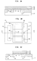
- FIGS 3A through 3F are views at various stages of one embodiment of an integrated circuit decoupling capacitor formed in accordance with the teachings of this invention.
- a typical integrated circuit has a number of logic circuits, such as logic circuits 10, formed on a semiconductor substrate 11 by a sequence of well-known process steps.
- Each logic circuit 10 is connected to an appropriate voltage source 12 also located on the semiconductor substrate.
- a decoupling capacitor 14 couples the voltage source 12 to a suitable common or "ground" terminal 16 so that any sharp fluxuations in the voltage (i.e., bounce) of source 12 are shunted through the decoupling capacitor to ground. In this manner, the decoupling capacitor 14 isolates the logic circuit 10 from rapid changes in power supply voltage.
- the circuit operation of a decoupling capacitor in accordance with the teaching of this invention is essentially the same as that described in connection with Figure 1.
- the decoupling capacitor 14 has been divided into three discrete segments, 14A, 14B and 14C.
- Three segments provide somewhat greater redundancy than two segments, provided that a single segment can perform satisfactorily the decoupling function in the event two of the other segments fail.
- four or more segments could be used, with the number chosen being a matter of design trade-off and choice.
- a current sensitive fuse link 16A, 16B and 16C is coupled respectively in series with segments 14A, 14B and 14C.
- Each fuse segment is designed so that in the event there is a short circuit across its series capacitor segment, the resultant short circuit power supply current cause the fuse link to open, disconnecting the segment from the circuit.
- the remaining segments are designed so that they have sufficient capacitance to provide the required operating decoupling function for the circuit.
- the structure may be designed so that with, for example, three discrete segments, two could fail, and the remaining segment and its fuse line would have sufficient capacitance and current carrying capacity to provide the required decoupling function in response to a power supply transient.
- a heavily doped N+ region 20 is formed in a N doped silicon substrate 21.
- a heavily doped N+ region 20 is formed in an N doped silicon substrate 21.
- the heavily doped N+ region 20 is isolated in a suitable manner by, for example, a shallow silicon oxide isolation trench 22 surrounding the region 20.
- a heavily doped N+ reach-through 26 in the isolation trench 22 provides one common contact to the decoupling capacitor segments formed on the surface of the N+ region 20.
- the decoupling capacitor segments are formed over the N+ region 20 by first depositing thin oxide layer 28 and then a thin nitride layer 30 (e.g., oxide 60 ⁇ and nitride 100 ⁇ ) using conventional prior art process steps.
- a thin nitride layer 30 e.g., oxide 60 ⁇ and nitride 100 ⁇
- the oxide layer 28 could be formed by a CVD deposition or alternatively thermally grown and the nitride may be formed by CVD deposited.
- a polysilicon layer 32 is next formed on the oxide/nitride layers 28 and 30.
- the discrete capacitor segments (14A, 14B, and 14C) and their respective fuse segments (16A, 16B, and 16C) are formed in this specific embodiment of the invention by initially etching the layers of polysilicon, nitride and oxide in desired form of segment plates 14A, 14B, and 14C joined by narrow fuse segments 16A, 16B, and 16C to a common contact region 34.
- This step in the process can be carried out using well-known photolithography technology.
- the structure at this stage is shown in Figures 3B and 3C.
- a layer of a suitable refractory metal silicide is next formed over the top surface of the patterned polysilicon layer 32.
- a layer 40 of titanium (Ti) is deposited over the entire upper surface of the patterned wafer as shown in Figure 3D.
- the structure is then annealed or heat treated to form titanium silicide (TiSi2) layer 44 in the regions where the titanium layer was in contact with the polysilicon layer 32 and in contact with the surface of the reach-through 26.
- the structure at this stage is shown in Figure 3E.
- the unreacted titanium over the trench isolation regions is etched away.
- the completed segmented capacitor structure is shown in Figure 3F.
- the capacitor segments and their fuse links could be patterned after forming a refractory metal silicide layer.
- the segmented plates and their fuse links could be made of a refractory metal (i.e., titanium; cobalt; chromium; tungsten) rather than a refractory metal silicide and the refractory metal could be formed directly on the insulator layers 28 and/or 30.
- the layer 44 is in a range between about 300 ⁇ and 500 ⁇ thick and the fuse links 16 are in a range between 0.5 microns and 3 microns wide.
- a short circuit current on the order of 10 to 15 milliamperes will cause a typical TiSi2 fuse link to open on the order of a few microseconds.
- the current causes a rapid heating of the refractory metal or refractory metal silicide and rapid electromigration causes a pulling apart of the material opening the electrical connection.
Landscapes
- Design And Manufacture Of Integrated Circuits (AREA)
- Semiconductor Integrated Circuits (AREA)
Applications Claiming Priority (2)
| Application Number | Priority Date | Filing Date | Title |
|---|---|---|---|
| US07/992,185 US5394294A (en) | 1992-12-17 | 1992-12-17 | Self protective decoupling capacitor structure |
| US992185 | 1992-12-17 |
Publications (1)
| Publication Number | Publication Date |
|---|---|
| EP0603101A1 true EP0603101A1 (de) | 1994-06-22 |
Family
ID=25538019
Family Applications (1)
| Application Number | Title | Priority Date | Filing Date |
|---|---|---|---|
| EP93480188A Ceased EP0603101A1 (de) | 1992-12-17 | 1993-11-19 | Entkopplungskondensator-Struktur mit Selbstschutz |
Country Status (3)
| Country | Link |
|---|---|
| US (1) | US5394294A (de) |
| EP (1) | EP0603101A1 (de) |
| JP (1) | JPH06283665A (de) |
Cited By (2)
| Publication number | Priority date | Publication date | Assignee | Title |
|---|---|---|---|---|
| DE19506155A1 (de) * | 1994-03-01 | 1995-09-07 | Mitsubishi Electric Corp | Halbleitervorrichtung und Verfahren zur Herstellung derselben |
| EP1416536A3 (de) * | 2002-11-04 | 2009-06-24 | Texas Instruments Incorporated | Eliminierung defekter Entkopplungskondensatoren |
Families Citing this family (23)
| Publication number | Priority date | Publication date | Assignee | Title |
|---|---|---|---|---|
| US5506457A (en) * | 1995-04-07 | 1996-04-09 | International Business Machines Corporation | Electronic switch for decoupling capacitor |
| US5770969A (en) * | 1995-08-22 | 1998-06-23 | International Business Machines Corporation | Controllable decoupling capacitor |
| US5872697A (en) * | 1996-02-13 | 1999-02-16 | International Business Machines Corporation | Integrated circuit having integral decoupling capacitor |
| US5789964A (en) * | 1997-02-14 | 1998-08-04 | International Business Machines Corporation | Decoupling capacitor network for off-state operation |
| US5896059A (en) * | 1997-05-09 | 1999-04-20 | International Business Machines Corporation | Decoupling capacitor fuse system |
| US6214694B1 (en) * | 1998-11-17 | 2001-04-10 | International Business Machines Corporation | Process of making densely patterned silicon-on-insulator (SOI) region on a wafer |
| US20010013660A1 (en) * | 1999-01-04 | 2001-08-16 | Peter Richard Duncombe | Beol decoupling capacitor |
| US6677637B2 (en) * | 1999-06-11 | 2004-01-13 | International Business Machines Corporation | Intralevel decoupling capacitor, method of manufacture and testing circuit of the same |
| US6496053B1 (en) * | 1999-10-13 | 2002-12-17 | International Business Machines Corporation | Corrosion insensitive fusible link using capacitance sensing for semiconductor devices |
| KR100464411B1 (ko) * | 2002-04-19 | 2005-01-03 | 삼성전자주식회사 | 분할된 디커플링 커패시터를 이용한 전원선 잡음 제거회로 및 이를 구비하는 반도체 장치 |
| US6631068B1 (en) | 2002-09-17 | 2003-10-07 | Parallax Power Components Llc | Segmented metallized film |
| KR100718614B1 (ko) | 2003-10-24 | 2007-05-16 | 야마하 가부시키가이샤 | 용량 소자와 퓨즈 소자를 구비한 반도체 장치 및 그 제조방법 |
| US8294505B2 (en) * | 2005-08-23 | 2012-10-23 | International Business Machines Corporation | Stackable programmable passive device and a testing method |
| US8493075B2 (en) | 2010-09-08 | 2013-07-23 | International Business Machines Corporation | Method and apparatus for preventing circuit failure |
| US8410579B2 (en) * | 2010-12-07 | 2013-04-02 | Xilinx, Inc. | Power distribution network |
| JP6097540B2 (ja) * | 2012-01-17 | 2017-03-15 | ローム株式会社 | チップコンデンサおよびその製造方法 |
| CN105103245B (zh) * | 2013-04-04 | 2019-02-19 | 罗姆股份有限公司 | 复合芯片构件、电路组件及电子设备 |
| US20140374877A1 (en) * | 2013-06-21 | 2014-12-25 | Altera Corporation | Integrated Circuits With On-Die Decoupling Capacitors |
| US9425185B2 (en) | 2014-05-29 | 2016-08-23 | Globalfoundries Inc. | Self-healing electrostatic discharge power clamp |
| KR20170030307A (ko) * | 2015-09-09 | 2017-03-17 | 삼성전자주식회사 | 분리 배치된 커패시터를 갖는 메모리 장치 |
| US12432845B2 (en) | 2020-12-25 | 2025-09-30 | Hitachi Astemo, Ltd. | Vehicle-mounted electronic control device |
| JP2023115493A (ja) * | 2022-02-08 | 2023-08-21 | 日産自動車株式会社 | コンデンサ |
| DE102023207784A1 (de) * | 2023-08-11 | 2025-02-13 | Vitesco Technologies Germany Gmbh | Elektrische Schaltung mit einer Widerstandssicherung |
Citations (2)
| Publication number | Priority date | Publication date | Assignee | Title |
|---|---|---|---|---|
| JPH01105569A (ja) * | 1987-10-19 | 1989-04-24 | Oki Electric Ind Co Ltd | 半導体集積装置及びその不良除去方法 |
| JPH0438862A (ja) * | 1990-06-04 | 1992-02-10 | Nec Corp | 半導体集積回路装置 |
Family Cites Families (17)
| Publication number | Priority date | Publication date | Assignee | Title |
|---|---|---|---|---|
| US1842374A (en) * | 1927-10-22 | 1932-01-26 | Dubilier Condenser Corp | Power factor condenser |
| US2216558A (en) * | 1937-01-19 | 1940-10-01 | Bosch Gmbh Robert | Electrostatic condenser |
| US3303400A (en) * | 1961-07-25 | 1967-02-07 | Fairchild Camera Instr Co | Semiconductor device complex |
| US3772097A (en) * | 1967-05-09 | 1973-11-13 | Motorola Inc | Epitaxial method for the fabrication of a distributed semiconductor power supply containing a decoupling capacitor |
| US3769105A (en) * | 1970-01-26 | 1973-10-30 | Ibm | Process for making an integrated circuit with a damping resistor in combination with a buried decoupling capacitor |
| US3619725A (en) * | 1970-04-08 | 1971-11-09 | Rca Corp | Electrical fuse link |
| US4553050A (en) * | 1983-12-27 | 1985-11-12 | International Business Machines Corporation | Transmission line terminator-decoupling capacitor chip for off-chip driver |
| JPS6170746A (ja) * | 1984-09-14 | 1986-04-11 | Matsushita Electronics Corp | 半導体装置 |
| FR2583221B1 (fr) * | 1985-06-07 | 1987-07-31 | Labo Electronique Physique | Dispositif semiconducteur pour la realisation des capacites de decouplage placees entre l'alimentation et la masse des circuits integres |
| JPH0789529B2 (ja) * | 1986-02-07 | 1995-09-27 | 日本電気株式会社 | ヒューズ付き固体電解コンデンサ |
| JPS62188256A (ja) * | 1986-02-13 | 1987-08-17 | Nec Corp | 集積回路チツプ |
| GB2186752A (en) * | 1986-02-15 | 1987-08-19 | Stc Plc | Fuse for electronic component |
| US4680670A (en) * | 1986-09-29 | 1987-07-14 | Avx Corporation | Fail safe ceramic capacitor |
| US4945399A (en) * | 1986-09-30 | 1990-07-31 | International Business Machines Corporation | Electronic package with integrated distributed decoupling capacitors |
| US4894746A (en) * | 1987-06-06 | 1990-01-16 | Murata Manufacturing Co., Ltd. | Laminated capacitor with fuse function |
| US5032892A (en) * | 1988-05-31 | 1991-07-16 | Micron Technology, Inc. | Depletion mode chip decoupling capacitor |
| ES2070222T3 (es) * | 1989-09-19 | 1995-06-01 | Siemens Ag | Procedimiento para la fabricacion de un condensador de electrolito solido, ejecutado en forma de chip, con elemento de proteccion. |
-
1992
- 1992-12-17 US US07/992,185 patent/US5394294A/en not_active Expired - Lifetime
-
1993
- 1993-11-19 EP EP93480188A patent/EP0603101A1/de not_active Ceased
- 1993-12-08 JP JP5308374A patent/JPH06283665A/ja active Pending
Patent Citations (2)
| Publication number | Priority date | Publication date | Assignee | Title |
|---|---|---|---|---|
| JPH01105569A (ja) * | 1987-10-19 | 1989-04-24 | Oki Electric Ind Co Ltd | 半導体集積装置及びその不良除去方法 |
| JPH0438862A (ja) * | 1990-06-04 | 1992-02-10 | Nec Corp | 半導体集積回路装置 |
Non-Patent Citations (2)
| Title |
|---|
| PATENT ABSTRACTS OF JAPAN vol. 13, no. 346 (E - 798) 3 August 1989 (1989-08-03) * |
| PATENT ABSTRACTS OF JAPAN vol. 16, no. 224 (E - 1206) 25 February 1992 (1992-02-25) * |
Cited By (4)
| Publication number | Priority date | Publication date | Assignee | Title |
|---|---|---|---|---|
| DE19506155A1 (de) * | 1994-03-01 | 1995-09-07 | Mitsubishi Electric Corp | Halbleitervorrichtung und Verfahren zur Herstellung derselben |
| US5736776A (en) * | 1994-03-01 | 1998-04-07 | Mitsubishi Denki Kabushiki Kaisha | Semiconductor device and method of manufacturing the same |
| US6096619A (en) * | 1994-03-01 | 2000-08-01 | Mitsubishi Denki Kabushiki Kaisha | Method of manufacturing a semiconductor device comprising a capacitor with an intrinsic polysilicon electrode |
| EP1416536A3 (de) * | 2002-11-04 | 2009-06-24 | Texas Instruments Incorporated | Eliminierung defekter Entkopplungskondensatoren |
Also Published As
| Publication number | Publication date |
|---|---|
| US5394294A (en) | 1995-02-28 |
| JPH06283665A (ja) | 1994-10-07 |
Similar Documents
| Publication | Publication Date | Title |
|---|---|---|
| US5394294A (en) | Self protective decoupling capacitor structure | |
| EP0700091B1 (de) | Kompakte integrierte Kondensator-Widerstand/Induktor-Struktur | |
| US6927440B2 (en) | Metal-insulator-metal capacitor | |
| US5416356A (en) | Integrated circuit having passive circuit elements | |
| US5181096A (en) | Electrically programmable antifuse incorporating dielectric and amorphous silicon interlayer | |
| US6437385B1 (en) | Integrated circuit capacitor | |
| EP0452091B1 (de) | Elektrisch programmierbares Antischmelzsicherungselement und Verfahren zu seiner Herstellung | |
| US5578836A (en) | Electrically programmable antifuse element | |
| US5804500A (en) | Fabrication process for raised tungsten plug antifuse | |
| US5304506A (en) | On chip decoupling capacitor | |
| US5986322A (en) | Reduced leakage antifuse structure | |
| US20050139959A1 (en) | Intralevel decoupling capacitor, method of manufacture and testing circuit of the same | |
| US6362023B1 (en) | Dielectric-based anti-fuse cell with polysilicon contact plug and method for its manufacture | |
| US11276748B2 (en) | Switchable metal insulator metal capacitor | |
| GB2504032A (en) | Modularized three-dimensional capacitor array | |
| US5682059A (en) | Semiconductor device including anti-fuse element and method of manufacturing the device | |
| JP3701877B2 (ja) | キャパシタを有する集積回路 | |
| US6284619B1 (en) | Integration scheme for multilevel metallization structures | |
| US4894705A (en) | Semiconductor device | |
| WO1994007266A1 (en) | A voltage programmable link having reduced capacitance | |
| US6208009B1 (en) | RC-networks in semiconductor devices and method therefor | |
| US11101213B2 (en) | EFuse structure with multiple links | |
| WO2022177971A1 (en) | Gate metal-insulator-field plate metal integrated circuit capacitor and method of forming the same | |
| US6603142B1 (en) | Antifuse incorporating tantalum nitride barrier layer | |
| KR20000015349A (ko) | 반도체 집적회로의 커패시터 제조방법 |
Legal Events
| Date | Code | Title | Description |
|---|---|---|---|
| PUAI | Public reference made under article 153(3) epc to a published international application that has entered the european phase |
Free format text: ORIGINAL CODE: 0009012 |
|
| AK | Designated contracting states |
Kind code of ref document: A1 Designated state(s): DE FR GB |
|
| 17P | Request for examination filed |
Effective date: 19941021 |
|
| 17Q | First examination report despatched |
Effective date: 19961118 |
|
| GRAG | Despatch of communication of intention to grant |
Free format text: ORIGINAL CODE: EPIDOS AGRA |
|
| STAA | Information on the status of an ep patent application or granted ep patent |
Free format text: STATUS: THE APPLICATION HAS BEEN REFUSED |
|
| 18R | Application refused |
Effective date: 19980523 |