EP0616484A1 - Magnetoresistiver Wandler und Verfahren zu seiner Herstellung - Google Patents
Magnetoresistiver Wandler und Verfahren zu seiner Herstellung Download PDFInfo
- Publication number
- EP0616484A1 EP0616484A1 EP94400559A EP94400559A EP0616484A1 EP 0616484 A1 EP0616484 A1 EP 0616484A1 EP 94400559 A EP94400559 A EP 94400559A EP 94400559 A EP94400559 A EP 94400559A EP 0616484 A1 EP0616484 A1 EP 0616484A1
- Authority
- EP
- European Patent Office
- Prior art keywords
- layer
- layers
- particles
- transducer according
- conductive
- Prior art date
- Legal status (The legal status is an assumption and is not a legal conclusion. Google has not performed a legal analysis and makes no representation as to the accuracy of the status listed.)
- Ceased
Links
Images


Classifications
-
- H—ELECTRICITY
- H10—SEMICONDUCTOR DEVICES; ELECTRIC SOLID-STATE DEVICES NOT OTHERWISE PROVIDED FOR
- H10N—ELECTRIC SOLID-STATE DEVICES NOT OTHERWISE PROVIDED FOR
- H10N50/00—Galvanomagnetic devices
- H10N50/10—Magnetoresistive devices
-
- G—PHYSICS
- G01—MEASURING; TESTING
- G01R—MEASURING ELECTRIC VARIABLES; MEASURING MAGNETIC VARIABLES
- G01R33/00—Arrangements or instruments for measuring magnetic variables
- G01R33/02—Measuring direction or magnitude of magnetic fields or magnetic flux
- G01R33/06—Measuring direction or magnitude of magnetic fields or magnetic flux using galvano-magnetic devices
- G01R33/09—Magnetoresistive devices
-
- H—ELECTRICITY
- H04—ELECTRIC COMMUNICATION TECHNIQUE
- H04R—LOUDSPEAKERS, MICROPHONES, GRAMOPHONE PICK-UPS OR LIKE ACOUSTIC ELECTROMECHANICAL TRANSDUCERS; ELECTRIC HEARING AIDS; PUBLIC ADDRESS SYSTEMS
- H04R15/00—Magnetostrictive transducers
-
- Y—GENERAL TAGGING OF NEW TECHNOLOGICAL DEVELOPMENTS; GENERAL TAGGING OF CROSS-SECTIONAL TECHNOLOGIES SPANNING OVER SEVERAL SECTIONS OF THE IPC; TECHNICAL SUBJECTS COVERED BY FORMER USPC CROSS-REFERENCE ART COLLECTIONS [XRACs] AND DIGESTS
- Y10—TECHNICAL SUBJECTS COVERED BY FORMER USPC
- Y10T—TECHNICAL SUBJECTS COVERED BY FORMER US CLASSIFICATION
- Y10T428/00—Stock material or miscellaneous articles
- Y10T428/24—Structurally defined web or sheet [e.g., overall dimension, etc.]
- Y10T428/24802—Discontinuous or differential coating, impregnation or bond [e.g., artwork, printing, retouched photograph, etc.]
- Y10T428/24917—Discontinuous or differential coating, impregnation or bond [e.g., artwork, printing, retouched photograph, etc.] including metal layer
Definitions
- the invention relates to a magnetoresistive transducer and a method for producing such a transducer.
- MMM Magnetic Metallic Multilayers
- a type A material for example, is magnetic while a type B material is non-magnetic.
- the invention therefore relates to a method characterized in that the interruption is carried out by etching.
- the magnetoresistive transducer comprises several even and odd order interruptions, the even order interruptions interrupting the electrical conduction of one of the layers of conductive material while the odd order interruptions interrupt the electrical conduction of the other layer of conductive material.
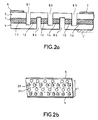
- This device comprises a layer 1 of a composite material consisting of particles of magnetic material and of particles of insulating or semiconductor material. This layer is sandwiched between two layers 4 and 5 of conductive materials.
- One of the conductive layers, for example 5, carries two electrodes 6 and 7 located at two opposite ends of the layer 5.
- the electrodes could also be one on the layer 5, the other on the layer 4.
- the electrode 7 could be at the location denoted 7 ′ in FIG. 2a.
- the layer stack comprises at least one interruption from the point of view of electrical conduction, this interruption affecting layer 1 and at least one conductive layer 4 and 5.
- a preferred practical embodiment provides for several interruptions. Odd order interruptions 8.1, 8.3, 8.5 are made in the conductive layer 5 and in layer 1. Even order interruptions 8.2, 8.4 are made in the conductive layer 4 and in layer 1. Thus a current which should circulate between the electrodes 6 and 7 will have to pass by the various elements 1.1 to 1.6.
- the structure of FIG. 2a therefore functions as if the various elements 1.1 to 1.6 had been stacked. Furthermore, the surface of the electrodes 6 and 7 can be very large, therefore its resistance low compared to that of the elements 1.2 to 1.5.
- This invention also applies to granular material. It is then possible to arrange the particles in layer 1 according to a determined distribution. In particular, according to FIG. 2b, provision is made for alternating layers of particles of different types.
- the means making it possible to apply this continuous magnetic field could be a permanent magnet such as a layer of magnetic material 16 shown in FIG. 3.
- This layer 16 can be a thin or thick layer depending on the intensity of magnetization induced and depending on the thickness of layer 1. It can be isolated from layer 4 by an insulation layer 17.
- Figure 4d we then represent the path taken by the current.
- the metallic multilayer is crossed 4 times by a current perpendicular to the plane of the deposit, but it is obvious that the number of passages can be multiplied as many times as desired.
- FIGS. 5a to 5c Another example of a method consists in carrying out the operations shown diagrammatically in FIGS. 5a to 5c.
- the first layer of conductive material 4 On a substrate 10 etched (chemically or by ion erosion) and having slots (48) of small widths (approximately 1 ⁇ m) is deposited the first layer of conductive material 4 then the layer of composite material 1. The structure of the Figure 5a. Then the second layer of conductive material 5 is deposited (FIG. 5b).
- the height of the slot h is provided greater than the thickness of the first layer of conductive material 4 increased by the thickness of the layer 1 but less than the total height of the deposit (first layer 4, layer 1, second layer 5).
- first conductive layer 4 located on the slot 48 and the second conductive layers 5 located on either side of the slot 48 which ensures electrical continuity above the slot.
- the device thus designed makes it possible to minimize the contact resistances R c of the electrodes and the access resistances R a situated between the electrodes and sensitive zones of the device with respect to the resistance of the device.
- the width e of each element of the device can be of the order of a micrometer and several elements are placed in series, which considerably increases the resistance of the device compared to the resistances R c and R a .
- the layer of composite material 1 is made up of two materials (two types of particles), but it is obvious that it is possible to provide a composite material made up of more than two types of material.
- the invention has the advantage of being able to place the transducer near a magnetic information carrier to read. For example, you can make a magnetic strip near the transducer without being bothered by the electrodes.
Landscapes
- Physics & Mathematics (AREA)
- Engineering & Computer Science (AREA)
- Acoustics & Sound (AREA)
- Signal Processing (AREA)
- Condensed Matter Physics & Semiconductors (AREA)
- General Physics & Mathematics (AREA)
- Hall/Mr Elements (AREA)
- Measuring Magnetic Variables (AREA)
Applications Claiming Priority (2)
| Application Number | Priority Date | Filing Date | Title |
|---|---|---|---|
| FR9303206A FR2702919B1 (fr) | 1993-03-19 | 1993-03-19 | Transducteur magnétorésistif et procédé de réalisation. |
| FR9303206 | 1993-03-19 |
Publications (1)
| Publication Number | Publication Date |
|---|---|
| EP0616484A1 true EP0616484A1 (de) | 1994-09-21 |
Family
ID=9445166
Family Applications (1)
| Application Number | Title | Priority Date | Filing Date |
|---|---|---|---|
| EP94400559A Ceased EP0616484A1 (de) | 1993-03-19 | 1994-03-15 | Magnetoresistiver Wandler und Verfahren zu seiner Herstellung |
Country Status (4)
| Country | Link |
|---|---|
| US (1) | US5474833A (de) |
| EP (1) | EP0616484A1 (de) |
| JP (1) | JPH077195A (de) |
| FR (1) | FR2702919B1 (de) |
Cited By (2)
| Publication number | Priority date | Publication date | Assignee | Title |
|---|---|---|---|---|
| WO1996007208A1 (en) * | 1994-08-31 | 1996-03-07 | Douwe Johannes Monsma | Current conducting structure with at least one potential barrier and method of manufcturing such |
| EP0645759A3 (de) * | 1993-09-24 | 1996-05-22 | Philips Electronics Nv | Magnetoresistive Einrichtung und eine solche Einrichtung enthaltender Magnetkopf. |
Families Citing this family (17)
| Publication number | Priority date | Publication date | Assignee | Title |
|---|---|---|---|---|
| JPH077195B2 (ja) * | 1986-08-06 | 1995-01-30 | コニカ株式会社 | ハロゲン化銀カラ−写真感光材料の処理方法 |
| US5585198A (en) * | 1993-10-20 | 1996-12-17 | Sanyo Electric Co., Ltd. | Magnetorsistance effect element |
| US5736921A (en) * | 1994-03-23 | 1998-04-07 | Sanyo Electric Co., Ltd. | Magnetoresistive element |
| SG52781A1 (en) * | 1994-02-21 | 1998-09-28 | Philips Electronics Nv | A method and a device for locally altering the magnetization direction in a body of magnetic material |
| US5695858A (en) * | 1994-03-23 | 1997-12-09 | Sanyo Electric Co., Ltd. | Magnetoresistive element |
| JP2901501B2 (ja) * | 1994-08-29 | 1999-06-07 | ティーディーケイ株式会社 | 磁性多層膜およびその製造方法ならびに磁気抵抗効果素子 |
| JPH08130337A (ja) * | 1994-09-09 | 1996-05-21 | Sanyo Electric Co Ltd | 磁気抵抗素子及びその製造方法 |
| DE69513630T2 (de) * | 1994-10-05 | 2000-06-21 | Koninklijke Philips Electronics N.V., Eindhoven | Magnetische mehrlagenanordnung, die eine doppelbarrierenstruktur mit resonantem tunneleffekt enthält |
| FR2734058B1 (fr) * | 1995-05-12 | 1997-06-20 | Thomson Csf | Amperemetre |
| US5585986A (en) * | 1995-05-15 | 1996-12-17 | International Business Machines Corporation | Digital magnetoresistive sensor based on the giant magnetoresistance effect |
| US5627704A (en) * | 1996-02-12 | 1997-05-06 | Read-Rite Corporation | Thin film giant magnetoresistive CPP transducer with flux guide yoke structure |
| EP0843827A2 (de) * | 1996-06-12 | 1998-05-27 | Koninklijke Philips Electronics N.V. | Magnetoresistiver magnetfühler |
| FR2771511B1 (fr) * | 1997-11-25 | 2000-02-04 | Thomson Csf | Capteur de champ magnetique et procede de fabrication de ce capteur |
| US6215301B1 (en) * | 1998-04-24 | 2001-04-10 | U.S. Philips Corporation | Magnetoresistive detector comprising a layer structure and a current directing means |
| JP2002523849A (ja) * | 1998-08-25 | 2002-07-30 | コーニンクレッカ フィリップス エレクトロニクス エヌ ヴィ | 薄膜シールド型磁気再生ヘッド装置 |
| US6707648B2 (en) * | 2000-05-19 | 2004-03-16 | Nih N University | Magnetic device, magnetic head and magnetic adjustment method |
| JP3958947B2 (ja) * | 2001-09-14 | 2007-08-15 | アルプス電気株式会社 | 磁気検出素子及びその製造方法 |
Citations (3)
| Publication number | Priority date | Publication date | Assignee | Title |
|---|---|---|---|---|
| EP0152000A2 (de) * | 1984-01-27 | 1985-08-21 | Hitachi, Ltd. | Magnetischer Wandler, der den Magnetwiderstandseffekt verwendet |
| EP0221540A2 (de) * | 1985-11-05 | 1987-05-13 | Sony Corporation | Den Magnetwiderstandseffekt verwendender Magnetwandlerkopf |
| EP0406060A1 (de) * | 1989-06-27 | 1991-01-02 | Thomson-Csf | Magnetwiderstandseffektwandler |
Family Cites Families (7)
| Publication number | Priority date | Publication date | Assignee | Title |
|---|---|---|---|---|
| JPS58166510A (ja) * | 1982-03-29 | 1983-10-01 | Toshiba Corp | 磁気再生装置 |
| US4800457A (en) * | 1987-09-29 | 1989-01-24 | Carnegie-Mellon University | Magnetoresistive sensor element |
| US5159513A (en) * | 1991-02-08 | 1992-10-27 | International Business Machines Corporation | Magnetoresistive sensor based on the spin valve effect |
| FR2685489B1 (fr) * | 1991-12-23 | 1994-08-05 | Thomson Csf | Capteur de champ magnetique faible a effet magnetoresistif. |
| US5373238A (en) * | 1992-11-06 | 1994-12-13 | International Business Machines Corporation | Four layer magnetoresistance device and method for making a four layer magnetoresistance device |
| US5287238A (en) * | 1992-11-06 | 1994-02-15 | International Business Machines Corporation | Dual spin valve magnetoresistive sensor |
| US5301079A (en) * | 1992-11-17 | 1994-04-05 | International Business Machines Corporation | Current biased magnetoresistive spin valve sensor |
-
1993
- 1993-03-19 FR FR9303206A patent/FR2702919B1/fr not_active Expired - Fee Related
-
1994
- 1994-03-07 US US08/206,143 patent/US5474833A/en not_active Expired - Fee Related
- 1994-03-15 EP EP94400559A patent/EP0616484A1/de not_active Ceased
- 1994-03-17 JP JP6047325A patent/JPH077195A/ja active Pending
Patent Citations (3)
| Publication number | Priority date | Publication date | Assignee | Title |
|---|---|---|---|---|
| EP0152000A2 (de) * | 1984-01-27 | 1985-08-21 | Hitachi, Ltd. | Magnetischer Wandler, der den Magnetwiderstandseffekt verwendet |
| EP0221540A2 (de) * | 1985-11-05 | 1987-05-13 | Sony Corporation | Den Magnetwiderstandseffekt verwendender Magnetwandlerkopf |
| EP0406060A1 (de) * | 1989-06-27 | 1991-01-02 | Thomson-Csf | Magnetwiderstandseffektwandler |
Cited By (2)
| Publication number | Priority date | Publication date | Assignee | Title |
|---|---|---|---|---|
| EP0645759A3 (de) * | 1993-09-24 | 1996-05-22 | Philips Electronics Nv | Magnetoresistive Einrichtung und eine solche Einrichtung enthaltender Magnetkopf. |
| WO1996007208A1 (en) * | 1994-08-31 | 1996-03-07 | Douwe Johannes Monsma | Current conducting structure with at least one potential barrier and method of manufcturing such |
Also Published As
| Publication number | Publication date |
|---|---|
| JPH077195A (ja) | 1995-01-10 |
| FR2702919A1 (fr) | 1994-09-23 |
| FR2702919B1 (fr) | 1995-05-12 |
| US5474833A (en) | 1995-12-12 |
Similar Documents
| Publication | Publication Date | Title |
|---|---|---|
| EP0616484A1 (de) | Magnetoresistiver Wandler und Verfahren zu seiner Herstellung | |
| Soulen Jr et al. | Measuring the spin polarization of a metal with a superconducting point contact | |
| EP1435101B1 (de) | Magnetoresistive hochleistungs-spinventilanordnung | |
| EP0909391A1 (de) | Dünnschicht magnetfeldsensor | |
| KR100696960B1 (ko) | 좁은 밴드갭을 갖는 이종 반도체에 있어서의 실온에서의이상 자기저항 | |
| FR2729790A1 (fr) | Magnetoresistance geante, procede de fabrication et application a un capteur magnetique | |
| WO2011092406A1 (fr) | Magnetometre integre et son procede de fabrication | |
| EP0284495B1 (de) | Magnetkopf zum Lesen von Spuren mit sehr schmaler Breite und Herstellungverfahren | |
| EP0577469B1 (de) | Magnetoresistiver Wandler | |
| EP0206865B1 (de) | Linearer Magnetoresistiver Fühler, Verfahren zu seiner Herstellung und Anwendung in einem Detektor für magnetische Gebiete | |
| EP0467736B1 (de) | Magnetoresistiver Effekt verwendender Lesemagnetkopf | |
| EP1604220A1 (de) | Magnetoresistiver wandler mit einem ferromagnetischen/antiferromagnetischen fühlelement | |
| EP0721670A1 (de) | Magnetoresistiver stromsensor und verfahren zu seiner herstellung | |
| EP0954754A1 (de) | Magnetfelddetektor und dessen herstellungsverfahren | |
| EP0642181B1 (de) | Magnetoresistive Anordnung und Fühler mit wiederholenden geometrischen Strukturen | |
| FR2709549A1 (fr) | Guide de flux magnétique à languettes et capteur magnétorésistif comportant ce guide . | |
| WO2000036429A1 (fr) | Capteur de champ magnetique a magnetoresistance geante | |
| Caruge et al. | Probing local currents in semiconductors with single molecules | |
| EP3053202B1 (de) | Verfahren zur herstellung eines josephson-übergangs und zugehöriger josephson-übergang | |
| EP2002275A1 (de) | Magnetfeldempfindliche komponente mit einem verdünnten magnetischen halbleiter, diese enthaltende anordnungen und benutzungsverfahren | |
| FR2802011A1 (fr) | Tete de lecture planaire a element magneto-resistif | |
| EP0779610A2 (de) | Aufzeichnungsvorrichtung mit Mikrospitze mit mehrschichtigem magnetoresistivem Überzug | |
| US8697562B2 (en) | Metal contacts for molecular device junctions and surface-diffusion-mediated deposition | |
| FR2463512A1 (fr) | Perfectionnements aux dispositifs a jonctions tunnel et aux procedes de fabrication de telles jonctions | |
| Gester et al. | Electron spectroscopic evidence of metastable alloy formation of Ag and Au in Co |
Legal Events
| Date | Code | Title | Description |
|---|---|---|---|
| PUAI | Public reference made under article 153(3) epc to a published international application that has entered the european phase |
Free format text: ORIGINAL CODE: 0009012 |
|
| AK | Designated contracting states |
Kind code of ref document: A1 Designated state(s): DE GB |
|
| 17P | Request for examination filed |
Effective date: 19950304 |
|
| 17Q | First examination report despatched |
Effective date: 19970312 |
|
| GRAG | Despatch of communication of intention to grant |
Free format text: ORIGINAL CODE: EPIDOS AGRA |
|
| STAA | Information on the status of an ep patent application or granted ep patent |
Free format text: STATUS: THE APPLICATION HAS BEEN REFUSED |
|
| 18R | Application refused |
Effective date: 19991216 |