EP0634500B1 - Planar magnetron sputtering apparatus - Google Patents
Planar magnetron sputtering apparatus Download PDFInfo
- Publication number
- EP0634500B1 EP0634500B1 EP94304676A EP94304676A EP0634500B1 EP 0634500 B1 EP0634500 B1 EP 0634500B1 EP 94304676 A EP94304676 A EP 94304676A EP 94304676 A EP94304676 A EP 94304676A EP 0634500 B1 EP0634500 B1 EP 0634500B1
- Authority
- EP
- European Patent Office
- Prior art keywords
- target
- magnet
- planar magnetron
- planar
- backing plate
- Prior art date
- Legal status (The legal status is an assumption and is not a legal conclusion. Google has not performed a legal analysis and makes no representation as to the accuracy of the status listed.)
- Expired - Lifetime
Links
- 238000001755 magnetron sputter deposition Methods 0.000 title description 3
- 239000002826 coolant Substances 0.000 claims description 20
- 239000000463 material Substances 0.000 claims description 11
- RYGMFSIKBFXOCR-UHFFFAOYSA-N Copper Chemical compound [Cu] RYGMFSIKBFXOCR-UHFFFAOYSA-N 0.000 claims description 5
- 229910052802 copper Inorganic materials 0.000 claims description 5
- 239000010949 copper Substances 0.000 claims description 5
- 229910001172 neodymium magnet Inorganic materials 0.000 claims description 4
- 238000004891 communication Methods 0.000 claims description 2
- RTAQQCXQSZGOHL-UHFFFAOYSA-N Titanium Chemical compound [Ti] RTAQQCXQSZGOHL-UHFFFAOYSA-N 0.000 description 14
- 230000003628 erosive effect Effects 0.000 description 14
- 239000010936 titanium Substances 0.000 description 14
- 238000004544 sputter deposition Methods 0.000 description 13
- 229910052719 titanium Inorganic materials 0.000 description 13
- 239000013077 target material Substances 0.000 description 12
- 239000000758 substrate Substances 0.000 description 11
- XKRFYHLGVUSROY-UHFFFAOYSA-N Argon Chemical compound [Ar] XKRFYHLGVUSROY-UHFFFAOYSA-N 0.000 description 6
- XLYOFNOQVPJJNP-UHFFFAOYSA-N water Substances O XLYOFNOQVPJJNP-UHFFFAOYSA-N 0.000 description 5
- 238000000151 deposition Methods 0.000 description 4
- 230000008021 deposition Effects 0.000 description 4
- 239000007789 gas Substances 0.000 description 4
- 229910001209 Low-carbon steel Inorganic materials 0.000 description 3
- 229910052786 argon Inorganic materials 0.000 description 3
- 239000000919 ceramic Substances 0.000 description 3
- 239000002131 composite material Substances 0.000 description 3
- 229910052751 metal Inorganic materials 0.000 description 3
- 239000002184 metal Substances 0.000 description 3
- 239000010935 stainless steel Substances 0.000 description 3
- 229910001220 stainless steel Inorganic materials 0.000 description 3
- PXHVJJICTQNCMI-UHFFFAOYSA-N Nickel Chemical compound [Ni] PXHVJJICTQNCMI-UHFFFAOYSA-N 0.000 description 2
- GWEVSGVZZGPLCZ-UHFFFAOYSA-N Titan oxide Chemical compound O=[Ti]=O GWEVSGVZZGPLCZ-UHFFFAOYSA-N 0.000 description 2
- 238000005219 brazing Methods 0.000 description 2
- 238000005260 corrosion Methods 0.000 description 2
- 230000007797 corrosion Effects 0.000 description 2
- 238000013461 design Methods 0.000 description 2
- 230000005684 electric field Effects 0.000 description 2
- 238000002474 experimental method Methods 0.000 description 2
- 239000011521 glass Substances 0.000 description 2
- 239000011261 inert gas Substances 0.000 description 2
- 150000002500 ions Chemical class 0.000 description 2
- 238000005259 measurement Methods 0.000 description 2
- 238000000034 method Methods 0.000 description 2
- 238000005476 soldering Methods 0.000 description 2
- 229910001200 Ferrotitanium Inorganic materials 0.000 description 1
- HCHKCACWOHOZIP-UHFFFAOYSA-N Zinc Chemical compound [Zn] HCHKCACWOHOZIP-UHFFFAOYSA-N 0.000 description 1
- 239000000853 adhesive Substances 0.000 description 1
- 230000001070 adhesive effect Effects 0.000 description 1
- 229910000828 alnico Inorganic materials 0.000 description 1
- QVGXLLKOCUKJST-UHFFFAOYSA-N atomic oxygen Chemical compound [O] QVGXLLKOCUKJST-UHFFFAOYSA-N 0.000 description 1
- 239000011248 coating agent Substances 0.000 description 1
- 238000000576 coating method Methods 0.000 description 1
- 238000001816 cooling Methods 0.000 description 1
- 238000011161 development Methods 0.000 description 1
- 230000017525 heat dissipation Effects 0.000 description 1
- AMGQUBHHOARCQH-UHFFFAOYSA-N indium;oxotin Chemical compound [In].[Sn]=O AMGQUBHHOARCQH-UHFFFAOYSA-N 0.000 description 1
- 238000009434 installation Methods 0.000 description 1
- 239000012212 insulator Substances 0.000 description 1
- 238000010849 ion bombardment Methods 0.000 description 1
- 150000002736 metal compounds Chemical class 0.000 description 1
- 150000002739 metals Chemical class 0.000 description 1
- 229910052759 nickel Inorganic materials 0.000 description 1
- 239000001301 oxygen Substances 0.000 description 1
- 229910052760 oxygen Inorganic materials 0.000 description 1
- 238000007747 plating Methods 0.000 description 1
- 238000005546 reactive sputtering Methods 0.000 description 1
- 238000007789 sealing Methods 0.000 description 1
- 239000011701 zinc Substances 0.000 description 1
- 229910052725 zinc Inorganic materials 0.000 description 1
Images


Classifications
-
- H—ELECTRICITY
- H01—ELECTRIC ELEMENTS
- H01J—ELECTRIC DISCHARGE TUBES OR DISCHARGE LAMPS
- H01J37/00—Discharge tubes with provision for introducing objects or material to be exposed to the discharge, e.g. for the purpose of examination or processing thereof
- H01J37/32—Gas-filled discharge tubes
- H01J37/34—Gas-filled discharge tubes operating with cathodic sputtering
- H01J37/3411—Constructional aspects of the reactor
- H01J37/3435—Target holders (includes backing plates and endblocks)
-
- H—ELECTRICITY
- H01—ELECTRIC ELEMENTS
- H01J—ELECTRIC DISCHARGE TUBES OR DISCHARGE LAMPS
- H01J23/00—Details of transit-time tubes of the types covered by group H01J25/00
-
- H—ELECTRICITY
- H01—ELECTRIC ELEMENTS
- H01J—ELECTRIC DISCHARGE TUBES OR DISCHARGE LAMPS
- H01J37/00—Discharge tubes with provision for introducing objects or material to be exposed to the discharge, e.g. for the purpose of examination or processing thereof
- H01J37/32—Gas-filled discharge tubes
- H01J37/34—Gas-filled discharge tubes operating with cathodic sputtering
- H01J37/3402—Gas-filled discharge tubes operating with cathodic sputtering using supplementary magnetic fields
- H01J37/3405—Magnetron sputtering
- H01J37/3408—Planar magnetron sputtering
-
- H—ELECTRICITY
- H01—ELECTRIC ELEMENTS
- H01J—ELECTRIC DISCHARGE TUBES OR DISCHARGE LAMPS
- H01J37/00—Discharge tubes with provision for introducing objects or material to be exposed to the discharge, e.g. for the purpose of examination or processing thereof
- H01J37/32—Gas-filled discharge tubes
- H01J37/34—Gas-filled discharge tubes operating with cathodic sputtering
- H01J37/3488—Constructional details of particle beam apparatus not otherwise provided for, e.g. arrangement, mounting, housing, environment; special provisions for cleaning or maintenance of the apparatus
- H01J37/3497—Temperature of target
Definitions
- This invention relates generally to an apparatus for sputtering films onto a substrate, and more particularly to a planar magnetron sputtering apparatus that demonstrates improved target utilisation.
- Sputtering is the physical ejection of material from a target as a result of ion bombardment of the target.
- the ions are usually created by collisions between gas atoms and electrons in a glow discharge.
- the ions are accelerated into the target cathode by an electric field.
- a substrate is placed in a suitable location so that it intercepts a portion of the ejected atoms. Thus, a coating of target material is deposited on the surface of the substrate.
- the cathode includes an array of permanent magnets arranged in a closed loop and mounted in a fixed position in relation to the flat target plate.
- the magnetic field is caused to travel in a closed loop, commonly referred to as a "race track,” which establishes the path or region along which sputtering of the target material takes place.
- the "race track” has a characteristic oval configuration wherein the erosion pattern in the target appears as a circular trough directly under the peak of the magnetic field lines.
- a magnetic field confines the glow discharge plasma and increases the path length of the electrons moving under the influence of the electric field. This results in an increase in the gas atom- electron collision probability. This leads to a much higher sputtering rate than that obtained without the use of magnetic confinement. Further, the sputtering process can be accomplished at a much lower gas pressure.
- the cathode comprises a basic cathode body (or core) typically having one or two channels each of which is flanked by the sides of the core. Each channel houses permanent magnets that are connected by a magnet yoke.
- a planar target is positioned in proximity to the poles of the permanent magnets so that the target covers a substantial part of the channel. See, for example, Aichert et al., U.S. Patent 4,572,776, issued February 25, 1986.
- the core effectively confines most of the magnetic field to regions above the target.
- this design effective heat removal remains a problem.
- planar magnetrons Another problem associated with conventional planar magnetrons is low target utilisation. Typically, with current large scale planar magnetrons, only about 28% of the target material is used before the entire target plate must be replaced. This is due to the fact that in present systems target material is sputtered primarily from a narrow region near the center of the "race track.” This creates erosion patterns having pronounced grooves that would eventually penetrate through the target material into the support structure if the target material is not replaced in time.
- the present invention is concerned with the provision of a planar magnetron capable of improved target utility and heat dissipation and with the provision of also a planar magnetron that has a magnet yoke that includes structures for shunting the magnet field thereby obviating the need for a separate cathode core structure.
- a planar magnetron which has a magnet yoke as the main structure of the cathode.
- the magnet yoke is made of low carbon steel which provides magnetic shunt and physical strength.
- the planar target is preferably attached to a copper backing plate that has substantially the same contour so that the side surface of the target is substantially flush with the side surface of the backing plate.
- Positioned adjacent to and above the backing plate are magnets configured for generating a closed-loop magnetic field over the lower surface of the target.
- the magnets comprise an inner elongated magnet and an outer annular magnet that is positioned along the edge of the backing plate.
- the magnet yoke has an inner projection that is positioned above the inner magnet and outer projections that are positioned above the outer magnet.
- the projections define primary coolant channels that are in direct thermal communication with a substantial area of the backing plate.
- the magnet yoke also comprises structures which extend along the side surface of the target for shunting the magnetic field at the edges of the target.
- the planar magnetron includes side bars with secondary coolant channels through which coolant such as water is circulated.
- the side bars can function as anodes; alternatively, separate anode structures, which are attached to the side bars, can be employed.
- the inventive planar magnetron up to 36%, or more, of the target material is sputtered before the target has to be replaced.
- the ratio of active area to target area is greater than that of conventional planar magnetrons.
- the invention is based in part on the development of an improved planar magnetron that obviates the need to have separate cathode core (or basic body) and magnet yoke structures. This is accomplished by employing a magnet yoke capable of serving as a cathode and shunting the magnetic field.
- the improved planar magnetron affords better cathode and anode cooling and increases the active target area for a given source area.
- Source area is generally defined as the total surface area of the side of the planar target from which target material is sputtered
- active target area is generally defined as that part of the source area from which target material actually is sputtered.
- the characteristic "racetrack" on a planar magnetron is caused by the erosion of the active target area during sputtering.
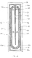
- Figure 1 is a composite sectional view of one embodiment of the planar magnetron sputtering device suitable for installation in an evacuable chamber.
- the apparatus comprises a magnet yoke 100 as the main structure of the cathode body.
- the magnet yoke is made of low carbon steel which provides magnetic shunt and physical strength.
- Target 105 which has a lower planar surface 106, is generally rectangular and is formed from the particular material to be sputtered. Common sputtering materials include metals such as titanium and zinc.
- the target is generally positioned to be parallel with the surface or surfaces upon which the sputtered deposit is to be made. Thus, a substrate to be coated would be supported a short distance from the lower target planar surface 106.
- the target is attached to the metal backing plate 110 that is preferably made of copper or any suitable material. Copper is preferred because it has high thermal conductivity and good mechanical properties.
- the upper surface of the target is bonded to the lower surface of the backing plate by soldering, brazing, using adhesives, or other bonding techniques.
- the lower surface of the backing plate preferably has substantially the same contour as the upper surface of the target so that the side surface of the target is substantially flush with the side surface of the backing plate. (For targets made of materials that are sufficiently strong and machinable, e.g. titanium or stainless steel, no backing plate is required.)
- the magnet means comprise a central elongated magnet 122 and outer magnets 121 and 123. It is understood that each magnet referred to, either 121, 122, or 123, preferably comprises a plurality of individual magnets. As will be described further below, the outer magnets 121 and 123 form a continuous, annular shaped magnet having an exterior side that is positioned adjacent to the edge of the backing plate. For a rectangularly shaped backing plate, the annular outer magnet will be adjacent to only a portion of the edge along the length of the backing plate.
- the polarity of the pole (facing the backing plate) of the inner magnet 122 is opposite to the polarity of poles (facing the backing plate) of the outer magnets 121 and 123.
- This arrangement creates a magnetic field which emerges from the target lower surface over one pole, curves over, and reenters the target over the opposite pole.
- the magnetic field is caused to travel in the characteristic closed loop that defines the "race-track" from which material is sputtered.
- the source area is larger than in a conventional planar magnetrons having a target with comparable surface area.
- the improved target utilisation is attributable in part to the fact that width of each of the magnets 121, 122, and 123 is relatively small relative to the width of the target lower surface and that the outer magnets are positioned at the edge of the backing plate. The result is that the closed loop magnetic field covers a larger percentage of the target surface.
- Figure 1 is a composite transverse sectional view of the planar magnetron and with the present invention the width of each magnet is preferably approximately 5.5% of the backing plate or target width.
- transverse section is meant a transverse section taken across a middle section of a rectangular planar magnetron that includes a cross section of the elongated inner magnet.
- the middle section of a rectangular planar magnetron includes those parts along the length of the magnetron where the upper backing plate surface (or the upper target surface, for embodiment that do not have a backing plate) supports both the inner and the outer magnets.
- the middle section corresponds to that part of the magnetron between the ends of the elongated inner magnet.
- each magnet is preferably less than approximately 6% of the target width and more preferably less than approximately 5.5%.
- the target has width W
- magnets 121, 122, and 123 have widths w 1 , w 2 , and W 3 , respectively, then w 1 , w 2 , and w 3 collectively should be equal to or less than about 0.18 W, and preferably equal to or less than about 0.165 W.
- magnets 121 and 123 comprise a single outer annual magnet, it is understood that reference to the width of the outer magnet(s) includes the widths of both magnets 121 and 123, collectively.
- the small width of each permanent magnet maximises the active target area from which target material can be sputtered.
- the low carbon steel yoke 100 has three projections or members. These are inner projection 102 and outer projections 101 and 103 which rest on magnets 122, 121, and 123, respectively.
- the backing plate 110 is secured to the yoke by a plurality of T-nuts 130 and bolts 131.
- the copper backing plate can be fabricated from a single, flat stock sheet with no brazing or soldering.
- the magnet yoke is mounted by a plurality of support ceramic rods 160 to side bars 141 and 142. The side bars are attached to a cover plate 170.
- the outer structures of the side bars can be releasably mounted to a vacuum chamber.
- the side bars 141 and 142 define a continuous frame-like outer structure around the perimeter of target cathode.
- the side bars have elongated members 143 and 144 which define secondary coolant channels 143A and 144A, respectively, through which coolant such as water is circulated. Coolant is delivered from inlets 145 and 146 and is removed through outlets (not shown).
- the side bars can function as anodes, but preferably, as shown, the anodes comprise of shadow bar 148 and member 143, that are welded together, on one side of the target and shadow bar 149 and member 144 on the other.
- Each shadow bar comprises a metallic plate that has a lower planar surface that is substantially coplanar with target surface 106. The shadow bars prevent condensate from accumulating in the dark space 165.
- Elongated members 143 and 144 are each electrically isolated from the remaining upper portions of side bar 141 and 142, respectively, by ceramic insulators.
- the magnet yoke also comprises extension structures 101a and 103a disposed along the side surfaces of the backing plate and target. As shown in Figure 1, the spacing between the extension structures and the side surface of the target is only about 0.031 inch (0.08 cm). These extensions shunt the magnetic field at the edges of the target. In addition, the side bars and extension structures define a dark space 165 around the cathode wherein no plasma forms. Excess magnetic field entering the dark space can cause arcing. As is apparent, extensions 101a and 103a of the magnet yoke obviate the need for having a separate cathode core structure.
- the permanent magnets can be made from any suitable material; NdFeB magnets are particularly suited. It was found that the presence of the extension structures 101a and 103a allows the NdFeB magnets to be smaller relative to conventional Alnico or ceramic magnets which in turn permits magnets 121 and 123 to be located closer to and more precisely at the edges along the length of the backing plate.
- the inventive device also comprises stainless steel inserts 150 and 153 which provide non-corrodible, non-magnetic sealing surfaces for gaskets 151 and 152. Insert 150 is welded to the magnet yoke as indicated by continuous vacuum tight weld joint 171.
- inner magnet 122 is an elongated structure that is centrally located (with respect to the outer annular magnet) and is lined by seal 139.
- Insert 180 is positioned juxtaposed to one end of the inner magnet. Coolant from inlet 137 enters channel 135 at a point near insert 180 and exits through outlet 138 that is located near the other side of the insert. Thus insert 180 directs the flow of the coolant and prevents cold coolant from mixing with hot coolant.
- Stainless steel insert 150 defines an annular structure positioned around insert 180 and the inner magnet; moreover, insert 150 and the inner magnet and insert 180 define primary coolant channels 135 and 136. Gasket 151 which is positioned in a groove defined by insert 150 prevents coolant from leaking into the vacuum chamber.
- bolt 131 which fit into holes in insert 150 secure the backing plate to the magnet yoke.
- the outer magnet pieces 121 and 123 form an annular structure having a inner contour that matches the outer contour of insert 150 so that the magnets fit close to the insert.
- the annular structure of the outer magnets also define an annular space wherein the elongated inner magnet is positioned to create the closed-loop magnetic field.
- Extensions 101a and 103a of the yoke form a rectangular frame-like structure that is positioned along the outer perimeter of the annular magnet.
- side bars 141 and 142 (shown schematically) is a rectangular frame-like structure that is positioned around the outer perimeter of the extension structures.
- a planar magnetron having the structures as shown in Figures 1 and 2 and having a titanium cathode target measuring 1 inch (2.54 cm) high, 7 inches (17.78 cm) wide, and 51 inches (129.54 cm) long was installed in an evacuable chamber. No backing plate is needed with the titanium target.
- a negative potential sufficient to cause sputtering to occur was supplied to the target from a D.C. power source.
- the anodes were either grounded or floating.
- Argon was used as the inert gas during sputtering; the argon pressure was kept at between 1 and 5 ⁇ m.
- the cathode assembly was used to sputter titanium metal film onto substrates.
- FIG. 3 is the graph of the percent thickness variation versus position along the width of the substrate for the titanium film sputtered onto a planar glass substrate.
- Curves 301 and 302 represent depositions wherein the anode was floated and curves 303 and 304 represent depositions wherein the anode was grounded.
- the graph depicts the deviation of film thickness from the average based on twelve measurements that were taken across the width of the coater.
- the substrate used was 44 inches (111.76 cm) in width and 12 glass slides were positioned approximately 4 inches apart along the width. After each substrate was coated with the titanium film, the thickness of the film on each slide was measured.
- Figure 4 is a graph illustrating the correlation between the temperature of the backing plate (measured at position 154 of Figure 1) and the power applied to the system. As is apparent, the temperature of the backing plate increases linearly with power. The temperature of the coolant water entering the system was approximately 23*C.
- Figure 5 is a graph illustrating the correlation between current and voltage for the system.
- Curve 501 is the IV curve when the anodes were grounded and curve 502 is the IV curve when the anodes were floated.
- the power used ranged from approximately 2 to 12 kW.
- Figure 6 shows the erosion pattern for the titanium target.
- the erosion groove for only one half of the target is illustrated although it was found that the erosion groove for the other half was practically identical.
- Erosion of the target was measured along a transverse section of the target at approximately the mid-point along the target's length.
- the erosion curve shows the sputtered profile of the titanium target when the above referenced system was operated at 20 kW in argon at 2 ⁇ m pressure after approximately 200 hours.
- the broadness of the erosion pattern demonstrates that the target material was sputtered relatively evenly from across the width of the target resulting in improved target utilisation.
- the target When a target is made of material, such as indium-tin oxide (ITO), which requires that the target be attached to a backing plate, the target is normally 0.5 inches (1.27 cm) thick and the backing plate is 0.375 inches (0.9525 cm) thick. Based on the erosion characteristics for the 1 inch (2.54 cm) thick titanium plate as shown in Figure 6, it is estimated that with the inventive planar magnetron the target utilisation is at least approximately 36% for targets that require backing plates.
- ITO indium-tin oxide
- the inventive device is that because the outer magnet poles are positioned at the extreme edge (or perimeter) of the backing plate, the outer boundary of the erosion region is substantially at the outer edge of the target. Moreover, the use of small magnets also allows for fine tuning of the magnet field strength along the length of the target for uniformity control. Furthermore, the relatively smaller NdFeB magnets create a relatively larger erosion region from which material is sputtered. In addition, measurements showed that the ratio of active target area to source area is approximately 0.65. (For conventional planar magnetrons that are greater than 1 meter long, this ratio is normally approximately 0.45.) The inventive planar magnetron can be operated in the A.C. mode; moreover, the apparatus can be employed in reactive sputtering wherein reactive gases are mixed with the inert gas to form film of metal compounds. For instance, the use of oxygen produces TiO 2 films when the target material is titanium.
- DDR dynamic deposition rate
- a backing plate (designated as structure 110 in Figure 1) was employed.
- no backing plate is used so that the structures designated as 105 and 110 in Figure 1 would instead be replaced by a single integral target. That is, instead of having two separate rectangular slabs (backing plate and target) bonded together, the second embodiment would have a single target structure without the backing plate.
- the dimensions of the target structure of the second embodiment preferably is equal to the combined dimensions of structures 105 and 110.
Landscapes
- Physics & Mathematics (AREA)
- Engineering & Computer Science (AREA)
- Plasma & Fusion (AREA)
- Chemical & Material Sciences (AREA)
- Analytical Chemistry (AREA)
- Physical Vapour Deposition (AREA)
Description
Claims (11)
- A planar magnetron device comprising:a target (105) having an upper target surface with an upper target perimeter, a planar lower target surface (106) of material to be sputtered, and a side surface;magnet means (121,122,123) positioned adjacent to and above the upper target surface for generating a closed-loop magnetic field over the lower target surface (106); anda magnet yoke (100) having an inner projection (102) and outer projections (101,103) that, together with said magnet yoke, define one or more primary coolant channels (135,136) that are in thermal communication with a portion of the upper target surface, in which the outer projections comprise extension means (101a,103a) that are positioned adjacent to the side surface of the target for shunting the magnetic field.
- A planar magnetron according to Claim 1 in which the magnet means comprises an inner magnet and outer magnets, in which the outer magnets are positioned adjacent to and along a portion of the upper target perimeter and in which the inner projection is attached to the inner magnet and the outer projections are attached to the outer magnets.
- A planar magnetron according to Claim 1 or Claim 2 further comprising side bar structures that are positioned adjacent to the side surface of the target, and in which the extension means and the side bar structures define a dark space therein between.
- A planar magnetron according to Claim 3 in which the side bar structures define one or more secondary coolant channels.
- A planar magnetron according to any one of Claims 2 to 4 in which the outer magnets comprise an annular structure defining an annular space and in which the inner magnet comprises an elongated inner magnet centrally located within the annular space.
- A planar magnetron according to any preceding claim in which the upper target surface is rectangularly shaped having a width equal to distance W and a length, in which the elongated inner magnet, which has a width equal to distance w1 along a transverse section of the target, is parallel with an edge of the target along the length of the target, in which the outer magnets have a collective width equal to distance w2 along a transverse section of the target, and in which w1 and w2 is equal to or less than about 18% of W.
- A planar magnetron according to any preceding claim further comprising a pair of elongated anode structures positioned on opposite sides of the target and in which each anode is evenly spaced from the target.
- A planar magnetron according to Claim 7 in which each of the elongated anode structures defines a planar anode surface that is coplanar with the planar lower target surface.
- A planar magnetron according to any preceding claim in which the magnet means comprises NdFeB magnets.
- A planar magnetron according to any preceding claim in which the target comprises a backing plate having a lower backing plate surface attached to the material to be sputtered and an upper backing plate surface that defines the upper target surface.
- A planar magnetron according to Claim 10 in which the backing plate is made of copper.
Applications Claiming Priority (2)
| Application Number | Priority Date | Filing Date | Title |
|---|---|---|---|
| US08/090,916 US5407551A (en) | 1993-07-13 | 1993-07-13 | Planar magnetron sputtering apparatus |
| US90916 | 1993-07-13 |
Publications (2)
| Publication Number | Publication Date |
|---|---|
| EP0634500A1 EP0634500A1 (en) | 1995-01-18 |
| EP0634500B1 true EP0634500B1 (en) | 1998-05-20 |
Family
ID=22224947
Family Applications (1)
| Application Number | Title | Priority Date | Filing Date |
|---|---|---|---|
| EP94304676A Expired - Lifetime EP0634500B1 (en) | 1993-07-13 | 1994-06-27 | Planar magnetron sputtering apparatus |
Country Status (6)
| Country | Link |
|---|---|
| US (1) | US5407551A (en) |
| EP (1) | EP0634500B1 (en) |
| JP (1) | JP3547485B2 (en) |
| KR (1) | KR960015666A (en) |
| CA (1) | CA2125532A1 (en) |
| DE (1) | DE69410358T2 (en) |
Families Citing this family (39)
| Publication number | Priority date | Publication date | Assignee | Title |
|---|---|---|---|---|
| US5736019A (en) | 1996-03-07 | 1998-04-07 | Bernick; Mark A. | Sputtering cathode |
| WO1999025892A1 (en) | 1997-11-19 | 1999-05-27 | Tosoh Smd, Inc. | METHOD FOR MAKING Ni-Si MAGNETRON SPUTTERING TARGETS AND TARGETS MADE THEREBY |
| AU9410498A (en) * | 1997-11-26 | 1999-06-17 | Vapor Technologies, Inc. | Apparatus for sputtering or arc evaporation |
| RU2160323C2 (en) * | 1998-02-19 | 2000-12-10 | Иркутский государственный педагогический университет | Plant for ion-plasma spraying |
| US6359388B1 (en) | 2000-08-28 | 2002-03-19 | Guardian Industries Corp. | Cold cathode ion beam deposition apparatus with segregated gas flow |
| US6495000B1 (en) * | 2001-07-16 | 2002-12-17 | Sharp Laboratories Of America, Inc. | System and method for DC sputtering oxide films with a finned anode |
| US6988463B2 (en) * | 2002-10-18 | 2006-01-24 | Guardian Industries Corp. | Ion beam source with gas introduced directly into deposition/vacuum chamber |
| US6812648B2 (en) | 2002-10-21 | 2004-11-02 | Guardian Industries Corp. | Method of cleaning ion source, and corresponding apparatus/system |
| KR20050118313A (en) * | 2003-05-02 | 2005-12-16 | 토소우 에스엠디, 인크 | Methods for making low silicon content ni-si sputtering targets and targets made thereby |
| US7297247B2 (en) * | 2003-05-06 | 2007-11-20 | Applied Materials, Inc. | Electroformed sputtering target |
| US7910218B2 (en) | 2003-10-22 | 2011-03-22 | Applied Materials, Inc. | Cleaning and refurbishing chamber components having metal coatings |
| US7670436B2 (en) | 2004-11-03 | 2010-03-02 | Applied Materials, Inc. | Support ring assembly |
| US7087145B1 (en) * | 2005-03-10 | 2006-08-08 | Robert Choquette | Sputtering cathode assembly |
| US8470141B1 (en) * | 2005-04-29 | 2013-06-25 | Angstrom Sciences, Inc. | High power cathode |
| US8617672B2 (en) | 2005-07-13 | 2013-12-31 | Applied Materials, Inc. | Localized surface annealing of components for substrate processing chambers |
| US7762114B2 (en) * | 2005-09-09 | 2010-07-27 | Applied Materials, Inc. | Flow-formed chamber component having a textured surface |
| US9127362B2 (en) | 2005-10-31 | 2015-09-08 | Applied Materials, Inc. | Process kit and target for substrate processing chamber |
| US20070125646A1 (en) * | 2005-11-25 | 2007-06-07 | Applied Materials, Inc. | Sputtering target for titanium sputtering chamber |
| EP1826811A1 (en) * | 2006-02-22 | 2007-08-29 | Applied Materials GmbH & Co. KG | Cooled target sputtering |
| EP1835525A1 (en) * | 2006-03-16 | 2007-09-19 | Sulzer Metco AG (Switzerland) | Target gripping device |
| CA2577757A1 (en) * | 2006-03-16 | 2007-09-16 | Sulzer Metco Ag | Target holding apparatus |
| US20070283884A1 (en) * | 2006-05-30 | 2007-12-13 | Applied Materials, Inc. | Ring assembly for substrate processing chamber |
| US8961756B2 (en) * | 2006-08-04 | 2015-02-24 | Applied Materials, Inc. | Ganged scanning of multiple magnetrons, especially two level folded magnetrons |
| KR100910673B1 (en) * | 2006-08-04 | 2009-08-04 | 어플라이드 머티어리얼스, 인코포레이티드 | Ganged scanning of multiple magnetrons, especially two level folded magnetrons |
| US7981262B2 (en) | 2007-01-29 | 2011-07-19 | Applied Materials, Inc. | Process kit for substrate processing chamber |
| US7942969B2 (en) | 2007-05-30 | 2011-05-17 | Applied Materials, Inc. | Substrate cleaning chamber and components |
| US8968536B2 (en) * | 2007-06-18 | 2015-03-03 | Applied Materials, Inc. | Sputtering target having increased life and sputtering uniformity |
| US7901552B2 (en) * | 2007-10-05 | 2011-03-08 | Applied Materials, Inc. | Sputtering target with grooves and intersecting channels |
| US8575565B2 (en) | 2011-10-10 | 2013-11-05 | Guardian Industries Corp. | Ion source apparatus and methods of using the same |
| US9347129B2 (en) | 2011-12-09 | 2016-05-24 | Seagate Technology Llc | Interchangeable magnet pack |
| US10573500B2 (en) | 2011-12-09 | 2020-02-25 | Seagate Technology Llc | Interchangeable magnet pack |
| US9476118B2 (en) | 2012-12-10 | 2016-10-25 | Angstrom Sciences, Inc. | Adjustable shunt assembly for a sputtering magnetron and a method for adjusting such a shunt |
| DE202014006417U1 (en) | 2014-08-11 | 2014-08-20 | Grenzebach Maschinenbau Gmbh | Device for saving energy and at the same time increasing the throughput speed in vacuum coating systems |
| DE102014011877B4 (en) | 2014-08-11 | 2021-08-05 | Grenzebach Maschinenbau Gmbh | Method and device for saving energy and at the same time increasing the throughput speed in vacuum coating systems |
| WO2016069490A1 (en) | 2014-10-29 | 2016-05-06 | General Plasma, Inc. | Magnetic anode for sputter magnetron cathode |
| RU176970U1 (en) * | 2017-04-14 | 2018-02-05 | федеральное государственное бюджетное образовательное учреждение высшего образования "Ижевский государственный технический университет имени М.Т. Калашникова" | RING PLANAR MAGNETRON |
| TWI641712B (en) * | 2017-12-04 | 2018-11-21 | 國家中山科學研究院 | Heating stage device applied to sputtering target gun |
| CN109161819B (en) * | 2018-09-20 | 2020-07-07 | 京磁材料科技股份有限公司 | Preparation method of sintered neodymium-iron-boron magnet with low carbon content |
| CN120758845B (en) * | 2025-07-08 | 2026-03-24 | 上海源创同章表面涂层科技有限公司 | A strip planar magnetron cathode with high target utilization |
Family Cites Families (14)
| Publication number | Priority date | Publication date | Assignee | Title |
|---|---|---|---|---|
| US4166018A (en) * | 1974-01-31 | 1979-08-28 | Airco, Inc. | Sputtering process and apparatus |
| US3956093A (en) * | 1974-12-16 | 1976-05-11 | Airco, Inc. | Planar magnetron sputtering method and apparatus |
| US4198283A (en) * | 1978-11-06 | 1980-04-15 | Materials Research Corporation | Magnetron sputtering target and cathode assembly |
| DE3047113A1 (en) * | 1980-12-13 | 1982-07-29 | Leybold-Heraeus GmbH, 5000 Köln | Cathode arrangement and control method for cathode sputtering systems with a magnet system for increasing the sputtering rate |
| US4515675A (en) * | 1983-07-06 | 1985-05-07 | Leybold-Heraeus Gmbh | Magnetron cathode for cathodic evaportion apparatus |
| DE3480245D1 (en) * | 1983-12-05 | 1989-11-23 | Leybold Ag | Magnetron-cathodes for the sputtering of ferromagnetic targets |
| US4657654A (en) * | 1984-05-17 | 1987-04-14 | Varian Associates, Inc. | Targets for magnetron sputter device having separate confining magnetic fields to separate targets subject to separate discharges |
| US4834860A (en) * | 1987-07-01 | 1989-05-30 | The Boc Group, Inc. | Magnetron sputtering targets |
| US4892633A (en) * | 1988-11-14 | 1990-01-09 | Vac-Tec Systems, Inc. | Magnetron sputtering cathode |
| DE3844064A1 (en) * | 1988-12-28 | 1990-07-05 | Leybold Ag | MAGNETRON PRINCIPLE CATALOG SPRAYING DEVICE WITH A HOLLOW CATODE AND A CYLINDRICAL TARGET |
| DE3908252C2 (en) * | 1989-03-14 | 1996-06-20 | Leybold Ag | Atomizing cathode based on the magnetron principle |
| DE3929695C2 (en) * | 1989-09-07 | 1996-12-19 | Leybold Ag | Device for coating a substrate |
| US5180478A (en) * | 1990-12-19 | 1993-01-19 | Intevac, Inc. | Sputter coating source |
| DE4127260C1 (en) * | 1991-08-17 | 1992-04-16 | Forschungsgesellschaft Fuer Elektronenstrahl- Und Plasmatechnik Mbh, O-8051 Dresden, De | Magnetron sputter source |
-
1993
- 1993-07-13 US US08/090,916 patent/US5407551A/en not_active Expired - Lifetime
-
1994
- 1994-06-09 CA CA002125532A patent/CA2125532A1/en not_active Abandoned
- 1994-06-27 EP EP94304676A patent/EP0634500B1/en not_active Expired - Lifetime
- 1994-06-27 DE DE69410358T patent/DE69410358T2/en not_active Expired - Fee Related
- 1994-07-12 JP JP15989294A patent/JP3547485B2/en not_active Expired - Fee Related
- 1994-07-12 KR KR1019940016757A patent/KR960015666A/en not_active Ceased
Also Published As
| Publication number | Publication date |
|---|---|
| EP0634500A1 (en) | 1995-01-18 |
| US5407551A (en) | 1995-04-18 |
| KR960015666A (en) | 1996-05-22 |
| DE69410358D1 (en) | 1998-06-25 |
| JP3547485B2 (en) | 2004-07-28 |
| CA2125532A1 (en) | 1995-01-14 |
| JPH0754144A (en) | 1995-02-28 |
| DE69410358T2 (en) | 1998-12-03 |
Similar Documents
| Publication | Publication Date | Title |
|---|---|---|
| EP0634500B1 (en) | Planar magnetron sputtering apparatus | |
| US4198283A (en) | Magnetron sputtering target and cathode assembly | |
| US4200510A (en) | Assembly and method to extend useful life of sputtering targets | |
| CA1206914A (en) | Sputtering cathode apparatus | |
| US5876576A (en) | Apparatus for sputtering magnetic target materials | |
| EP0051635B1 (en) | Sputter target and glow discharge coating apparatus | |
| EP1390964B1 (en) | Dipole ion source | |
| CA2254677C (en) | Apparatus for sputtering or arc evaporation | |
| JPH05209266A (en) | Magnetron-sputter-gun-target-assembly having distributed magnetic field | |
| US6146509A (en) | Inverted field circular magnetron sputtering device | |
| EP0737999B1 (en) | A magnetron sputtering system | |
| CN1066851C (en) | Magnetic field cathode | |
| JPH0359138B2 (en) | ||
| US20030164288A1 (en) | Magnetron sputtering target for magnetic materials | |
| EP0451642B1 (en) | Sputtering system | |
| US7023128B2 (en) | Dipole ion source | |
| US5441614A (en) | Method and apparatus for planar magnetron sputtering | |
| US20120000424A1 (en) | Cooled dark space shield for multi-cathode design | |
| Spencer et al. | The design and performance of planar magnetron sputtering cathodes | |
| RU2242821C2 (en) | Magnetron spraying system | |
| GB2110719A (en) | Sputtering apparatus | |
| EP0197770A2 (en) | Planar penning magnetron sputtering device | |
| US20240191341A1 (en) | Stable ground anode aperture for thin film processing | |
| WO2024123879A1 (en) | Stable ground anode for thin film processing | |
| RU2074904C1 (en) | Cathode joint for ionic-plasma application of thin films in vacuum |
Legal Events
| Date | Code | Title | Description |
|---|---|---|---|
| PUAI | Public reference made under article 153(3) epc to a published international application that has entered the european phase |
Free format text: ORIGINAL CODE: 0009012 |
|
| AK | Designated contracting states |
Kind code of ref document: A1 Designated state(s): BE DE ES FR GB LU NL |
|
| 17P | Request for examination filed |
Effective date: 19950704 |
|
| GRAG | Despatch of communication of intention to grant |
Free format text: ORIGINAL CODE: EPIDOS AGRA |
|
| 17Q | First examination report despatched |
Effective date: 19970811 |
|
| GRAG | Despatch of communication of intention to grant |
Free format text: ORIGINAL CODE: EPIDOS AGRA |
|
| GRAH | Despatch of communication of intention to grant a patent |
Free format text: ORIGINAL CODE: EPIDOS IGRA |
|
| GRAH | Despatch of communication of intention to grant a patent |
Free format text: ORIGINAL CODE: EPIDOS IGRA |
|
| GRAA | (expected) grant |
Free format text: ORIGINAL CODE: 0009210 |
|
| AK | Designated contracting states |
Kind code of ref document: B1 Designated state(s): BE DE ES FR GB LU NL |
|
| PG25 | Lapsed in a contracting state [announced via postgrant information from national office to epo] |
Ref country code: FR Free format text: LAPSE BECAUSE OF FAILURE TO SUBMIT A TRANSLATION OF THE DESCRIPTION OR TO PAY THE FEE WITHIN THE PRESCRIBED TIME-LIMIT Effective date: 19980520 |
|
| REF | Corresponds to: |
Ref document number: 69410358 Country of ref document: DE Date of ref document: 19980625 |
|
| PGFP | Annual fee paid to national office [announced via postgrant information from national office to epo] |
Ref country code: FR Payment date: 19980720 Year of fee payment: 5 |
|
| PGFP | Annual fee paid to national office [announced via postgrant information from national office to epo] |
Ref country code: ES Payment date: 19980730 Year of fee payment: 5 |
|
| PGFP | Annual fee paid to national office [announced via postgrant information from national office to epo] |
Ref country code: LU Payment date: 19980902 Year of fee payment: 5 |
|
| EN | Fr: translation not filed | ||
| PG25 | Lapsed in a contracting state [announced via postgrant information from national office to epo] |
Ref country code: ES Free format text: LAPSE BECAUSE OF FAILURE TO SUBMIT A TRANSLATION OF THE DESCRIPTION OR TO PAY THE FEE WITHIN THE PRESCRIBED TIME-LIMIT Effective date: 19981118 |
|
| PLBE | No opposition filed within time limit |
Free format text: ORIGINAL CODE: 0009261 |
|
| STAA | Information on the status of an ep patent application or granted ep patent |
Free format text: STATUS: NO OPPOSITION FILED WITHIN TIME LIMIT |
|
| 26N | No opposition filed | ||
| PG25 | Lapsed in a contracting state [announced via postgrant information from national office to epo] |
Ref country code: LU Free format text: LAPSE BECAUSE OF NON-PAYMENT OF DUE FEES Effective date: 19990627 |
|
| REG | Reference to a national code |
Ref country code: GB Ref legal event code: IF02 |
|
| PGFP | Annual fee paid to national office [announced via postgrant information from national office to epo] |
Ref country code: NL Payment date: 20020610 Year of fee payment: 9 |
|
| PGFP | Annual fee paid to national office [announced via postgrant information from national office to epo] |
Ref country code: GB Payment date: 20020619 Year of fee payment: 9 |
|
| PG25 | Lapsed in a contracting state [announced via postgrant information from national office to epo] |
Ref country code: GB Free format text: LAPSE BECAUSE OF NON-PAYMENT OF DUE FEES Effective date: 20030627 |
|
| PGFP | Annual fee paid to national office [announced via postgrant information from national office to epo] |
Ref country code: BE Payment date: 20030902 Year of fee payment: 10 |
|
| PG25 | Lapsed in a contracting state [announced via postgrant information from national office to epo] |
Ref country code: NL Free format text: LAPSE BECAUSE OF NON-PAYMENT OF DUE FEES Effective date: 20040101 |
|
| GBPC | Gb: european patent ceased through non-payment of renewal fee |
Effective date: 20030627 |
|
| NLV4 | Nl: lapsed or anulled due to non-payment of the annual fee |
Effective date: 20040101 |
|
| PG25 | Lapsed in a contracting state [announced via postgrant information from national office to epo] |
Ref country code: BE Free format text: LAPSE BECAUSE OF NON-PAYMENT OF DUE FEES Effective date: 20040630 |
|
| PGFP | Annual fee paid to national office [announced via postgrant information from national office to epo] |
Ref country code: DE Payment date: 20040701 Year of fee payment: 11 |
|
| BERE | Be: lapsed |
Owner name: THE *BOC GROUP INC. Effective date: 20040630 |
|
| PG25 | Lapsed in a contracting state [announced via postgrant information from national office to epo] |
Ref country code: DE Free format text: LAPSE BECAUSE OF NON-PAYMENT OF DUE FEES Effective date: 20060103 |