EP0637871A1 - Surface acoustic wave device mounted module - Google Patents
Surface acoustic wave device mounted module Download PDFInfo
- Publication number
- EP0637871A1 EP0637871A1 EP94112070A EP94112070A EP0637871A1 EP 0637871 A1 EP0637871 A1 EP 0637871A1 EP 94112070 A EP94112070 A EP 94112070A EP 94112070 A EP94112070 A EP 94112070A EP 0637871 A1 EP0637871 A1 EP 0637871A1
- Authority
- EP
- European Patent Office
- Prior art keywords
- acoustic wave
- surface acoustic
- wave element
- device mounted
- multilayer substrate
- Prior art date
- Legal status (The legal status is an assumption and is not a legal conclusion. Google has not performed a legal analysis and makes no representation as to the accuracy of the status listed.)
- Granted
Links
Images


Classifications
-
- H—ELECTRICITY
- H03—ELECTRONIC CIRCUITRY
- H03H—IMPEDANCE NETWORKS, e.g. RESONANT CIRCUITS; RESONATORS
- H03H9/00—Networks comprising electromechanical or electro-acoustic elements; Electromechanical resonators
- H03H9/02—Details
- H03H9/05—Holders or supports
- H03H9/10—Mounting in enclosures
- H03H9/1064—Mounting in enclosures for surface acoustic wave [SAW] devices
- H03H9/1071—Mounting in enclosures for surface acoustic wave [SAW] devices the enclosure being defined by a frame built on a substrate and a cap, the frame having no mechanical contact with the SAW device
-
- H—ELECTRICITY
- H03—ELECTRONIC CIRCUITRY
- H03H—IMPEDANCE NETWORKS, e.g. RESONANT CIRCUITS; RESONATORS
- H03H9/00—Networks comprising electromechanical or electro-acoustic elements; Electromechanical resonators
- H03H9/02—Details
- H03H9/05—Holders or supports
- H03H9/0538—Constructional combinations of supports or holders with electromechanical or other electronic elements
- H03H9/0542—Constructional combinations of supports or holders with electromechanical or other electronic elements consisting of a lateral arrangement
-
- H—ELECTRICITY
- H03—ELECTRONIC CIRCUITRY
- H03H—IMPEDANCE NETWORKS, e.g. RESONANT CIRCUITS; RESONATORS
- H03H9/00—Networks comprising electromechanical or electro-acoustic elements; Electromechanical resonators
- H03H9/02—Details
- H03H9/05—Holders or supports
- H03H9/0538—Constructional combinations of supports or holders with electromechanical or other electronic elements
- H03H9/0547—Constructional combinations of supports or holders with electromechanical or other electronic elements consisting of a vertical arrangement
- H03H9/0557—Constructional combinations of supports or holders with electromechanical or other electronic elements consisting of a vertical arrangement the other elements being buried in the substrate
-
- H—ELECTRICITY
- H03—ELECTRONIC CIRCUITRY
- H03H—IMPEDANCE NETWORKS, e.g. RESONANT CIRCUITS; RESONATORS
- H03H9/00—Networks comprising electromechanical or electro-acoustic elements; Electromechanical resonators
- H03H9/02—Details
- H03H9/05—Holders or supports
- H03H9/058—Holders or supports for surface acoustic wave devices
- H03H9/059—Holders or supports for surface acoustic wave devices consisting of mounting pads or bumps
-
- H—ELECTRICITY
- H03—ELECTRONIC CIRCUITRY
- H03H—IMPEDANCE NETWORKS, e.g. RESONANT CIRCUITS; RESONATORS
- H03H9/00—Networks comprising electromechanical or electro-acoustic elements; Electromechanical resonators
- H03H9/02—Details
- H03H9/05—Holders or supports
- H03H9/10—Mounting in enclosures
- H03H9/1064—Mounting in enclosures for surface acoustic wave [SAW] devices
- H03H9/1085—Mounting in enclosures for surface acoustic wave [SAW] devices the enclosure being defined by a non-uniform sealing mass covering the non-active sides of the SAW device
-
- H—ELECTRICITY
- H10—SEMICONDUCTOR DEVICES; ELECTRIC SOLID-STATE DEVICES NOT OTHERWISE PROVIDED FOR
- H10W—GENERIC PACKAGES, INTERCONNECTIONS, CONNECTORS OR OTHER CONSTRUCTIONAL DETAILS OF DEVICES COVERED BY CLASS H10
- H10W70/00—Package substrates; Interposers; Redistribution layers [RDL]
- H10W70/60—Insulating or insulated package substrates; Interposers; Redistribution layers
- H10W70/62—Insulating or insulated package substrates; Interposers; Redistribution layers characterised by their interconnections
- H10W70/63—Vias, e.g. via plugs
-
- H—ELECTRICITY
- H10—SEMICONDUCTOR DEVICES; ELECTRIC SOLID-STATE DEVICES NOT OTHERWISE PROVIDED FOR
- H10W—GENERIC PACKAGES, INTERCONNECTIONS, CONNECTORS OR OTHER CONSTRUCTIONAL DETAILS OF DEVICES COVERED BY CLASS H10
- H10W72/00—Interconnections or connectors in packages
- H10W72/851—Dispositions of multiple connectors or interconnections
- H10W72/853—On the same surface
- H10W72/856—Bump connectors and die-attach connectors
-
- H—ELECTRICITY
- H10—SEMICONDUCTOR DEVICES; ELECTRIC SOLID-STATE DEVICES NOT OTHERWISE PROVIDED FOR
- H10W—GENERIC PACKAGES, INTERCONNECTIONS, CONNECTORS OR OTHER CONSTRUCTIONAL DETAILS OF DEVICES COVERED BY CLASS H10
- H10W72/00—Interconnections or connectors in packages
- H10W72/851—Dispositions of multiple connectors or interconnections
- H10W72/874—On different surfaces
- H10W72/877—Bump connectors and die-attach connectors
-
- H—ELECTRICITY
- H10—SEMICONDUCTOR DEVICES; ELECTRIC SOLID-STATE DEVICES NOT OTHERWISE PROVIDED FOR
- H10W—GENERIC PACKAGES, INTERCONNECTIONS, CONNECTORS OR OTHER CONSTRUCTIONAL DETAILS OF DEVICES COVERED BY CLASS H10
- H10W74/00—Encapsulations, e.g. protective coatings
- H10W74/10—Encapsulations, e.g. protective coatings characterised by their shape or disposition
- H10W74/15—Encapsulations, e.g. protective coatings characterised by their shape or disposition on active surfaces of flip-chip devices, e.g. underfills
-
- H—ELECTRICITY
- H10—SEMICONDUCTOR DEVICES; ELECTRIC SOLID-STATE DEVICES NOT OTHERWISE PROVIDED FOR
- H10W—GENERIC PACKAGES, INTERCONNECTIONS, CONNECTORS OR OTHER CONSTRUCTIONAL DETAILS OF DEVICES COVERED BY CLASS H10
- H10W90/00—Package configurations
- H10W90/701—Package configurations characterised by the relative positions of pads or connectors relative to package parts
- H10W90/721—Package configurations characterised by the relative positions of pads or connectors relative to package parts of bump connectors
- H10W90/724—Package configurations characterised by the relative positions of pads or connectors relative to package parts of bump connectors between a chip and a stacked insulating package substrate, interposer or RDL
-
- H—ELECTRICITY
- H10—SEMICONDUCTOR DEVICES; ELECTRIC SOLID-STATE DEVICES NOT OTHERWISE PROVIDED FOR
- H10W—GENERIC PACKAGES, INTERCONNECTIONS, CONNECTORS OR OTHER CONSTRUCTIONAL DETAILS OF DEVICES COVERED BY CLASS H10
- H10W90/00—Package configurations
- H10W90/701—Package configurations characterised by the relative positions of pads or connectors relative to package parts
- H10W90/731—Package configurations characterised by the relative positions of pads or connectors relative to package parts of die-attach connectors
- H10W90/734—Package configurations characterised by the relative positions of pads or connectors relative to package parts of die-attach connectors between a chip and a stacked insulating package substrate, interposer or RDL
Definitions
- the invention relates to a surface acoustic wave device mounted module for mobile communication equipment.
- a conventional surface acoustic wave (SAW) device mounted module for example, is described in IEEE Transactions on Vehicular Technology, vol. 38, No. 1 (1989), pp.2-8.
- This conventional SAW device mounted module has a surface acoustic wave element mounted on a can-like package.
- An aluminum wire provides continuity across the input-output terminals of the package and the surface acoustic wave element.
- a package which can be mounted on plates such as a ceramic package has recently been requested, particularly for mobile communication equipment.
- a bonding wire is required to establish continuity with surface acoustic wave element. Therefore, the miniaturization of a SAW device mounted module is limited when one of these packages is used for the SAW device mounted module, since the height of the bonding wire is limited and a land for the bonding wire is required on the package.
- a face down bonding (or flip chip bonding) is used as a method of miniaturizing a SAW device mounted module.
- the surface acoustic wave element faces a circuit substrate and conductive bumps are used to establish continuity across the element and the substrate. In other words, a bonding wire is not required in this method.
- a surface acoustic wave element applied for mobile communication equipment uses a piezoelectric substrate with high pyroelectricity, so that when a frequency band (pass band frequency for a surface acoustic wave element used as a band pass filter) is high, the line width of an inter-digital transducer (IDT) used for the element ranges from 0.5 ⁇ m to 1 ⁇ m. Therefore, when the temperature changes by processes of forming conductive bumps, the IDT is likely to be broken by the pyroelectricity of the substrate.
- a space around the surface acoustic wave element is required for smooth propagation of surface acoustic waves along the functional surface of the element.
- a surface acoustic wave element is combined with a matching circuit or integrated with other parts.
- the combination of the element with the matching circuit is particularly required when the element is used as an IF (intermediate frequency) filter for mobile communication equipment. If the IF filter is applied as a surface acoustic wave element, input-output impedances generally become high so that an impedance matching circuit is required to connect the element with an outside circuit.
- An example of an integrated circuit including a surface acoustic wave element (IF section) is mentioned in Proceedings on Ultrasonics Symposium (1986), pp. 283-288. In this example, packaged devices are integrated with each other into one body so that this method is not effective in miniaturizing mobile communication equipment.
- a conventional SAW device mounted module disclosed in Published Unexamined Japanese Patent Application No. Hei 5-291864 is manufactured by the steps of: forming gold or aluminum bumps on electrode pads of a surface acoustic wave element; transfer-coating a conductive resin on top of the bumps; placing the bumps on the surface of a ceramic substrate formed with a wiring pattern; heating and curing the conductive resin to bond the element to the ceramic substrate; and adding an insulating resin around the element to increase the adhesion between the element and the substrate.
- this conventional SAW device mounted module a space is provided around the IDT of the SAW element, and the viscosity of insulating resin is arranged to prevent adhesion of the resin to the IDT.
- a metal lid is attached to the substrate by an insulating resin and the SAW element is kept in an airtight condition.
- This conventional SAW device mounted module includes a monolayer ceramic substrate, and only a two-dimensional wiring is used with this SAW device mounted module. Therefore, the size of the SAW device mounted module is large when an impedance matching circuit is formed on the ceramic substrate or when a module is formed by integrating the surface acoustic wave element with other parts. Since a wiring pattern is formed on the surface of the ceramic substrate, a metal lid cannot be sealed by a conductive material, so the electromagnetic shield of this conventional SAW device mounted module becomes insignificant.
- This invention provides a surface acoustic wave device mounted module which is miniature, lightweight, and highly reliable.
- the SAW device mounted module also has excellent frequency characteristics.
- the surface acoustic wave device mounted module of the invention comprises a multilayer substrate which includes at least one layer of a shield pattern, input-output electrodes, grounding electrodes and via holes used for connecting the electrodes; and a surface acoustic wave element placing an inter-digital transducer to face the multilayer substrate and having metallic bumps, which are transfer-coated with a conductive resin, on electrode pads and an insulating resin around the surface acoustic wave element.
- the electrode pads are input-output terminals and grounding terminals formed on the surface acoustic wave element.
- An electrode pattern is formed on the surface of the multilayer substrate to surround the surface acoustic wave element.
- a metallic lid is attached to the electrode pattern by a solder or a conductive resin so that the surface acoustic wave element is sealed in an airtight condition by the metallic lid.
- the electrode pattern is connected to the grounding electrodes by the via holes.
- the surface acoustic wave element is a piezoelectric substrate and that the piezoelectric substrate is at least one material selected from the group consisting of lithium tantalate, lithium niobate, lithium borate, and quartz.
- an electrode pattern is formed on the multilayer substrate to face the inter-digital transducer of the surface acoustic wave element and that a continuity is established between the electrode pattern and the grounding electrodes or the shield pattern by the via holes.
- a conductive film is formed on the top surface of the surface acoustic wave element and that a continuity is established between the metallic lid and the top surface by the conductive film.
- a continuity is established between the top surface of the surface acoustic wave element and the metallic lid by a conductive resin.
- the bumps are made of at least one metal selected from the group consisting of gold and aluminum.
- the surface acoustic wave element is mounted on the flat surface of the multilayer substrate.
- the surface acoustic wave element is mounted on the depression in the multilayer substrate.
- a circuit element is applied to the multilayer substrate to match with the input-output impedances of an outside circuit.
- the invention also provides a surface acoustic wave device mounted module comprising a multilayer substrate which includes at least one layer of shield pattern, input-output electrodes, grounding electrodes, and via holes used for connecting the electrodes; a surface acoustic wave element placing an inter-digital transducer to face the multilayer substrate and having metallic bumps, which are transfer-coated with a conductive resin, on electrode pads and an insulating resin partially or entirely surrounding the surface acoustic wave element; and other active or passive components.
- the electrode pads are input-output terminals and grounding terminals formed on the surface acoustic wave element.
- the surface acoustic wave element and the other active or passive components are integrated in one body on the multilayer substrate.
- An electrode pattern is formed on the multi layer substrate to surround the surface acoustic wave element.
- a metallic lid is attached to the electrode pattern by a solder or a conductive resin to seal the surface acoustic wave element in an airtight condition.
- the electrode pattern is connected to the grounding electrodes by the via holes.
- the surface acoustic wave element is mounted on the depression in the multilayer substrate.
- the electrode pattern is formed on the multilayer substrate to surround the surface acoustic wave element and the active or passive components in one body.
- the bumps are made of at least one metal selected from the group consisting of gold and aluminum.
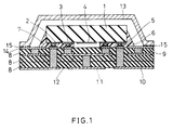
- Fig. 1 is a cross sectional view of a surface acoustic wave device mounted module of a first embodiment of the invention.
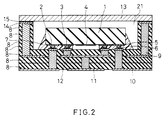
- Fig. 2 is a cross sectional view of a surface acoustic wave device mounted module of a second embodiment of the invention.
- Fig. 3 is a cross sectional view of a surface acoustic wave device mounted module of a third embodiment of the invention.
- Fig. 4 is a cross sectional view of a surface acoustic wave device mounted module of a fourth embodiment of the invention.
- Fig. 5 is a cross sectional view of a surface acoustic wave device mounted module of a fifth embodiment of the invention.
- Fig. 6 is a cross sectional view of a surface acoustic wave device mounted module of a sixth embodiment of the invention.
- Fig. 7 is a cross sectional view of a surface acoustic wave device mounted module of a seventh embodiment of the invention.
- FIG. 1 shows a cross-sectional view of a surface acoustic wave device mounted module of a first embodiment.
- a surface acoustic wave element 1 is a piezoelectric substrate made of at least one material selected from the group consisting of lithium niobate, lithium tantalate, lithium borate, and quartz.
- An input-output terminal 2, a grounding terminal 3, and an inter-digital transducer (IDT) 4 are formed on surface acoustic wave element 1 by a conventional photolithography.
- These elements are made of aluminum alloy or gold alloy.
- 5 is a gold or aluminum bump
- 6 is a conductive resin
- 7 is an insulating resin
- 8 is a multilayer substrate.
- the insulating resin 7 is used to increase the adhesion of the SAW element 1 to the substrate.
- a via hole 9, an input-output electrode 10, a grounding electrode 11, and a shield pattern 12 are applied to multilayer substrate 8 and form a conductor substantially made of silver or copper.
- a metallic lid 13 is attached to a grounding electrode pattern 14 by a conductive adhesive layer 15 comprising a conductive resin or a solder.
- Grounding electrode pattern 14 is formed on the surface of multilayer substrate 8, which faces surface acoustic wave element 1, and surrounds the element.
- the surface acoustic wave device mounted module can shield electromagnetic energy more efficiently than a conventional surface acoustic wave device mounted module and has excellent electrical characteristics.
- the surface acoustic wave device mounted module was manufactured by the following steps: forming metallic IDT 4 mainly made of aluminum, input-output terminals 2 and grounding terminals 3 on one surface of a 360Y-X lithium tantalate piezoelectric substrate (surface acoustic wave element 1) by a conventional photolithography, thus forming a multielectrode surface acoustic wave filter, which can be used as an interstage filter for mobile communication equipment; attaching metal wires about 25 ⁇ m in diameter on electrode pads (input-output terminals 2 and grounding terminals 3) by a conventional ball bonding machine to form conductive bumps 5 about 80 ⁇ m in bottom surface diameter and about 50 ⁇ m in height; facing the bumps towards a horizontal base and adding about 5g weight on each conductive bump 5 to limit the difference in height of the bumps to within 45 ⁇ 1 ⁇ m; dipping
- An alumina-glass ceramic was used as a dielectric for multilayer substrate 8.
- a copper electrode which was prepared by baking a copper oxide paste in a reducing atmosphere, was used for via hole 9 and shield pattern 12 as an inside electrode. It is, however, preferable to use an electrode paste containing glass for via hole 9 to provide an improved airtight condition in the via hole.
- a copper electrode plated with nickel/gold was used for the electrodes, which were formed on multilayer substrate 8 and were connected to input-output electrodes 10 by via holes, and the electrodes, which were formed on the substrate and were connected to grounding electrodes 11 by via holes, as an outside electrode.
- grounding electrode pattern 14 was connected to shield patterns 12 by via holes 9, and metallic lid 13 was adhered to the grounding electrode pattern. Therefore, an electromagnetic shield was provided at the surface acoustic wave device mounted module.
- the surface acoustic wave device mounted module had proper frequency characteristics. Also, by applying a grounding electrode pattern between the input and output electrodes on the multilayer substrate, the electromagnetic shield can be improved. Compared with a conventional surface acoustic wave device mounted module, the surface acoustic wave device mounted module of the example had an improvement in stop band supression by about 10dB.
- the resins were sufficiently heat-resistant against a three-minute solder reflow at 250°C. Even though a glass-ceramic multilayer substrate was used, the same effects can be provided by using a glass fiber sheet containing an epoxy resin as the multilayer substrate.
- a multilayer substrate 8 has a depression 21 inside. Elements similar to elements previously described in Fig. 1 are not redescribed here to prevent redundancy.
- a surface acoustic wave element is installed inside depression 21.
- the surface acoustic wave device mounted module has the same properties as the surface acoustic wave device mounted module of Fig. 1.
- the problem in the surface acoustic wave device mounted module of Example 1 that insulating resin 7 may stick to grounding electrode pattern 14 is solved by the surface acoustic wave device mounted module of this example.
- Fig. 3 shows a cross-sectional view of a third embodiment of a surface acoustic wave device mounted module. Elements similar to elements previously described in Fig. 1 are not redescribed here to prevent redundancy.
- a counter-electrode pattern 16 is formed on a multilayer substrate 8and faces IDT 4 formed on surface acoustic wave element 1.
- Counter-electrode pattern 16 is connected to grounding electrode 11 and a shield pattern 12 by a via hole 9.
- this surface acoustic wave element is used as a band pass filter, the surface acoustic wave device mounted module has excellent frequency characteristics, particularly in stop band supression.
- Fig. 4 shows a cross-sectional view of a fourth embodiment of a surface acoustic wave device mounted module. Elements similar to elements previously described in Fig. 1 are not redescribed here to prevent redundancy.
- a metal film substantially made of aluminum or gold is formed as a back contact electrode 17 on the surface of a surface acoustic wave element 1 opposite the surface on which IDT 4 is formed.
- a conductive resin 18 provides continuity between back contact electrode 17 and lid 13.
- the properties of the surface acoustic wave device mounted module would be the same, even if back contact electrode 17 is not formed on the surface acoustic wave element and the back surface of the element is connected to the metallic lid by the conductive resin.
- Fig. 5 shows a cross-sectional view of a fifth embodiment of a surface acoustic wave device mounted module. Elements similar to elements previously described in Fig. 1 are not redescribed here to prevent redundancy.
- 19 is a matching cirucit for matching the input-output impedances with an outside circuit.
- a filter used at an intermediate frequency band of mobile communication equipment generally has high impedances so that the matching circuit must match the impedances between input-output terminals and outside circuit.
- a longitudinal mode coupled resonator filter which uses a quartz substrate and is used for mobile communication equipment, is used as a surface acoustic wave element 1.
- a stripline used as an inductor (coil) and an open stub functioning as a capacitor are connected in series or in parallel with each other to form matching circuit 19.As a result, the input-output impedances are matched with the outside circuit.
- the packaging area of the surface acoustic wave device mounted module including the matching circuit is much smaller than the packaging area required for a conventional surface acoustic wave device mounted module.
- mobile communication equipment can be miniaturized.
- the cost of manufacturing the surface acoustic wave device mounted module is reduced since the number of parts required for the surface acoustic wave device mounted module is reduced from the conventional level.
- Fig. 6 shows a cross-sectional view of a sixth embodiment of a surface acoustic wave device mounted module. Elements similar to elements previously described in Fig. 1 are not redescribed here to prevent redundancy.
- 20 is a passive component or an active component which is functional when it is combined with a surface acoustic wave element 1.
- modules can be integrated with each other. For example, an antenna reception filter, an interstage reception filter, a local oscillating filter, and a first intermediate frequency filter are mounted on a multilayer substrate 8 as surface acoustic wave element 1, while an amplifier and a mixer are mounted in one body on the substrate as passive component 20, thus forming a reception module.
- a matching circuit 19 is formed on the multilayer substrate to match the impedances between the surface acoustic wave element and the other elements.
- a high frequency circuit used for the receiver of mobile telephones becomes hybrid and a miniaturized high frequency reception module is provided.
- a high frequency transmitter such as an antenna shared device where the surface acoustic wave element is used as an input-output band pass filter, or a voltage controlled oscillator where the element is used as an oscillator can also be miniaturized.
- Fig. 7 shows a cross-sectional view of a seventh embodiment of a surface acoustic wave device mounted module. Elements similar to elements previously described in Fig. 1 are not redescribed here to prevent redundancy. Although only a surface acoustic wave element 1 is sealed by a metallic lid 13 in Example 6, an entire module is sealed in an airtight condition by metallic lid 13 in this example. Since elements, which are individually sealed by a lid in a conventional surface acoustic wave device mounted module, are sealed by a lid in one body, packaging costs are reduced.
- a low-melting point glass having a melting point of around 280°C, can be used.
- the top surface can be roughened. Also, by applying sound absorbing material to the top surface of the surface acoustic wave element, a surface acoustic wave device mounted module having excellent frequency characteristics is provided.
Landscapes
- Physics & Mathematics (AREA)
- Acoustics & Sound (AREA)
- Surface Acoustic Wave Elements And Circuit Networks Thereof (AREA)
- Piezo-Electric Or Mechanical Vibrators, Or Delay Or Filter Circuits (AREA)
Abstract
Description
- The invention relates to a surface acoustic wave device mounted module for mobile communication equipment.
- Along with the recent development of mobile communication technologies, the need for a miniature and lightweight surface acoustic wave device mounted module with improved electrical characteristics, which is used as an interstage reception filter, an interstage transmission filter and an antenna filter for mobile communication equipment, has been increasing.
- A conventional surface acoustic wave (SAW) device mounted module, for example, is described in IEEE Transactions on Vehicular Technology, vol. 38, No. 1 (1989), pp.2-8. This conventional SAW device mounted module has a surface acoustic wave element mounted on a can-like package. An aluminum wire provides continuity across the input-output terminals of the package and the surface acoustic wave element. Or, instead of a can-like package with protruding input-output terminals, a package which can be mounted on plates such as a ceramic package has recently been requested, particularly for mobile communication equipment. For this type of package and a can-like package, however, a bonding wire is required to establish continuity with surface acoustic wave element. Therefore, the miniaturization of a SAW device mounted module is limited when one of these packages is used for the SAW device mounted module, since the height of the bonding wire is limited and a land for the bonding wire is required on the package.
- A face down bonding (or flip chip bonding) is used as a method of miniaturizing a SAW device mounted module. In this method, the surface acoustic wave element faces a circuit substrate and conductive bumps are used to establish continuity across the element and the substrate. In other words, a bonding wire is not required in this method.
- Use of the face down bonding method to a surface acoustic wave element is mentioned in Proceedings on 1984 Ultrasonics Symposium (1984), pp. 36-39. However, when this method is applied to a mobile communication equipment, the equipment cannot be miniaturized or kept in an airtight condition. Another applied example of the face down bonding method is mentioned in Proceedings on IMC Symposium (1992), pp. 99-103. The problems typical to a surface acoustic wave element make it difficult to apply the face down bonding method to a SAW device mounted module. For example, a surface acoustic wave element applied for mobile communication equipment, in particular, uses a piezoelectric substrate with high pyroelectricity, so that when a frequency band (pass band frequency for a surface acoustic wave element used as a band pass filter) is high, the line width of an inter-digital transducer (IDT) used for the element ranges from 0.5µm to 1µm. Therefore, when the temperature changes by processes of forming conductive bumps, the IDT is likely to be broken by the pyroelectricity of the substrate. In addition, a space around the surface acoustic wave element is required for smooth propagation of surface acoustic waves along the functional surface of the element.
- In other methods of miniaturizing mobile communication equipment, a surface acoustic wave element is combined with a matching circuit or integrated with other parts. The combination of the element with the matching circuit is particularly required when the element is used as an IF (intermediate frequency) filter for mobile communication equipment. If the IF filter is applied as a surface acoustic wave element, input-output impedances generally become high so that an impedance matching circuit is required to connect the element with an outside circuit. An example of an integrated circuit including a surface acoustic wave element (IF section) is mentioned in Proceedings on Ultrasonics Symposium (1986), pp. 283-288. In this example, packaged devices are integrated with each other into one body so that this method is not effective in miniaturizing mobile communication equipment.
- A conventional SAW device mounted module disclosed in Published Unexamined Japanese Patent Application No. Hei 5-291864 is manufactured by the steps of:
forming gold or aluminum bumps on electrode pads of a surface acoustic wave element;
transfer-coating a conductive resin on top of the bumps;
placing the bumps on the surface of a ceramic substrate formed with a wiring pattern;
heating and curing the conductive resin to bond the element to the ceramic substrate; and
adding an insulating resin around the element to increase the adhesion between the element and the substrate. - In this conventional SAW device mounted module, a space is provided around the IDT of the SAW element, and the viscosity of insulating resin is arranged to prevent adhesion of the resin to the IDT. A metal lid is attached to the substrate by an insulating resin and the SAW element is kept in an airtight condition. As another advantage of this SAW device mounted module, IDT is not broken during the manufacturing processes since the element is not exposed to a high temperature in this method.
- This conventional SAW device mounted module, however, includes a monolayer ceramic substrate, and only a two-dimensional wiring is used with this SAW device mounted module. Therefore, the size of the SAW device mounted module is large when an impedance matching circuit is formed on the ceramic substrate or when a module is formed by integrating the surface acoustic wave element with other parts. Since a wiring pattern is formed on the surface of the ceramic substrate, a metal lid cannot be sealed by a conductive material, so the electromagnetic shield of this conventional SAW device mounted module becomes insignificant.
- This invention provides a surface acoustic wave device mounted module which is miniature, lightweight, and highly reliable. The SAW device mounted module also has excellent frequency characteristics.
- In order to provide its advantages, the surface acoustic wave device mounted module of the invention comprises a multilayer substrate which includes at least one layer of a shield pattern, input-output electrodes, grounding electrodes and via holes used for connecting the electrodes; and a surface acoustic wave element placing an inter-digital transducer to face the multilayer substrate and having metallic bumps, which are transfer-coated with a conductive resin, on electrode pads and an insulating resin around the surface acoustic wave element. The electrode pads are input-output terminals and grounding terminals formed on the surface acoustic wave element. Continuities across the input-output terminals and the input-output electrodes, and across the grounding terminals and the grounding electrodes are established by the via holes. An electrode pattern is formed on the surface of the multilayer substrate to surround the surface acoustic wave element. A metallic lid is attached to the electrode pattern by a solder or a conductive resin so that the surface acoustic wave element is sealed in an airtight condition by the metallic lid. The electrode pattern is connected to the grounding electrodes by the via holes.
- It is preferable that the surface acoustic wave element is a piezoelectric substrate and that the piezoelectric substrate is at least one material selected from the group consisting of lithium tantalate, lithium niobate, lithium borate, and quartz.
- It is preferable that an electrode pattern is formed on the multilayer substrate to face the inter-digital transducer of the surface acoustic wave element and that a continuity is established between the electrode pattern and the grounding electrodes or the shield pattern by the via holes.
- It is preferable that a conductive film is formed on the top surface of the surface acoustic wave element and that a continuity is established between the metallic lid and the top surface by the conductive film.
- It is also preferable that a continuity is established between the top surface of the surface acoustic wave element and the metallic lid by a conductive resin.
- It is preferable that the bumps are made of at least one metal selected from the group consisting of gold and aluminum.
- It is preferable that the surface acoustic wave element is mounted on the flat surface of the multilayer substrate.
- It is also preferable that the surface acoustic wave element is mounted on the depression in the multilayer substrate.
- It is preferable that a circuit element is applied to the multilayer substrate to match with the input-output impedances of an outside circuit.
- The invention also provides a surface acoustic wave device mounted module comprising a multilayer substrate which includes at least one layer of shield pattern, input-output electrodes, grounding electrodes, and via holes used for connecting the electrodes; a surface acoustic wave element placing an inter-digital transducer to face the multilayer substrate and having metallic bumps, which are transfer-coated with a conductive resin, on electrode pads and an insulating resin partially or entirely surrounding the surface acoustic wave element; and other active or passive components. The electrode pads are input-output terminals and grounding terminals formed on the surface acoustic wave element. The surface acoustic wave element and the other active or passive components are integrated in one body on the multilayer substrate. An electrode pattern is formed on the multi layer substrate to surround the surface acoustic wave element. A metallic lid is attached to the electrode pattern by a solder or a conductive resin to seal the surface acoustic wave element in an airtight condition. The electrode pattern is connected to the grounding electrodes by the via holes.
- It is preferable that the surface acoustic wave element is mounted on the depression in the multilayer substrate.
- It is preferable that the electrode pattern is formed on the multilayer substrate to surround the surface acoustic wave element and the active or passive components in one body.
- It is preferable that the bumps are made of at least one metal selected from the group consisting of gold and aluminum.
- Fig. 1 is a cross sectional view of a surface acoustic wave device mounted module of a first embodiment of the invention.
- Fig. 2 is a cross sectional view of a surface acoustic wave device mounted module of a second embodiment of the invention.
- Fig. 3 is a cross sectional view of a surface acoustic wave device mounted module of a third embodiment of the invention.
- Fig. 4 is a cross sectional view of a surface acoustic wave device mounted module of a fourth embodiment of the invention.
- Fig. 5 is a cross sectional view of a surface acoustic wave device mounted module of a fifth embodiment of the invention.
- Fig. 6 is a cross sectional view of a surface acoustic wave device mounted module of a sixth embodiment of the invention.
- Fig. 7 is a cross sectional view of a surface acoustic wave device mounted module of a seventh embodiment of the invention.
- The invention will be explained in detail with reference to the attached figures and the following examples. The examples are illustrative and should not be construed as limiting the invention in any way.
- Fig. 1 shows a cross-sectional view of a surface acoustic wave device mounted module of a first embodiment. A surface
acoustic wave element 1 is a piezoelectric substrate made of at least one material selected from the group consisting of lithium niobate, lithium tantalate, lithium borate, and quartz. An input-output terminal 2, agrounding terminal 3, and an inter-digital transducer (IDT) 4 are formed on surfaceacoustic wave element 1 by a conventional photolithography. These elements are made of aluminum alloy or gold alloy. In this figure, 5 is a gold or aluminum bump; 6 is a conductive resin; 7 is an insulating resin; and 8 is a multilayer substrate. The insulatingresin 7 is used to increase the adhesion of theSAW element 1 to the substrate. A viahole 9, an input-output electrode 10, a groundingelectrode 11, and ashield pattern 12 are applied tomultilayer substrate 8 and form a conductor substantially made of silver or copper. Ametallic lid 13 is attached to agrounding electrode pattern 14 by a conductiveadhesive layer 15 comprising a conductive resin or a solder. Groundingelectrode pattern 14 is formed on the surface ofmultilayer substrate 8, which faces surfaceacoustic wave element 1, and surrounds the element. - Therefore, the surface acoustic wave device mounted module can shield electromagnetic energy more efficiently than a conventional surface acoustic wave device mounted module and has excellent electrical characteristics. The surface acoustic wave device mounted module was manufactured by the following steps:
formingmetallic IDT 4 mainly made of aluminum, input-output terminals 2 andgrounding terminals 3 on one surface of a 36⁰Y-X lithium tantalate piezoelectric substrate (surface acoustic wave element 1) by a conventional photolithography, thus forming a multielectrode surface acoustic wave filter, which can be used as an interstage filter for mobile communication equipment;
attaching metal wires about 25µm in diameter on electrode pads (input-output terminals 2 and grounding terminals 3) by a conventional ball bonding machine to formconductive bumps 5 about 80µm in bottom surface diameter and about 50µm in height;
facing the bumps towards a horizontal base and adding about 5g weight on eachconductive bump 5 to limit the difference in height of the bumps to within 45±1µm;
dipping the end ofbumps 5 inconductive resin 6 which was a heat-curing epoxy resin containing Ag-Pd alloy particles and was coated on the horizontal base at a uniform thickness, thereby transfer-coating the resin onbumps 5;
placing bumps 5 on electrodes, which were formed on amultilayer substrate 8 and were connected to input-output electrodes 10 by via holes, and on electrodes, which were formed on the substrate and were connected to groundingelectrodes 11 by via holes;
curingconductive resin 6;
coating a highly viscous heat-curingsilicon insulating resin 7 around surfaceacoustic wave element 1 without the surface acoustic waveelement contacting IDT 4;
curing the silicon insulating resin at 120°C to strengthen the adhesion between surfaceacoustic wave element 1 andmultilayer substrate 8 and to keepIDT 4 in an airtight condition; and
adheringmetallic lid 13 to grounding electrode pattern 14by an Au-Sn alloy. - An alumina-glass ceramic was used as a dielectric for
multilayer substrate 8. A copper electrode, which was prepared by baking a copper oxide paste in a reducing atmosphere, was used for viahole 9 andshield pattern 12 as an inside electrode. It is, however, preferable to use an electrode paste containing glass for viahole 9 to provide an improved airtight condition in the via hole. A copper electrode plated with nickel/gold was used for the electrodes, which were formed onmultilayer substrate 8 and were connected to input-output electrodes 10 by via holes, and the electrodes, which were formed on the substrate and were connected to groundingelectrodes 11 by via holes, as an outside electrode. - Furthermore, grounding
electrode pattern 14 was connected to shieldpatterns 12 by viaholes 9, andmetallic lid 13 was adhered to the grounding electrode pattern. Therefore, an electromagnetic shield was provided at the surface acoustic wave device mounted module. The surface acoustic wave device mounted module had proper frequency characteristics. Also, by applying a grounding electrode pattern between the input and output electrodes on the multilayer substrate, the electromagnetic shield can be improved. Compared with a conventional surface acoustic wave device mounted module, the surface acoustic wave device mounted module of the example had an improvement in stop band supression by about 10dB. - The resins were sufficiently heat-resistant against a three-minute solder reflow at 250°C. Even though a glass-ceramic multilayer substrate was used, the same effects can be provided by using a glass fiber sheet containing an epoxy resin as the multilayer substrate.
- As shown in Fig. 2, a
multilayer substrate 8 has adepression 21 inside. Elements similar to elements previously described in Fig. 1 are not redescribed here to prevent redundancy. A surface acoustic wave element is installed insidedepression 21. The surface acoustic wave device mounted module has the same properties as the surface acoustic wave device mounted module of Fig. 1. The problem in the surface acoustic wave device mounted module of Example 1 that insulatingresin 7 may stick to groundingelectrode pattern 14 is solved by the surface acoustic wave device mounted module of this example. - Fig. 3 shows a cross-sectional view of a third embodiment of a surface acoustic wave device mounted module. Elements similar to elements previously described in Fig. 1 are not redescribed here to prevent redundancy. In this figure, a
counter-electrode pattern 16 is formed on a multilayer substrate 8and facesIDT 4 formed on surfaceacoustic wave element 1.Counter-electrode pattern 16 is connected to groundingelectrode 11 and ashield pattern 12 by a viahole 9. Thus, the effect of directly propagated electromagnetic waves between input and output electrodes on the surface acoustic wave element is reduced, and the electrodes are sufficiently isolated from each other. When this surface acoustic wave element is used as a band pass filter, the surface acoustic wave device mounted module has excellent frequency characteristics, particularly in stop band supression. - Fig. 4 shows a cross-sectional view of a fourth embodiment of a surface acoustic wave device mounted module. Elements similar to elements previously described in Fig. 1 are not redescribed here to prevent redundancy. In this figure, a metal film substantially made of aluminum or gold is formed as a
back contact electrode 17 on the surface of a surfaceacoustic wave element 1 opposite the surface on whichIDT 4 is formed. Aconductive resin 18 provides continuity betweenback contact electrode 17 andlid 13. Thus, a sufficient electromagnetic shield is provided for the surface acoustic wave device mounted module and the effect of a stray capacitance is reduced. Compared with a conventional surface acoustic wave device mounted module, this surface acoustic wave device mounted module has improved frequency characteristics. - The properties of the surface acoustic wave device mounted module would be the same, even if
back contact electrode 17 is not formed on the surface acoustic wave element and the back surface of the element is connected to the metallic lid by the conductive resin. - Fig. 5 shows a cross-sectional view of a fifth embodiment of a surface acoustic wave device mounted module. Elements similar to elements previously described in Fig. 1 are not redescribed here to prevent redundancy. In this figure, 19 is a matching cirucit for matching the input-output impedances with an outside circuit. For example, a filter used at an intermediate frequency band of mobile communication equipment generally has high impedances so that the matching circuit must match the impedances between input-output terminals and outside circuit.
- A longitudinal mode coupled resonator filter, which uses a quartz substrate and is used for mobile communication equipment, is used as a surface
acoustic wave element 1. Insidemultilayer substrate 8, a stripline used as an inductor (coil) and an open stub functioning as a capacitor are connected in series or in parallel with each other to form matching circuit 19.As a result, the input-output impedances are matched with the outside circuit. - The packaging area of the surface acoustic wave device mounted module including the matching circuit is much smaller than the packaging area required for a conventional surface acoustic wave device mounted module. As a result, mobile communication equipment can be miniaturized. Also, the cost of manufacturing the surface acoustic wave device mounted module is reduced since the number of parts required for the surface acoustic wave device mounted module is reduced from the conventional level.
- Fig. 6 shows a cross-sectional view of a sixth embodiment of a surface acoustic wave device mounted module. Elements similar to elements previously described in Fig. 1 are not redescribed here to prevent redundancy. In this figure, 20 is a passive component or an active component which is functional when it is combined with a surface
acoustic wave element 1. In this composition, modules can be integrated with each other. For example, an antenna reception filter, an interstage reception filter, a local oscillating filter, and a first intermediate frequency filter are mounted on amultilayer substrate 8 as surfaceacoustic wave element 1, while an amplifier and a mixer are mounted in one body on the substrate aspassive component 20, thus forming a reception module. Also, a matchingcircuit 19 is formed on the multilayer substrate to match the impedances between the surface acoustic wave element and the other elements. Thus, a high frequency circuit used for the receiver of mobile telephones becomes hybrid and a miniaturized high frequency reception module is provided. - Similarly, a high frequency transmitter such as an antenna shared device where the surface acoustic wave element is used as an input-output band pass filter, or a voltage controlled oscillator where the element is used as an oscillator can also be miniaturized.
- Fig. 7 shows a cross-sectional view of a seventh embodiment of a surface acoustic wave device mounted module. Elements similar to elements previously described in Fig. 1 are not redescribed here to prevent redundancy. Although only a surface
acoustic wave element 1 is sealed by ametallic lid 13 in Example 6, an entire module is sealed in an airtight condition bymetallic lid 13 in this example. Since elements, which are individually sealed by a lid in a conventional surface acoustic wave device mounted module, are sealed by a lid in one body, packaging costs are reduced. - Instead of a heat-curing silicon insulating adhesive used to increase the adhesion between surface
acoustic wave element 1 andmultilayer substrate 8, a low-melting point glass, having a melting point of around 280°C, can be used. In order to reduce the effects of an unnecessary reflective wave from the top surface of the surface acoustic wave element, the top surface can be roughened. Also, by applying sound absorbing material to the top surface of the surface acoustic wave element, a surface acoustic wave device mounted module having excellent frequency characteristics is provided.
Claims (13)
- A surface acoustic wave device mounted module, comprising:
a multilayer substrate comprising at least one layer of shield pattern, input-output electrodes, grounding electrodes and via holes used for connecting electrodes; and
a surface acoustic wave element placing an inter-digital transducer to face said multilayer substrate, said surface acoustic wave element having metallic bumps, which are transfer-coated with a conductive resin, on electrode pads and an insulating resin disposed around said surface acoustic wave element;
wherein said electrode pads are input-output terminals and grounding terminals formed on said surface acoustic wave element;
wherein continuities between said input-output terminals and said input-output electrodes, and between said grounding terminals and said grounding electrodes are established by said via holes;
wherein an electrode pattern is formed on a surface of said multilayer substrate facing and surrounding said surface acoustic wave element;
wherein a metallic lid is attached to said electrode pattern by a solder or a conductive resin so that said surface acoustic wave element is sealed in an airtight condition by said metallic lid; and
wherein said electrode pattern is connected to said grounding electrodes by said via holes. - The surface acoustic wave device mounted module according to claim 1, wherein the surface acoustic wave element is a piezoelectric substrate, and wherein said piezoelectric substrate is at least one material selected from the group consisting of lithium tantalate, lithium niobate, lithium borate and quartz.
- The surface acoustic wave device mounted module according to claim 1 or 2, wherein the multilayer substrate comprises an electrode pattern on its surface facing an inter-digital transducer of the surface acoustic wave element, said electrode pattern having continuity with the grounding electrodes or the shield pattern by the via holes.
- The surface acoustic wave device mounted module according to any of claims 1 to 3, wherein the surface acoustic wave element comprises a conductive film on a surface opposite a surface facing the multilayer substrate to establish continuity between the metallic lid and said surface by said conductive film.
- The surface acoustic wave device mounted module according to any of claims 1 to 4, wherein the metallic lid has a continuity with a surface of the surface acoustic wave element opposite a surface facing the multilayer substrate by a conductive resin.
- The surface acoustic wave device mounted module according to any of claims 1 to 5, wherein the bumps are made of at least one metal selected from the group consisting of gold and aluminum.
- The surface acoustic wave device mounted module according to any of claims 1 to 6, wherein the surface acoustic wave element is mounted on a flat surface of the multilayer substrate.
- The surface acoustic wave device mounted module according to any of claims 1 to 7, wherein the surface acoustic wave element is mounted in a depression formed in the multilayer substrate.
- The surface acoustic wave device mounted module according to any of claims 1 to 8, wherein the multilayer substrate comprises a circuit element to match input-output impedances of an outside circuit.
- A surface acoustic wave device mounted module, comprising;
a multilayer substrate comprising at least one layer of shield pattern, input-output electrodes, grounding electrodes and via holes for connecting electrodes;
a surface acoustic wave element comprising an inter-digital transducer facing said multilayer substrate, said surface acoustic wave element having metallic bumps, which are transfer-coated with a conductive resin, on electrode pads and an insulating resin partially or entirely disposed around said surface acoustic wave element; and
active components or passive components;
wherein said electrode pads are input-output terminals and grounding terminals formed on said surface acoustic wave element;
wherein said surface acoustic wave element and said active components or passive components are integrated into one body on said multilayer substrate;
wherein an electrode pattern is formed on said multilayer substrate to surround said surface acoustic wave element;
wherein a metallic lid is formed on said electrode pattern by a solder or a conductive resin to seal said surface acoustic wave element in an airtight condition by said metallic lid; and
wherein said electrode pattern is connected to said grounding electrodes by said via holes. - The surface acoustic wave device mounted module according to claim 10, wherein the surface acoustic wave element is mounted in a depression of the multilayer substrate.
- The surface acoustic wave device mounted module according to claim 10 or 11, wherein the electrode pattern is formed on the multilayer substrate so as to surround the surface acoustic wave element and the active components or passive components in one body.
- The surface acoustic wave device mounted module according to any of claims 10 to 12, wherein the bumps are made of at least one metal selected from the group consisting of gold and aluminum.
Applications Claiming Priority (2)
| Application Number | Priority Date | Filing Date | Title |
|---|---|---|---|
| JP19587293 | 1993-08-06 | ||
| JP195872/93 | 1993-08-06 |
Publications (2)
| Publication Number | Publication Date |
|---|---|
| EP0637871A1 true EP0637871A1 (en) | 1995-02-08 |
| EP0637871B1 EP0637871B1 (en) | 1998-12-16 |
Family
ID=16348395
Family Applications (1)
| Application Number | Title | Priority Date | Filing Date |
|---|---|---|---|
| EP94112070A Expired - Lifetime EP0637871B1 (en) | 1993-08-06 | 1994-08-02 | Surface acoustic wave device mounted module |
Country Status (5)
| Country | Link |
|---|---|
| US (1) | US5459368A (en) |
| EP (1) | EP0637871B1 (en) |
| JP (1) | JPH0799420A (en) |
| DE (1) | DE69415235T2 (en) |
| NO (1) | NO942926L (en) |
Cited By (30)
| Publication number | Priority date | Publication date | Assignee | Title |
|---|---|---|---|---|
| GB2297424A (en) * | 1995-01-26 | 1996-07-31 | Murata Manfacturing Co Ltd | Surface acoustic wave device |
| EP0735671A1 (en) * | 1995-03-28 | 1996-10-02 | Matsushita Electric Industrial Co., Ltd. | Surface acoustic wave devices |
| WO1997023950A1 (en) * | 1995-12-21 | 1997-07-03 | Siemens Matsushita Components Gmbh & Co. Kg | Electronic component, especially one operating with acoustic surface waves (sw component) |
| WO1997045955A1 (en) * | 1996-05-24 | 1997-12-04 | Siemens Matsushita Components Gmbh & Co. Kg | Electronic component, in particular a component using acoustical surface acoustic waves |
| EP0793340A3 (en) * | 1996-02-28 | 1998-05-13 | Oki Electric Industry Co., Ltd. | Saw filter encapsulated in a ceramic package with capacitance incorporated therein |
| EP0794616A3 (en) * | 1996-03-08 | 1998-05-27 | Matsushita Electric Industrial Co., Ltd. | An electronic part and a method of production thereof |
| EP0896427A2 (en) * | 1997-08-05 | 1999-02-10 | Nec Corporation | Surface acoustic wave device |
| WO1999013571A1 (en) * | 1997-09-09 | 1999-03-18 | Amkor Technology, Inc. | Shielded surface acoustical wave package |
| GB2334618A (en) * | 1998-02-20 | 1999-08-25 | Nec Corp | Mounting a SAW device |
| WO1999043084A1 (en) * | 1998-02-18 | 1999-08-26 | Epcos Ag | Process for manufacturing an electronic component, in particular a surface-wave component working with acoustic surface waves |
| WO1999060830A1 (en) * | 1998-05-20 | 1999-11-25 | Epcos Ag | Multiple printed panel for electronic components, and method for constructing bumps, soldering frames, spacers and similar on said multiple printed panel |
| EP0961404A3 (en) * | 1998-05-29 | 2000-08-09 | Fujitsu Limited | Surface-acoustic-wave filter having an improved suppression outside a pass-band |
| EP0907243A3 (en) * | 1997-10-03 | 2000-08-23 | Murata Manufacturing Co., Ltd. | Electronic component and ladder filter |
| WO2001056920A3 (en) * | 2000-02-01 | 2002-02-14 | Motorola Inc | Micro-electromechanical system device |
| EP0889585A3 (en) * | 1997-06-30 | 2002-04-17 | Murata Manufacturing Co., Ltd. | Electric component having an electronic component device located on a face of a package member with a space therebetween |
| WO2004001963A1 (en) * | 2002-06-25 | 2003-12-31 | Epcos Ag | Electronic component comprising a multilayer substrate and corresponding method of production |
| US6856213B2 (en) * | 2000-10-06 | 2005-02-15 | Matsushita Electric Industrial Co., Ltd. | High frequency composite switch module |
| EP1058306A3 (en) * | 1999-06-02 | 2005-03-30 | Japan Radio Co., Ltd | Electronic component to be mounted on a circuit board having electronic circuit device sealed therein and method of manufacturing the same |
| WO2007006375A1 (en) * | 2005-07-08 | 2007-01-18 | Epcos Ag | Hf-filter with improved adjacent channel suppression |
| KR100742553B1 (en) * | 1999-10-15 | 2007-07-25 | 탈레스 | Method for the packaging of electronic components |
| WO2008103752A1 (en) * | 2007-02-21 | 2008-08-28 | Rambus Inc. | High-speed memory package |
| WO2008110533A3 (en) * | 2007-03-13 | 2008-12-11 | Epcos Ag | Electric component |
| CN100562717C (en) * | 2004-05-10 | 2009-11-25 | 株式会社藤仓 | Hybrid sensor |
| CN101866896B (en) * | 2008-12-09 | 2013-03-13 | 马维尔国际贸易有限公司 | Alpha shielding techniques and configurations |
| EP2159916A4 (en) * | 2007-02-28 | 2013-05-08 | Murata Manufacturing Co | ELECTROMAGNETIC WAVE SEPARATOR AND METHOD FOR MANUFACTURING THE SAME |
| EP1590997B1 (en) * | 2003-02-07 | 2015-03-04 | Nokia Corporation | A shielding arrangement |
| EP2184964A3 (en) * | 2002-01-24 | 2015-03-18 | Mitsubishi Materials Corporation | Printed substrate, and electronic component having shield structure |
| EP3093267A1 (en) * | 2015-05-12 | 2016-11-16 | Airbus Defence and Space GmbH | Electronic component |
| CN106533385A (en) * | 2015-09-11 | 2017-03-22 | 三星电机株式会社 | Acoustic wave resonator and filter including the same |
| US11244876B2 (en) | 2019-10-09 | 2022-02-08 | Microchip Technology Inc. | Packaged semiconductor die with micro-cavity |
Families Citing this family (206)
| Publication number | Priority date | Publication date | Assignee | Title |
|---|---|---|---|---|
| US5744898A (en) * | 1992-05-14 | 1998-04-28 | Duke University | Ultrasound transducer array with transmitter/receiver integrated circuitry |
| US5939817A (en) * | 1994-09-22 | 1999-08-17 | Nippon Electric Co | Surface acoustic wave device |
| JP3171043B2 (en) * | 1995-01-11 | 2001-05-28 | 株式会社村田製作所 | Surface acoustic wave device |
| US5629578A (en) * | 1995-03-20 | 1997-05-13 | Martin Marietta Corp. | Integrated composite acoustic transducer array |
| JPH08288787A (en) * | 1995-04-10 | 1996-11-01 | Canon Inc | Surface acoustic wave device, spread spectrum communication device, and system using the same |
| JP3308759B2 (en) * | 1995-04-10 | 2002-07-29 | 日本電気株式会社 | Surface acoustic wave device |
| JP3825475B2 (en) * | 1995-06-30 | 2006-09-27 | 株式会社 東芝 | Manufacturing method of electronic parts |
| US6242842B1 (en) | 1996-12-16 | 2001-06-05 | Siemens Matsushita Components Gmbh & Co. Kg | Electrical component, in particular saw component operating with surface acoustic waves, and a method for its production |
| US5654693A (en) * | 1996-04-10 | 1997-08-05 | X-Cyte, Inc. | Layered structure for a transponder tag |
| US5761053A (en) * | 1996-05-08 | 1998-06-02 | W. L. Gore & Associates, Inc. | Faraday cage |
| CN1149688C (en) * | 1996-05-15 | 2004-05-12 | Nec东金株式会社 | piezoelectric transformer |
| DE19720432A1 (en) | 1996-05-15 | 1997-12-11 | Murata Manufacturing Co | Electronic component, e.g. piezoelectric component |
| KR100658230B1 (en) * | 1996-05-24 | 2007-05-14 | 지멘스 마츠시타 컴포넌츠 게엠베하 운트 콤파니 카게 | Electronic components using surface acoustic waves |
| US6137380A (en) * | 1996-08-14 | 2000-10-24 | Murata Manufacturing, Co., Ltd | Surface acoustic wave filter utilizing a particularly placed spurious component of a parallel resonator |
| JPH10150341A (en) * | 1996-09-19 | 1998-06-02 | Murata Mfg Co Ltd | 1-port surface acoustic wave device |
| JPH10163268A (en) * | 1996-12-03 | 1998-06-19 | Seiko Epson Corp | Semiconductor device mounting structure and communication device using the same |
| US6119920A (en) * | 1996-12-20 | 2000-09-19 | Rf Monolithics, Inc. | Method of forming an electronic package with a solder seal |
| US6037705A (en) * | 1997-02-26 | 2000-03-14 | Murata Manufacturing Co., Ltd. | Piezoelectric transformer including resilient adhesive support |
| JP3176307B2 (en) * | 1997-03-03 | 2001-06-18 | 日本電気株式会社 | Mounting structure of integrated circuit device and method of manufacturing the same |
| JP3982876B2 (en) * | 1997-06-30 | 2007-09-26 | 沖電気工業株式会社 | Surface acoustic wave device |
| JPH11127055A (en) * | 1997-10-23 | 1999-05-11 | Murata Mfg Co Ltd | Composite electronic components |
| US5896275A (en) * | 1997-12-01 | 1999-04-20 | Lucent Technologies Inc. | Ground and shield for a surface acoustic wave filter package |
| US6222299B1 (en) * | 1998-02-09 | 2001-04-24 | Lucent Technologies Inc. | Surface acoustic wave devices comprising large-grained diamonds and methods for making |
| JP3514361B2 (en) * | 1998-02-27 | 2004-03-31 | Tdk株式会社 | Chip element and method of manufacturing chip element |
| US5969461A (en) * | 1998-04-08 | 1999-10-19 | Cts Corporation | Surface acoustic wave device package and method |
| DE19818824B4 (en) * | 1998-04-27 | 2008-07-31 | Epcos Ag | Electronic component and method for its production |
| US6937113B2 (en) * | 1998-06-09 | 2005-08-30 | Oki Electric Industry Co., Ltd. | Branching filter package |
| JP4124867B2 (en) * | 1998-07-14 | 2008-07-23 | 松下電器産業株式会社 | Conversion device |
| JP2000058593A (en) | 1998-08-03 | 2000-02-25 | Nec Corp | Mounting structure of surface acoustic wave device and mounting method thereof |
| JP3303791B2 (en) * | 1998-09-02 | 2002-07-22 | 株式会社村田製作所 | Electronic component manufacturing method |
| JP4204150B2 (en) * | 1998-10-16 | 2009-01-07 | パナソニック株式会社 | Multilayer circuit board |
| JP2000165085A (en) * | 1998-11-24 | 2000-06-16 | Nec Corp | Flexible board, unnecessary radiation preventing method therefor and portable telephone |
| US6762537B1 (en) * | 1998-12-02 | 2004-07-13 | Seiko Epson Corporation | Piezoelectric device and method for manufacture thereof |
| FR2786959B1 (en) * | 1998-12-08 | 2001-05-11 | Thomson Csf | ENCAPSULATED SURFACE WAVE COMPONENT AND COLLECTIVE MANUFACTURING METHOD |
| SG108217A1 (en) * | 1998-12-29 | 2005-01-28 | Toshiba Kk | Surface acoustic wave device |
| JP3296356B2 (en) | 1999-02-08 | 2002-06-24 | 松下電器産業株式会社 | Surface acoustic wave device and method of manufacturing the same |
| JP2000307452A (en) * | 1999-02-16 | 2000-11-02 | Murata Mfg Co Ltd | High-frequency composite component and portable radio equipment using same |
| JP3339450B2 (en) * | 1999-03-02 | 2002-10-28 | 株式会社村田製作所 | Method for manufacturing surface acoustic wave device |
| JP3726998B2 (en) | 1999-04-01 | 2005-12-14 | 株式会社村田製作所 | Surface wave device |
| US6404100B1 (en) * | 1999-10-18 | 2002-06-11 | Kabushiki Kaisha Toshiba | Surface acoustic wave apparatus and method of manufacturing the same |
| US6456172B1 (en) * | 1999-10-21 | 2002-09-24 | Matsushita Electric Industrial Co., Ltd. | Multilayered ceramic RF device |
| JP3438689B2 (en) * | 1999-12-20 | 2003-08-18 | 株式会社村田製作所 | Piezoelectric resonator and piezoelectric oscillator |
| DE10063265A1 (en) * | 1999-12-20 | 2001-07-05 | Murata Manufacturing Co | External covering substrate for electronic component such as piezoelectric resonator comprises multilayers which can be respectively sintered in liquid phase and different temperature |
| JP3654116B2 (en) * | 2000-03-10 | 2005-06-02 | セイコーエプソン株式会社 | Semiconductor device and manufacturing method thereof, circuit board, and electronic apparatus |
| TW591978B (en) * | 2000-03-15 | 2004-06-11 | Matsushita Electric Industrial Co Ltd | Laminated electronic components |
| JP4567986B2 (en) * | 2000-03-17 | 2010-10-27 | パナソニック株式会社 | Electrical element built-in module and manufacturing method thereof |
| JP3467454B2 (en) * | 2000-06-05 | 2003-11-17 | Necエレクトロニクス株式会社 | Method for manufacturing semiconductor device |
| CN1543298A (en) * | 2000-06-27 | 2004-11-03 | ���µ�����ҵ��ʽ���� | Ceramic laminated device |
| JP4023076B2 (en) * | 2000-07-27 | 2007-12-19 | 富士通株式会社 | Front and back conductive substrate and manufacturing method thereof |
| JP3386043B2 (en) * | 2000-08-09 | 2003-03-10 | 株式会社村田製作所 | Surface acoustic wave device |
| JP2002141771A (en) * | 2000-08-21 | 2002-05-17 | Murata Mfg Co Ltd | Surface acoustic wave filter device |
| JP4049239B2 (en) * | 2000-08-30 | 2008-02-20 | Tdk株式会社 | Method for manufacturing high-frequency module component including surface acoustic wave element |
| JP3438711B2 (en) * | 2000-09-06 | 2003-08-18 | セイコーエプソン株式会社 | Piezoelectric device and method of manufacturing the same |
| US6710682B2 (en) * | 2000-10-04 | 2004-03-23 | Matsushita Electric Industrial Co., Ltd. | Surface acoustic wave device, method for producing the same, and circuit module using the same |
| JP2002203999A (en) * | 2000-11-06 | 2002-07-19 | Denso Corp | Laminated piezoelectric element and method of manufacturing the same |
| US7439616B2 (en) * | 2000-11-28 | 2008-10-21 | Knowles Electronics, Llc | Miniature silicon condenser microphone |
| US7166910B2 (en) * | 2000-11-28 | 2007-01-23 | Knowles Electronics Llc | Miniature silicon condenser microphone |
| US7434305B2 (en) | 2000-11-28 | 2008-10-14 | Knowles Electronics, Llc. | Method of manufacturing a microphone |
| US8629005B1 (en) | 2000-11-28 | 2014-01-14 | Knowles Electronics, Llc | Methods of manufacture of bottom port surface mount silicon condenser microphone packages |
| EP1213952A3 (en) * | 2000-12-05 | 2004-06-30 | Matsushita Electric Industrial Co., Ltd. | Circuit substrate and manufacturing method thereof |
| TW511405B (en) * | 2000-12-27 | 2002-11-21 | Matsushita Electric Industrial Co Ltd | Device built-in module and manufacturing method thereof |
| CN1221076C (en) * | 2001-02-06 | 2005-09-28 | 松下电器产业株式会社 | Surface acoustic wave device, manufacturing method thereof, and electronic circuit device |
| JP3855679B2 (en) * | 2001-05-01 | 2006-12-13 | 株式会社村田製作所 | Surface mount electronic components |
| JP3800504B2 (en) | 2001-05-15 | 2006-07-26 | Tdk株式会社 | Front-end module |
| US7064471B2 (en) * | 2001-06-21 | 2006-06-20 | Matsushita Electric Industrial Co., Ltd. | Surface acoustic wave device, method of manufacturing the device, and electronic component using the device and method |
| EP1296453B1 (en) * | 2001-09-25 | 2008-11-12 | TDK Corporation | Package substrate for integrated circuit device |
| JP2003124595A (en) * | 2001-10-11 | 2003-04-25 | Alps Electric Co Ltd | Electronic circuit unit |
| TWI315607B (en) * | 2001-10-29 | 2009-10-01 | Panasonic Corp | Surface acoustic wave filter element, surface acoustic wave filter and communication device using the same |
| US6750546B1 (en) * | 2001-11-05 | 2004-06-15 | Skyworks Solutions, Inc. | Flip-chip leadframe package |
| US7310039B1 (en) | 2001-11-30 | 2007-12-18 | Silicon Laboratories Inc. | Surface inductor |
| KR100431180B1 (en) * | 2001-12-07 | 2004-05-12 | 삼성전기주식회사 | Method of packaging surface acoustic wave device |
| JP2003249840A (en) * | 2001-12-18 | 2003-09-05 | Murata Mfg Co Ltd | Surface acoustic wave device |
| JP5024317B2 (en) * | 2002-03-25 | 2012-09-12 | セイコーエプソン株式会社 | Electronic component and method for manufacturing electronic component |
| JP2004031651A (en) | 2002-06-26 | 2004-01-29 | Sony Corp | Element mounting board and method of manufacturing the same |
| KR20040003890A (en) * | 2002-07-04 | 2004-01-13 | (주)에이엔티테크놀러지 | A radio frequency module |
| US7154206B2 (en) * | 2002-07-31 | 2006-12-26 | Kyocera Corporation | Surface acoustic wave device and method for manufacturing same |
| US7141883B2 (en) * | 2002-10-15 | 2006-11-28 | Silicon Laboratories Inc. | Integrated circuit package configuration incorporating shielded circuit element structure |
| TWI221664B (en) * | 2002-11-07 | 2004-10-01 | Via Tech Inc | Structure of chip package and process thereof |
| US7382048B2 (en) | 2003-02-28 | 2008-06-03 | Knowles Electronics, Llc | Acoustic transducer module |
| US7501703B2 (en) * | 2003-02-28 | 2009-03-10 | Knowles Electronics, Llc | Acoustic transducer module |
| TWI273680B (en) * | 2003-03-27 | 2007-02-11 | Siliconware Precision Industries Co Ltd | Semiconductor package with embedded heat spreader abstract of the disclosure |
| JP3865712B2 (en) | 2003-05-26 | 2007-01-10 | 富士通メディアデバイス株式会社 | Surface acoustic wave device |
| KR100541079B1 (en) * | 2003-06-10 | 2006-01-10 | 삼성전기주식회사 | Ceramic package and its manufacturing method |
| JP4177182B2 (en) * | 2003-06-13 | 2008-11-05 | 富士通メディアデバイス株式会社 | Surface acoustic wave device, package thereof and manufacturing method thereof |
| JP4180982B2 (en) * | 2003-06-16 | 2008-11-12 | 富士通メディアデバイス株式会社 | Surface acoustic wave device, package thereof and manufacturing method thereof |
| US20050011672A1 (en) * | 2003-07-17 | 2005-01-20 | Alawani Ashish D. | Overmolded MCM with increased surface mount component reliability |
| US8222721B2 (en) * | 2003-09-15 | 2012-07-17 | Silicon Laboratories Inc. | Integrated circuit suitable for use in radio receivers |
| TW200520201A (en) * | 2003-10-08 | 2005-06-16 | Kyocera Corp | High-frequency module and communication apparatus |
| JP2005129610A (en) * | 2003-10-22 | 2005-05-19 | Tdk Corp | Electronic components |
| JP2005167969A (en) * | 2003-11-14 | 2005-06-23 | Fujitsu Media Device Kk | Acoustic wave device and method of manufacturing acoustic wave device |
| US7710002B2 (en) * | 2006-06-21 | 2010-05-04 | Epson Toyocom Corporation | Piezoelectric resonator for oscillator and surface mount type piezoelectric oscillator |
| JP4251070B2 (en) * | 2003-12-10 | 2009-04-08 | エプソントヨコム株式会社 | Piezoelectric oscillator, electronic component, and method for manufacturing piezoelectric oscillator |
| DE102004005668B4 (en) * | 2004-02-05 | 2021-09-16 | Snaptrack, Inc. | Electrical component and manufacturing process |
| JP4576849B2 (en) * | 2004-03-01 | 2010-11-10 | パナソニック株式会社 | Integrated circuit device |
| EP1705972A4 (en) * | 2004-04-28 | 2010-05-19 | Ibiden Co Ltd | MULTILAYER PRINTED CIRCUIT BOARD |
| US7375411B2 (en) * | 2004-06-03 | 2008-05-20 | Silicon Laboratories Inc. | Method and structure for forming relatively dense conductive layers |
| JP4244865B2 (en) * | 2004-06-03 | 2009-03-25 | セイコーエプソン株式会社 | Piezoelectric oscillator and electronic equipment |
| JP4587732B2 (en) * | 2004-07-28 | 2010-11-24 | 京セラ株式会社 | Surface acoustic wave device |
| JP4513596B2 (en) * | 2004-08-25 | 2010-07-28 | 株式会社デンソー | Ultrasonic sensor |
| JP2006067530A (en) * | 2004-08-30 | 2006-03-09 | Fujitsu Media Device Kk | Surface acoustic wave device and manufacturing method thereof |
| JP2006211612A (en) * | 2005-01-31 | 2006-08-10 | Sony Corp | SAW device, communication module, and SAW device manufacturing method |
| JP2006238014A (en) * | 2005-02-24 | 2006-09-07 | Kyocera Corp | Surface acoustic wave device mounting substrate, high-frequency module using the same, and communication equipment |
| DE102005008512B4 (en) | 2005-02-24 | 2016-06-23 | Epcos Ag | Electrical module with a MEMS microphone |
| DE102005008511B4 (en) | 2005-02-24 | 2019-09-12 | Tdk Corporation | MEMS microphone |
| US7362038B1 (en) * | 2005-04-18 | 2008-04-22 | Amkor Technology, Inc. | Surface acoustic wave (SAW) device package and method for packaging a SAW device |
| US20060238274A1 (en) * | 2005-04-22 | 2006-10-26 | Ycl Electronics Co., Ltd. | Surface acoustic wave device |
| US7038321B1 (en) * | 2005-04-29 | 2006-05-02 | Delphi Technologies, Inc. | Method of attaching a flip chip device and circuit assembly formed thereby |
| JP4227152B2 (en) | 2005-08-02 | 2009-02-18 | 三星電機株式会社 | Active pixel array of CMOS image sensor |
| US8062930B1 (en) | 2005-08-08 | 2011-11-22 | Rf Micro Devices, Inc. | Sub-module conformal electromagnetic interference shield |
| US20090000815A1 (en) | 2007-06-27 | 2009-01-01 | Rf Micro Devices, Inc. | Conformal shielding employing segment buildup |
| US8053872B1 (en) | 2007-06-25 | 2011-11-08 | Rf Micro Devices, Inc. | Integrated shield for a no-lead semiconductor device package |
| US8959762B2 (en) | 2005-08-08 | 2015-02-24 | Rf Micro Devices, Inc. | Method of manufacturing an electronic module |
| US7501924B2 (en) * | 2005-09-30 | 2009-03-10 | Silicon Laboratories Inc. | Self-shielding inductor |
| DE102005053767B4 (en) | 2005-11-10 | 2014-10-30 | Epcos Ag | MEMS microphone, method of manufacture and method of installation |
| DE102005053765B4 (en) | 2005-11-10 | 2016-04-14 | Epcos Ag | MEMS package and method of manufacture |
| JP2007184691A (en) * | 2006-01-05 | 2007-07-19 | Matsushita Electric Ind Co Ltd | Composite RF parts |
| JP4412286B2 (en) * | 2006-01-20 | 2010-02-10 | セイコーエプソン株式会社 | Manufacturing method of surface acoustic wave device |
| US20070188054A1 (en) * | 2006-02-13 | 2007-08-16 | Honeywell International Inc. | Surface acoustic wave packages and methods of forming same |
| US20070215962A1 (en) * | 2006-03-20 | 2007-09-20 | Knowles Elecronics, Llc | Microelectromechanical system assembly and method for manufacturing thereof |
| US20070246805A1 (en) * | 2006-04-25 | 2007-10-25 | Ligang Zhang | Multi-die inductor |
| KR20080023996A (en) * | 2006-09-12 | 2008-03-17 | 주식회사 하이닉스반도체 | Semiconductor package |
| US7570493B2 (en) * | 2006-11-16 | 2009-08-04 | Sony Ericsson Mobile Communications | Printed circuit board with embedded circuit component |
| JP4858985B2 (en) * | 2007-06-07 | 2012-01-18 | ラピスセミコンダクタ株式会社 | Surface acoustic wave filter package |
| US8031034B1 (en) | 2007-08-27 | 2011-10-04 | Triquint Semiconductor, Inc. | Surface acoustic wave filter and method for improved rejection |
| JP4582352B2 (en) * | 2007-10-26 | 2010-11-17 | Tdk株式会社 | High frequency module component including surface acoustic wave device and assembly thereof |
| JP2009200675A (en) * | 2008-02-20 | 2009-09-03 | Epson Toyocom Corp | Piezoelectric device and manufacturing method for the piezoelectric device |
| JP4730426B2 (en) * | 2008-11-19 | 2011-07-20 | ソニー株式会社 | Mounting substrate and semiconductor module |
| JP4762333B2 (en) * | 2009-07-27 | 2011-08-31 | 京セラ株式会社 | Surface acoustic wave device |
| JP5056885B2 (en) * | 2010-03-29 | 2012-10-24 | パナソニック株式会社 | Integrated circuit device |
| US9137934B2 (en) | 2010-08-18 | 2015-09-15 | Rf Micro Devices, Inc. | Compartmentalized shielding of selected components |
| US9545043B1 (en) * | 2010-09-28 | 2017-01-10 | Rockwell Collins, Inc. | Shielding encapsulation for electrical circuitry |
| US8835226B2 (en) | 2011-02-25 | 2014-09-16 | Rf Micro Devices, Inc. | Connection using conductive vias |
| US9627230B2 (en) | 2011-02-28 | 2017-04-18 | Qorvo Us, Inc. | Methods of forming a microshield on standard QFN package |
| JP5799641B2 (en) * | 2011-07-29 | 2015-10-28 | 株式会社村田製作所 | Elastic wave device |
| JP5429649B2 (en) * | 2011-09-20 | 2014-02-26 | 日立金属株式会社 | Inductor built-in component and DC-DC converter using the same |
| US8648664B2 (en) | 2011-09-30 | 2014-02-11 | Silicon Laboratories Inc. | Mutual inductance circuits |
| US9374643B2 (en) | 2011-11-04 | 2016-06-21 | Knowles Electronics, Llc | Embedded dielectric as a barrier in an acoustic device and method of manufacture |
| DE102012103994A1 (en) * | 2012-05-07 | 2013-11-21 | Epcos Ag | Method for producing a multilayer component and multilayer component produced by the method |
| US9078063B2 (en) | 2012-08-10 | 2015-07-07 | Knowles Electronics, Llc | Microphone assembly with barrier to prevent contaminant infiltration |
| US9812350B2 (en) | 2013-03-06 | 2017-11-07 | Qorvo Us, Inc. | Method of manufacture for a silicon-on-plastic semiconductor device with interfacial adhesion layer |
| US9583414B2 (en) | 2013-10-31 | 2017-02-28 | Qorvo Us, Inc. | Silicon-on-plastic semiconductor device and method of making the same |
| US9807890B2 (en) | 2013-05-31 | 2017-10-31 | Qorvo Us, Inc. | Electronic modules having grounded electromagnetic shields |
| DE102013106353B4 (en) * | 2013-06-18 | 2018-06-28 | Tdk Corporation | Method for applying a structured coating to a component |
| US9627346B2 (en) * | 2013-12-11 | 2017-04-18 | Taiwan Semiconductor Manufacturing Company, Ltd. | Underfill pattern with gap |
| EP3188229A4 (en) * | 2014-08-26 | 2018-04-25 | Mitsubishi Electric Corporation | High-frequency module |
| JP6738588B2 (en) | 2014-09-02 | 2020-08-12 | セイコーエプソン株式会社 | Oscillators, electronics, and mobiles |
| TWI582847B (en) | 2014-09-12 | 2017-05-11 | Rf微型儀器公司 | Printed circuit module including semiconductor device having polymer substrate and method of manufacturing the same |
| US10085352B2 (en) | 2014-10-01 | 2018-09-25 | Qorvo Us, Inc. | Method for manufacturing an integrated circuit package |
| US10121718B2 (en) | 2014-11-03 | 2018-11-06 | Qorvo Us, Inc. | Printed circuit module having a semiconductor device with a protective layer in place of a low-resistivity handle layer |
| JP6508920B2 (en) | 2014-11-13 | 2019-05-08 | 太陽誘電株式会社 | Elastic wave device and transmission / reception device |
| WO2016114358A1 (en) * | 2015-01-16 | 2016-07-21 | 株式会社村田製作所 | Substrate, method for manufacturing substrate, and elastic wave device |
| US9960145B2 (en) | 2015-03-25 | 2018-05-01 | Qorvo Us, Inc. | Flip chip module with enhanced properties |
| US9613831B2 (en) | 2015-03-25 | 2017-04-04 | Qorvo Us, Inc. | Encapsulated dies with enhanced thermal performance |
| US20160343604A1 (en) | 2015-05-22 | 2016-11-24 | Rf Micro Devices, Inc. | Substrate structure with embedded layer for post-processing silicon handle elimination |
| DE102015111307A1 (en) * | 2015-07-13 | 2017-01-19 | Epcos Ag | Component with improved heat dissipation |
| US9794661B2 (en) | 2015-08-07 | 2017-10-17 | Knowles Electronics, Llc | Ingress protection for reducing particle infiltration into acoustic chamber of a MEMS microphone package |
| US10276495B2 (en) | 2015-09-11 | 2019-04-30 | Qorvo Us, Inc. | Backside semiconductor die trimming |
| US10020405B2 (en) | 2016-01-19 | 2018-07-10 | Qorvo Us, Inc. | Microelectronics package with integrated sensors |
| KR102653201B1 (en) * | 2016-03-30 | 2024-04-01 | 삼성전기주식회사 | Acoustic wave device and manufacturing method thereof |
| US10090262B2 (en) | 2016-05-09 | 2018-10-02 | Qorvo Us, Inc. | Microelectronics package with inductive element and magnetically enhanced mold compound component |
| US10773952B2 (en) | 2016-05-20 | 2020-09-15 | Qorvo Us, Inc. | Wafer-level package with enhanced performance |
| US10784149B2 (en) | 2016-05-20 | 2020-09-22 | Qorvo Us, Inc. | Air-cavity module with enhanced device isolation |
| US10103080B2 (en) | 2016-06-10 | 2018-10-16 | Qorvo Us, Inc. | Thermally enhanced semiconductor package with thermal additive and process for making the same |
| CN106098570B (en) * | 2016-06-23 | 2019-01-01 | 江阴芯智联电子科技有限公司 | Cavity type plastic packaged module structure and its manufacturing method |
| US10079196B2 (en) | 2016-07-18 | 2018-09-18 | Qorvo Us, Inc. | Thermally enhanced semiconductor package having field effect transistors with back-gate feature |
| JP7022112B2 (en) | 2016-08-12 | 2022-02-17 | コーボ ユーエス,インコーポレイティド | Wafer level package with improved performance |
| US10109550B2 (en) | 2016-08-12 | 2018-10-23 | Qorvo Us, Inc. | Wafer-level package with enhanced performance |
| CN109844937B (en) | 2016-08-12 | 2023-06-27 | Qorvo美国公司 | Wafer-level packaging with enhanced performance |
| US10109502B2 (en) | 2016-09-12 | 2018-10-23 | Qorvo Us, Inc. | Semiconductor package with reduced parasitic coupling effects and process for making the same |
| US10090339B2 (en) | 2016-10-21 | 2018-10-02 | Qorvo Us, Inc. | Radio frequency (RF) switch |
| US20180123561A1 (en) * | 2016-10-31 | 2018-05-03 | Samsung Electro-Mechanics Co., Ltd. | Filter |
| US10749518B2 (en) | 2016-11-18 | 2020-08-18 | Qorvo Us, Inc. | Stacked field-effect transistor switch |
| US10068831B2 (en) | 2016-12-09 | 2018-09-04 | Qorvo Us, Inc. | Thermally enhanced semiconductor package and process for making the same |
| US11079359B2 (en) | 2017-06-07 | 2021-08-03 | General Electric Company | Sensor system and method |
| US10605785B2 (en) | 2017-06-07 | 2020-03-31 | General Electric Company | Sensor system and method |
| US10755992B2 (en) | 2017-07-06 | 2020-08-25 | Qorvo Us, Inc. | Wafer-level packaging for enhanced performance |
| US10784233B2 (en) | 2017-09-05 | 2020-09-22 | Qorvo Us, Inc. | Microelectronics package with self-aligned stacked-die assembly |
| US10366972B2 (en) | 2017-09-05 | 2019-07-30 | Qorvo Us, Inc. | Microelectronics package with self-aligned stacked-die assembly |
| WO2019132925A1 (en) * | 2017-12-28 | 2019-07-04 | Intel Corporation | Rf front end system with co-integrated acoustic wave resonator |
| US20200219861A1 (en) * | 2017-12-28 | 2020-07-09 | Intel Corporation | Front end system having an acoustic wave resonator (awr) on an interposer substrate |
| US11152363B2 (en) | 2018-03-28 | 2021-10-19 | Qorvo Us, Inc. | Bulk CMOS devices with enhanced performance and methods of forming the same utilizing bulk CMOS process |
| WO2019195428A1 (en) | 2018-04-04 | 2019-10-10 | Qorvo Us, Inc. | Gallium-nitride-based module with enhanced electrical performance and process for making the same |
| US12046505B2 (en) | 2018-04-20 | 2024-07-23 | Qorvo Us, Inc. | RF devices with enhanced performance and methods of forming the same utilizing localized SOI formation |
| CN108735890A (en) * | 2018-05-25 | 2018-11-02 | 张琴 | Quasi- air-tightness surface acoustic wave device encapsulating structure and production method |
| US11127689B2 (en) | 2018-06-01 | 2021-09-21 | Qorvo Us, Inc. | Segmented shielding using wirebonds |
| US10804246B2 (en) | 2018-06-11 | 2020-10-13 | Qorvo Us, Inc. | Microelectronics package with vertically stacked dies |
| US11219144B2 (en) | 2018-06-28 | 2022-01-04 | Qorvo Us, Inc. | Electromagnetic shields for sub-modules |
| CN112534553B (en) | 2018-07-02 | 2024-03-29 | Qorvo美国公司 | RF semiconductor device and method for manufacturing the same |
| US11069590B2 (en) | 2018-10-10 | 2021-07-20 | Qorvo Us, Inc. | Wafer-level fan-out package with enhanced performance |
| US10964554B2 (en) | 2018-10-10 | 2021-03-30 | Qorvo Us, Inc. | Wafer-level fan-out package with enhanced performance |
| US11646242B2 (en) | 2018-11-29 | 2023-05-09 | Qorvo Us, Inc. | Thermally enhanced semiconductor package with at least one heat extractor and process for making the same |
| US11114363B2 (en) | 2018-12-20 | 2021-09-07 | Qorvo Us, Inc. | Electronic package arrangements and related methods |
| US12046570B2 (en) | 2019-01-23 | 2024-07-23 | Qorvo Us, Inc. | RF devices with enhanced performance and methods of forming the same |
| US11387157B2 (en) | 2019-01-23 | 2022-07-12 | Qorvo Us, Inc. | RF devices with enhanced performance and methods of forming the same |
| US12125825B2 (en) | 2019-01-23 | 2024-10-22 | Qorvo Us, Inc. | RF devices with enhanced performance and methods of forming the same |
| US12046483B2 (en) | 2019-01-23 | 2024-07-23 | Qorvo Us, Inc. | RF devices with enhanced performance and methods of forming the same |
| CN113632209B (en) | 2019-01-23 | 2026-05-12 | Qorvo美国公司 | RF semiconductor device and method for manufacturing the same |
| US12057374B2 (en) | 2019-01-23 | 2024-08-06 | Qorvo Us, Inc. | RF devices with enhanced performance and methods of forming the same |
| US11515282B2 (en) | 2019-05-21 | 2022-11-29 | Qorvo Us, Inc. | Electromagnetic shields with bonding wires for sub-modules |
| US12074086B2 (en) | 2019-11-01 | 2024-08-27 | Qorvo Us, Inc. | RF devices with nanotube particles for enhanced performance and methods of forming the same |
| US11646289B2 (en) | 2019-12-02 | 2023-05-09 | Qorvo Us, Inc. | RF devices with enhanced performance and methods of forming the same |
| US11923238B2 (en) | 2019-12-12 | 2024-03-05 | Qorvo Us, Inc. | Method of forming RF devices with enhanced performance including attaching a wafer to a support carrier by a bonding technique without any polymer adhesive |
| US12129168B2 (en) | 2019-12-23 | 2024-10-29 | Qorvo Us, Inc. | Microelectronics package with vertically stacked MEMS device and controller device |
| WO2022009976A1 (en) * | 2020-07-09 | 2022-01-13 | 株式会社村田製作所 | High frequency module and communication device |
| US12482731B2 (en) | 2020-12-11 | 2025-11-25 | Qorvo Us, Inc. | Multi-level 3D stacked package and methods of forming the same |
| WO2022186857A1 (en) | 2021-03-05 | 2022-09-09 | Qorvo Us, Inc. | Selective etching process for si-ge and doped epitaxial silicon |
Citations (4)
| Publication number | Priority date | Publication date | Assignee | Title |
|---|---|---|---|---|
| US4734608A (en) * | 1985-11-07 | 1988-03-29 | Alps Electric Co., Ltd. | Elastic surface wave element |
| JPH02283112A (en) * | 1989-04-24 | 1990-11-20 | Murata Mfg Co Ltd | Surface acoustic wave device |
| JPH0319416A (en) * | 1989-06-16 | 1991-01-28 | Hitachi Ltd | Surface acoustic wave device |
| EP0534251A1 (en) * | 1991-09-27 | 1993-03-31 | Sumitomo Electric Industries, Limited | Surface acoustic wave device |
Family Cites Families (10)
| Publication number | Priority date | Publication date | Assignee | Title |
|---|---|---|---|---|
| DE3485015D1 (en) * | 1983-12-15 | 1991-10-10 | Toshiba Kawasaki Kk | ACOUSTIC SURFACE WAVE RESONATOR. |
| CA1281810C (en) * | 1984-02-20 | 1991-03-19 | Stephen P. Rogerson | Mounting of saw devices |
| JPS62173813A (en) * | 1986-01-28 | 1987-07-30 | Alps Electric Co Ltd | Surface acoustic wave element |
| JPS62173814A (en) * | 1986-01-28 | 1987-07-30 | Alps Electric Co Ltd | Mounting unit for surface acoustic wave element |
| US5202652A (en) * | 1989-10-13 | 1993-04-13 | Hitachi, Ltd. | Surface acoustic wave filter device formed on a plurality of piezoelectric substrates |
| JPH04170811A (en) * | 1990-11-05 | 1992-06-18 | Fujitsu Ltd | Surface acoustic wave device |
| US5237235A (en) * | 1991-09-30 | 1993-08-17 | Motorola, Inc. | Surface acoustic wave device package |
| JPH05251980A (en) * | 1992-03-05 | 1993-09-28 | Seiko Epson Corp | Surface acoustic wave device and its mount structure |
| JPH066169A (en) * | 1992-06-23 | 1994-01-14 | Mitsubishi Electric Corp | Surface elastic wave device |
| JPH0653775A (en) * | 1992-07-28 | 1994-02-25 | Tdk Corp | Surface acoustic wave device |
-
1994
- 1994-07-22 US US08/278,905 patent/US5459368A/en not_active Expired - Lifetime
- 1994-08-02 DE DE69415235T patent/DE69415235T2/en not_active Expired - Lifetime
- 1994-08-02 EP EP94112070A patent/EP0637871B1/en not_active Expired - Lifetime
- 1994-08-04 JP JP6183253A patent/JPH0799420A/en active Pending
- 1994-08-05 NO NO942926A patent/NO942926L/en unknown
Patent Citations (4)
| Publication number | Priority date | Publication date | Assignee | Title |
|---|---|---|---|---|
| US4734608A (en) * | 1985-11-07 | 1988-03-29 | Alps Electric Co., Ltd. | Elastic surface wave element |
| JPH02283112A (en) * | 1989-04-24 | 1990-11-20 | Murata Mfg Co Ltd | Surface acoustic wave device |
| JPH0319416A (en) * | 1989-06-16 | 1991-01-28 | Hitachi Ltd | Surface acoustic wave device |
| EP0534251A1 (en) * | 1991-09-27 | 1993-03-31 | Sumitomo Electric Industries, Limited | Surface acoustic wave device |
Non-Patent Citations (2)
| Title |
|---|
| PATENT ABSTRACTS OF JAPAN vol. 15, no. 139 (E - 1053) 9 April 1991 (1991-04-09) * |
| PATENT ABSTRACTS OF JAPAN vol. 15, no. 54 (E - 1031) 8 February 1991 (1991-02-08) * |
Cited By (53)
| Publication number | Priority date | Publication date | Assignee | Title |
|---|---|---|---|---|
| GB2297424A (en) * | 1995-01-26 | 1996-07-31 | Murata Manfacturing Co Ltd | Surface acoustic wave device |
| DE19602665C2 (en) * | 1995-01-26 | 2000-07-20 | Murata Manufacturing Co | Surface wave device |
| GB2297424B (en) * | 1995-01-26 | 1998-10-28 | Murata Manfacturing Co Ltd | Surface acoustic wave device |
| EP0735671A1 (en) * | 1995-03-28 | 1996-10-02 | Matsushita Electric Industrial Co., Ltd. | Surface acoustic wave devices |
| US5699027A (en) * | 1995-03-28 | 1997-12-16 | Matsushita Electric Industrial Co., Ltd. | Surface acoustic wave devices having a guard layer |
| WO1997023950A1 (en) * | 1995-12-21 | 1997-07-03 | Siemens Matsushita Components Gmbh & Co. Kg | Electronic component, especially one operating with acoustic surface waves (sw component) |
| KR100413896B1 (en) * | 1995-12-21 | 2004-02-18 | 지멘스 마츠시타 컴포넌츠 게엠베하 운트 콤파니 카게 | Electronic component, especially one operating with acoustic surface waves(sw component) |
| EP0793340A3 (en) * | 1996-02-28 | 1998-05-13 | Oki Electric Industry Co., Ltd. | Saw filter encapsulated in a ceramic package with capacitance incorporated therein |
| US5949305A (en) * | 1996-02-28 | 1999-09-07 | Oki Electric Industry Co., Ltd. | Saw filter encapsulated in a ceramic package with capacitance incorporated therein |
| EP1653613A1 (en) * | 1996-02-28 | 2006-05-03 | Oki Electric Industry Co., Ltd. | Saw filter encapsulated in a ceramic package with capacitance incorporated therein |
| US5920142A (en) * | 1996-03-08 | 1999-07-06 | Matsushita Electric Industrial Co., Ltd. | Electronic part and a method of production thereof |
| EP0794616A3 (en) * | 1996-03-08 | 1998-05-27 | Matsushita Electric Industrial Co., Ltd. | An electronic part and a method of production thereof |
| US6154940A (en) * | 1996-03-08 | 2000-12-05 | Matsushita Electric Industrial Co., Ltd. | Electronic part and a method of production thereof |
| WO1997045955A1 (en) * | 1996-05-24 | 1997-12-04 | Siemens Matsushita Components Gmbh & Co. Kg | Electronic component, in particular a component using acoustical surface acoustic waves |
| US6528924B1 (en) | 1996-05-24 | 2003-03-04 | Siemens Aktiengesellschaft | Electronic component, in particular a component operating with surface acoustic waves |
| EP0889585A3 (en) * | 1997-06-30 | 2002-04-17 | Murata Manufacturing Co., Ltd. | Electric component having an electronic component device located on a face of a package member with a space therebetween |
| EP0896427A2 (en) * | 1997-08-05 | 1999-02-10 | Nec Corporation | Surface acoustic wave device |
| US5939784A (en) * | 1997-09-09 | 1999-08-17 | Amkor Technology, Inc. | Shielded surface acoustical wave package |
| WO1999013571A1 (en) * | 1997-09-09 | 1999-03-18 | Amkor Technology, Inc. | Shielded surface acoustical wave package |
| EP0907243A3 (en) * | 1997-10-03 | 2000-08-23 | Murata Manufacturing Co., Ltd. | Electronic component and ladder filter |
| WO1999043084A1 (en) * | 1998-02-18 | 1999-08-26 | Epcos Ag | Process for manufacturing an electronic component, in particular a surface-wave component working with acoustic surface waves |
| US6722030B1 (en) | 1998-02-18 | 2004-04-20 | Epcos Ag | Process for manufacturing an electronic component, in particular a surface-wave component working with acoustic surface waves |
| CN1127203C (en) * | 1998-02-18 | 2003-11-05 | 埃普科斯股份有限公司 | Method for manufacturing electronic components |
| GB2334618B (en) * | 1998-02-20 | 2002-07-03 | Nec Corp | Surface-acoustic-wave device |
| US6150748A (en) * | 1998-02-20 | 2000-11-21 | Nec Corporation | Surface-acoustic-wave device |
| GB2334618A (en) * | 1998-02-20 | 1999-08-25 | Nec Corp | Mounting a SAW device |
| WO1999060830A1 (en) * | 1998-05-20 | 1999-11-25 | Epcos Ag | Multiple printed panel for electronic components, and method for constructing bumps, soldering frames, spacers and similar on said multiple printed panel |
| US6555758B1 (en) | 1998-05-20 | 2003-04-29 | Epcos Ag | Multiple blank for electronic components such as SAW components, and method of building up bumps, solder frames, spacers and the like |
| EP0961404A3 (en) * | 1998-05-29 | 2000-08-09 | Fujitsu Limited | Surface-acoustic-wave filter having an improved suppression outside a pass-band |
| US6388545B1 (en) | 1998-05-29 | 2002-05-14 | Fujitsu Limited | Surface-acoustic-wave filter having an improved suppression outside a pass-band |
| EP1058306A3 (en) * | 1999-06-02 | 2005-03-30 | Japan Radio Co., Ltd | Electronic component to be mounted on a circuit board having electronic circuit device sealed therein and method of manufacturing the same |
| KR100742553B1 (en) * | 1999-10-15 | 2007-07-25 | 탈레스 | Method for the packaging of electronic components |
| WO2001056920A3 (en) * | 2000-02-01 | 2002-02-14 | Motorola Inc | Micro-electromechanical system device |
| US6384353B1 (en) | 2000-02-01 | 2002-05-07 | Motorola, Inc. | Micro-electromechanical system device |
| US6856213B2 (en) * | 2000-10-06 | 2005-02-15 | Matsushita Electric Industrial Co., Ltd. | High frequency composite switch module |
| EP2184964A3 (en) * | 2002-01-24 | 2015-03-18 | Mitsubishi Materials Corporation | Printed substrate, and electronic component having shield structure |
| WO2004001963A1 (en) * | 2002-06-25 | 2003-12-31 | Epcos Ag | Electronic component comprising a multilayer substrate and corresponding method of production |
| US7795728B2 (en) | 2002-06-25 | 2010-09-14 | Epcos Ag | Electronic component |
| EP1590997B1 (en) * | 2003-02-07 | 2015-03-04 | Nokia Corporation | A shielding arrangement |
| CN100562717C (en) * | 2004-05-10 | 2009-11-25 | 株式会社藤仓 | Hybrid sensor |
| US8179211B2 (en) | 2005-07-08 | 2012-05-15 | Epcos Ag | RF-filter with improved adjacent channel suppression |
| WO2007006375A1 (en) * | 2005-07-08 | 2007-01-18 | Epcos Ag | Hf-filter with improved adjacent channel suppression |
| WO2008103752A1 (en) * | 2007-02-21 | 2008-08-28 | Rambus Inc. | High-speed memory package |
| US8063481B2 (en) | 2007-02-21 | 2011-11-22 | Rambus Inc. | High-speed memory package |
| EP2159916A4 (en) * | 2007-02-28 | 2013-05-08 | Murata Manufacturing Co | ELECTROMAGNETIC WAVE SEPARATOR AND METHOD FOR MANUFACTURING THE SAME |
| WO2008110533A3 (en) * | 2007-03-13 | 2008-12-11 | Epcos Ag | Electric component |
| CN101866896B (en) * | 2008-12-09 | 2013-03-13 | 马维尔国际贸易有限公司 | Alpha shielding techniques and configurations |
| EP3093267A1 (en) * | 2015-05-12 | 2016-11-16 | Airbus Defence and Space GmbH | Electronic component |
| US10573478B2 (en) | 2015-05-12 | 2020-02-25 | Airbus Defence and Space GmbH | Electronic component |
| CN106533385A (en) * | 2015-09-11 | 2017-03-22 | 三星电机株式会社 | Acoustic wave resonator and filter including the same |
| CN106533385B (en) * | 2015-09-11 | 2019-10-18 | 三星电机株式会社 | Acoustic resonator and filter including the same |
| US10511281B2 (en) | 2015-09-11 | 2019-12-17 | Samsung Electro-Mechanics Co., Ltd. | Acoustic wave resonator and filter including the same |
| US11244876B2 (en) | 2019-10-09 | 2022-02-08 | Microchip Technology Inc. | Packaged semiconductor die with micro-cavity |
Also Published As
| Publication number | Publication date |
|---|---|
| EP0637871B1 (en) | 1998-12-16 |
| NO942926D0 (en) | 1994-08-05 |
| DE69415235D1 (en) | 1999-01-28 |
| NO942926L (en) | 1995-02-07 |
| DE69415235T2 (en) | 1999-05-20 |
| US5459368A (en) | 1995-10-17 |
| JPH0799420A (en) | 1995-04-11 |
Similar Documents
| Publication | Publication Date | Title |
|---|---|---|
| EP0637871B1 (en) | Surface acoustic wave device mounted module | |
| JP3301262B2 (en) | Surface acoustic wave device | |
| US6710682B2 (en) | Surface acoustic wave device, method for producing the same, and circuit module using the same | |
| EP0472856B1 (en) | Surface acoustic wave device and its manufacturing method | |
| JP5686943B2 (en) | Elastic wave device and manufacturing method thereof | |
| JP2002261582A (en) | Surface acoustic wave device, method of manufacturing the same, and circuit module using the same | |
| US5818145A (en) | Surface acoustic wave device | |
| US6897740B2 (en) | Duplexer and composite module having a package with an electroconductive lid electrically connected to a shield | |
| US6778038B2 (en) | Piezoelectric resonant filter, duplexer, and method of manufacturing same | |
| JP3716123B2 (en) | Surface acoustic wave device | |
| JP2020156059A (en) | Elastic wave device, filter, and multiplexer | |
| JP3710560B2 (en) | Surface acoustic wave device mounting structure and mounting method | |
| JPH05291864A (en) | Surface acoustic wave element mounting circuit and manufacturing method thereof | |
| JP3329175B2 (en) | Surface acoustic wave device and method of manufacturing the same | |
| JP2003283289A (en) | Surface acoustic wave device | |
| JP2001102905A (en) | Surface acoustic wave device | |
| US11973486B2 (en) | Electronic component and method for manufacturing the same | |
| JP3850275B2 (en) | Electronic component equipment | |
| US20220190805A1 (en) | Electronic component and method for manufacturing the same | |
| KR20190126923A (en) | Electronic component and module having it | |
| JPH10215142A (en) | Surface acoustic wave device | |
| JP3638431B2 (en) | Surface acoustic wave device | |
| JPH03284006A (en) | Surface acoustic wave device | |
| JP7465515B1 (en) | Acoustic Wave Devices | |
| JPH10335964A (en) | Surface acoustic wave device |
Legal Events
| Date | Code | Title | Description |
|---|---|---|---|
| PUAI | Public reference made under article 153(3) epc to a published international application that has entered the european phase |
Free format text: ORIGINAL CODE: 0009012 |
|
| AK | Designated contracting states |
Kind code of ref document: A1 Designated state(s): DE GB SE |
|
| 17P | Request for examination filed |
Effective date: 19950207 |
|
| GRAG | Despatch of communication of intention to grant |
Free format text: ORIGINAL CODE: EPIDOS AGRA |
|
| 17Q | First examination report despatched |
Effective date: 19971121 |
|
| GRAG | Despatch of communication of intention to grant |
Free format text: ORIGINAL CODE: EPIDOS AGRA |
|
| GRAG | Despatch of communication of intention to grant |
Free format text: ORIGINAL CODE: EPIDOS AGRA |
|
| GRAH | Despatch of communication of intention to grant a patent |
Free format text: ORIGINAL CODE: EPIDOS IGRA |
|
| GRAH | Despatch of communication of intention to grant a patent |
Free format text: ORIGINAL CODE: EPIDOS IGRA |
|
| GRAA | (expected) grant |
Free format text: ORIGINAL CODE: 0009210 |
|
| AK | Designated contracting states |
Kind code of ref document: B1 Designated state(s): DE GB SE |
|
| REF | Corresponds to: |
Ref document number: 69415235 Country of ref document: DE Date of ref document: 19990128 |
|
| PLBE | No opposition filed within time limit |
Free format text: ORIGINAL CODE: 0009261 |
|
| STAA | Information on the status of an ep patent application or granted ep patent |
Free format text: STATUS: NO OPPOSITION FILED WITHIN TIME LIMIT |
|
| 26N | No opposition filed | ||
| REG | Reference to a national code |
Ref country code: GB Ref legal event code: IF02 |
|
| PGFP | Annual fee paid to national office [announced via postgrant information from national office to epo] |
Ref country code: SE Payment date: 20120813 Year of fee payment: 19 |
|
| PGFP | Annual fee paid to national office [announced via postgrant information from national office to epo] |
Ref country code: DE Payment date: 20130731 Year of fee payment: 20 |
|
| PGFP | Annual fee paid to national office [announced via postgrant information from national office to epo] |
Ref country code: GB Payment date: 20130731 Year of fee payment: 20 |
|
| REG | Reference to a national code |
Ref country code: SE Ref legal event code: EUG |
|
| PG25 | Lapsed in a contracting state [announced via postgrant information from national office to epo] |
Ref country code: SE Free format text: LAPSE BECAUSE OF NON-PAYMENT OF DUE FEES Effective date: 20130803 |
|
| REG | Reference to a national code |
Ref country code: DE Ref legal event code: R071 Ref document number: 69415235 Country of ref document: DE |
|
| REG | Reference to a national code |
Ref country code: GB Ref legal event code: PE20 Expiry date: 20140801 |
|
| PG25 | Lapsed in a contracting state [announced via postgrant information from national office to epo] |
Ref country code: DE Free format text: LAPSE BECAUSE OF EXPIRATION OF PROTECTION Effective date: 20140805 |
|
| PG25 | Lapsed in a contracting state [announced via postgrant information from national office to epo] |
Ref country code: GB Free format text: LAPSE BECAUSE OF EXPIRATION OF PROTECTION Effective date: 20140801 |