EP0647695A1 - Liquid crystal composition, liquid crystal device and liquid crystal apparatus using same - Google Patents
Liquid crystal composition, liquid crystal device and liquid crystal apparatus using same Download PDFInfo
- Publication number
- EP0647695A1 EP0647695A1 EP94115262A EP94115262A EP0647695A1 EP 0647695 A1 EP0647695 A1 EP 0647695A1 EP 94115262 A EP94115262 A EP 94115262A EP 94115262 A EP94115262 A EP 94115262A EP 0647695 A1 EP0647695 A1 EP 0647695A1
- Authority
- EP
- European Patent Office
- Prior art keywords
- liquid crystal
- temperature
- layer spacing
- smc
- phase
- Prior art date
- Legal status (The legal status is an assumption and is not a legal conclusion. Google has not performed a legal analysis and makes no representation as to the accuracy of the status listed.)
- Granted
Links
- 239000004973 liquid crystal related substance Substances 0.000 title claims abstract description 247
- 239000000203 mixture Substances 0.000 title claims abstract description 172
- 230000007704 transition Effects 0.000 claims abstract description 141
- 230000007423 decrease Effects 0.000 claims abstract description 83
- 239000004990 Smectic liquid crystal Substances 0.000 claims abstract description 44
- 239000000758 substrate Substances 0.000 claims description 46
- 230000008859 change Effects 0.000 claims description 42
- 150000001875 compounds Chemical class 0.000 claims description 22
- 125000004432 carbon atom Chemical group C* 0.000 claims description 14
- 125000000217 alkyl group Chemical group 0.000 claims description 8
- 230000003287 optical effect Effects 0.000 claims description 4
- 230000003098 cholesteric effect Effects 0.000 claims description 3
- 230000004044 response Effects 0.000 abstract description 55
- 238000003860 storage Methods 0.000 abstract description 43
- 239000010410 layer Substances 0.000 description 150
- 210000004027 cell Anatomy 0.000 description 25
- -1 indan compound Chemical class 0.000 description 24
- PQNFLJBBNBOBRQ-UHFFFAOYSA-N indane Chemical class C1=CC=C2CCCC2=C1 PQNFLJBBNBOBRQ-UHFFFAOYSA-N 0.000 description 17
- 239000005262 ferroelectric liquid crystals (FLCs) Substances 0.000 description 16
- 230000001419 dependent effect Effects 0.000 description 15
- 239000011521 glass Substances 0.000 description 14
- 229910052736 halogen Inorganic materials 0.000 description 12
- 150000002367 halogens Chemical class 0.000 description 12
- 238000000034 method Methods 0.000 description 12
- 229920001721 polyimide Polymers 0.000 description 12
- 229910052739 hydrogen Inorganic materials 0.000 description 11
- 239000001257 hydrogen Substances 0.000 description 11
- 239000004642 Polyimide Substances 0.000 description 10
- 239000002245 particle Substances 0.000 description 10
- HBEDSQVIWPRPAY-UHFFFAOYSA-N dihydro-benzofuran Natural products C1=CC=C2OCCC2=C1 HBEDSQVIWPRPAY-UHFFFAOYSA-N 0.000 description 9
- 230000005684 electric field Effects 0.000 description 9
- 238000010438 heat treatment Methods 0.000 description 9
- 150000002431 hydrogen Chemical class 0.000 description 9
- 239000000463 material Substances 0.000 description 9
- 238000005259 measurement Methods 0.000 description 9
- VYPSYNLAJGMNEJ-UHFFFAOYSA-N Silicium dioxide Chemical compound O=[Si]=O VYPSYNLAJGMNEJ-UHFFFAOYSA-N 0.000 description 7
- 0 Cc1cc(CC(*)C2)c2cc1 Chemical compound Cc1cc(CC(*)C2)c2cc1 0.000 description 6
- 125000006165 cyclic alkyl group Chemical group 0.000 description 6
- 125000005842 heteroatom Chemical group 0.000 description 6
- 125000001570 methylene group Chemical group [H]C([H])([*:1])[*:2] 0.000 description 6
- XSCHRSMBECNVNS-UHFFFAOYSA-N benzopyrazine Natural products N1=CC=NC2=CC=CC=C21 XSCHRSMBECNVNS-UHFFFAOYSA-N 0.000 description 5
- 230000000694 effects Effects 0.000 description 5
- 239000004744 fabric Substances 0.000 description 5
- 230000036961 partial effect Effects 0.000 description 5
- 230000010287 polarization Effects 0.000 description 5
- 125000006850 spacer group Chemical group 0.000 description 5
- 238000002834 transmittance Methods 0.000 description 5
- 239000000853 adhesive Substances 0.000 description 4
- 230000001070 adhesive effect Effects 0.000 description 4
- 238000001816 cooling Methods 0.000 description 4
- 230000003247 decreasing effect Effects 0.000 description 4
- 239000006185 dispersion Substances 0.000 description 4
- BPUBBGLMJRNUCC-UHFFFAOYSA-N oxygen(2-);tantalum(5+) Chemical compound [O-2].[O-2].[O-2].[O-2].[O-2].[Ta+5].[Ta+5] BPUBBGLMJRNUCC-UHFFFAOYSA-N 0.000 description 4
- 239000002243 precursor Substances 0.000 description 4
- 238000007639 printing Methods 0.000 description 4
- 229910001936 tantalum oxide Inorganic materials 0.000 description 4
- 125000004493 2-methylbut-1-yl group Chemical group CC(C*)CC 0.000 description 3
- 229920006221 acetate fiber Polymers 0.000 description 3
- 230000008033 biological extinction Effects 0.000 description 3
- 238000004891 communication Methods 0.000 description 3
- 210000002858 crystal cell Anatomy 0.000 description 3
- 238000002425 crystallisation Methods 0.000 description 3
- 230000008025 crystallization Effects 0.000 description 3
- 125000003438 dodecyl group Chemical group [H]C([H])([H])C([H])([H])C([H])([H])C([H])([H])C([H])([H])C([H])([H])C([H])([H])C([H])([H])C([H])([H])C([H])([H])C([H])([H])C([H])([H])* 0.000 description 3
- 230000007613 environmental effect Effects 0.000 description 3
- 229920006332 epoxy adhesive Polymers 0.000 description 3
- 238000002474 experimental method Methods 0.000 description 3
- AMGQUBHHOARCQH-UHFFFAOYSA-N indium;oxotin Chemical compound [In].[Sn]=O AMGQUBHHOARCQH-UHFFFAOYSA-N 0.000 description 3
- 239000011810 insulating material Substances 0.000 description 3
- 230000003993 interaction Effects 0.000 description 3
- 239000007788 liquid Substances 0.000 description 3
- 230000033001 locomotion Effects 0.000 description 3
- 125000002960 margaryl group Chemical group [H]C([*])([H])C([H])([H])C([H])([H])C([H])([H])C([H])([H])C([H])([H])C([H])([H])C([H])([H])C([H])([H])C([H])([H])C([H])([H])C([H])([H])C([H])([H])C([H])([H])C([H])([H])C([H])([H])C([H])([H])[H] 0.000 description 3
- 125000001421 myristyl group Chemical group [H]C([*])([H])C([H])([H])C([H])([H])C([H])([H])C([H])([H])C([H])([H])C([H])([H])C([H])([H])C([H])([H])C([H])([H])C([H])([H])C([H])([H])C([H])([H])C([H])([H])[H] 0.000 description 3
- 229910052757 nitrogen Inorganic materials 0.000 description 3
- 125000000913 palmityl group Chemical group [H]C([*])([H])C([H])([H])C([H])([H])C([H])([H])C([H])([H])C([H])([H])C([H])([H])C([H])([H])C([H])([H])C([H])([H])C([H])([H])C([H])([H])C([H])([H])C([H])([H])C([H])([H])C([H])([H])[H] 0.000 description 3
- 125000002958 pentadecyl group Chemical group [H]C([*])([H])C([H])([H])C([H])([H])C([H])([H])C([H])([H])C([H])([H])C([H])([H])C([H])([H])C([H])([H])C([H])([H])C([H])([H])C([H])([H])C([H])([H])C([H])([H])C([H])([H])[H] 0.000 description 3
- 230000002829 reductive effect Effects 0.000 description 3
- 238000007789 sealing Methods 0.000 description 3
- 239000000377 silicon dioxide Substances 0.000 description 3
- 230000002269 spontaneous effect Effects 0.000 description 3
- 125000004079 stearyl group Chemical group [H]C([*])([H])C([H])([H])C([H])([H])C([H])([H])C([H])([H])C([H])([H])C([H])([H])C([H])([H])C([H])([H])C([H])([H])C([H])([H])C([H])([H])C([H])([H])C([H])([H])C([H])([H])C([H])([H])C([H])([H])C([H])([H])[H] 0.000 description 3
- 125000002889 tridecyl group Chemical group [H]C([*])([H])C([H])([H])C([H])([H])C([H])([H])C([H])([H])C([H])([H])C([H])([H])C([H])([H])C([H])([H])C([H])([H])C([H])([H])C([H])([H])C([H])([H])[H] 0.000 description 3
- 125000002948 undecyl group Chemical group [H]C([*])([H])C([H])([H])C([H])([H])C([H])([H])C([H])([H])C([H])([H])C([H])([H])C([H])([H])C([H])([H])C([H])([H])C([H])([H])[H] 0.000 description 3
- 229910052582 BN Inorganic materials 0.000 description 2
- PZNSFCLAULLKQX-UHFFFAOYSA-N Boron nitride Chemical compound N#B PZNSFCLAULLKQX-UHFFFAOYSA-N 0.000 description 2
- UFHFLCQGNIYNRP-UHFFFAOYSA-N Hydrogen Chemical compound [H][H] UFHFLCQGNIYNRP-UHFFFAOYSA-N 0.000 description 2
- ZOKXTWBITQBERF-UHFFFAOYSA-N Molybdenum Chemical compound [Mo] ZOKXTWBITQBERF-UHFFFAOYSA-N 0.000 description 2
- 229910052581 Si3N4 Inorganic materials 0.000 description 2
- 230000002411 adverse Effects 0.000 description 2
- 239000011324 bead Substances 0.000 description 2
- 239000013078 crystal Substances 0.000 description 2
- 238000010586 diagram Methods 0.000 description 2
- 239000003822 epoxy resin Substances 0.000 description 2
- 230000001747 exhibiting effect Effects 0.000 description 2
- 230000005621 ferroelectricity Effects 0.000 description 2
- 239000011159 matrix material Substances 0.000 description 2
- 238000002844 melting Methods 0.000 description 2
- 230000008018 melting Effects 0.000 description 2
- 229910052751 metal Inorganic materials 0.000 description 2
- 239000002184 metal Substances 0.000 description 2
- 239000011325 microbead Substances 0.000 description 2
- 229910052750 molybdenum Inorganic materials 0.000 description 2
- 239000011733 molybdenum Substances 0.000 description 2
- 238000012544 monitoring process Methods 0.000 description 2
- 229920000647 polyepoxide Polymers 0.000 description 2
- 230000008569 process Effects 0.000 description 2
- HBMJWWWQQXIZIP-UHFFFAOYSA-N silicon carbide Chemical compound [Si+]#[C-] HBMJWWWQQXIZIP-UHFFFAOYSA-N 0.000 description 2
- 229910010271 silicon carbide Inorganic materials 0.000 description 2
- HQVNEWCFYHHQES-UHFFFAOYSA-N silicon nitride Chemical compound N12[Si]34N5[Si]62N3[Si]51N64 HQVNEWCFYHHQES-UHFFFAOYSA-N 0.000 description 2
- 238000004544 sputter deposition Methods 0.000 description 2
- 238000012360 testing method Methods 0.000 description 2
- XOLBLPGZBRYERU-UHFFFAOYSA-N tin dioxide Chemical compound O=[Sn]=O XOLBLPGZBRYERU-UHFFFAOYSA-N 0.000 description 2
- NAWXUBYGYWOOIX-SFHVURJKSA-N (2s)-2-[[4-[2-(2,4-diaminoquinazolin-6-yl)ethyl]benzoyl]amino]-4-methylidenepentanedioic acid Chemical compound C1=CC2=NC(N)=NC(N)=C2C=C1CCC1=CC=C(C(=O)N[C@@H](CC(=C)C(O)=O)C(O)=O)C=C1 NAWXUBYGYWOOIX-SFHVURJKSA-N 0.000 description 1
- OXPDQFOKSZYEMJ-UHFFFAOYSA-N 2-phenylpyrimidine Chemical class C1=CC=CC=C1C1=NC=CC=N1 OXPDQFOKSZYEMJ-UHFFFAOYSA-N 0.000 description 1
- QTBSBXVTEAMEQO-UHFFFAOYSA-M Acetate Chemical compound CC([O-])=O QTBSBXVTEAMEQO-UHFFFAOYSA-M 0.000 description 1
- 239000004925 Acrylic resin Substances 0.000 description 1
- 229920000178 Acrylic resin Polymers 0.000 description 1
- XDTMQSROBMDMFD-UHFFFAOYSA-N C1CCCCC1 Chemical compound C1CCCCC1 XDTMQSROBMDMFD-UHFFFAOYSA-N 0.000 description 1
- KRHYYFGTRYWZRS-UHFFFAOYSA-M Fluoride anion Chemical compound [F-] KRHYYFGTRYWZRS-UHFFFAOYSA-M 0.000 description 1
- PXGOKWXKJXAPGV-UHFFFAOYSA-N Fluorine Chemical compound FF PXGOKWXKJXAPGV-UHFFFAOYSA-N 0.000 description 1
- 239000004640 Melamine resin Substances 0.000 description 1
- 229920000877 Melamine resin Polymers 0.000 description 1
- 101150106086 PRY1 gene Proteins 0.000 description 1
- 101150023830 PYR1 gene Proteins 0.000 description 1
- 239000004952 Polyamide Substances 0.000 description 1
- 239000004962 Polyamide-imide Substances 0.000 description 1
- 239000004793 Polystyrene Substances 0.000 description 1
- 239000004372 Polyvinyl alcohol Substances 0.000 description 1
- GWEVSGVZZGPLCZ-UHFFFAOYSA-N Titan oxide Chemical compound O=[Ti]=O GWEVSGVZZGPLCZ-UHFFFAOYSA-N 0.000 description 1
- 229920001807 Urea-formaldehyde Polymers 0.000 description 1
- 238000002441 X-ray diffraction Methods 0.000 description 1
- 230000005856 abnormality Effects 0.000 description 1
- 238000010521 absorption reaction Methods 0.000 description 1
- 238000009825 accumulation Methods 0.000 description 1
- DHKHKXVYLBGOIT-UHFFFAOYSA-N acetaldehyde Diethyl Acetal Natural products CCOC(C)OCC DHKHKXVYLBGOIT-UHFFFAOYSA-N 0.000 description 1
- 125000002777 acetyl group Chemical class [H]C([H])([H])C(*)=O 0.000 description 1
- 239000008186 active pharmaceutical agent Substances 0.000 description 1
- PNEYBMLMFCGWSK-UHFFFAOYSA-N aluminium oxide Inorganic materials [O-2].[O-2].[O-2].[Al+3].[Al+3] PNEYBMLMFCGWSK-UHFFFAOYSA-N 0.000 description 1
- 230000006399 behavior Effects 0.000 description 1
- 238000005452 bending Methods 0.000 description 1
- 230000005540 biological transmission Effects 0.000 description 1
- 229910052799 carbon Inorganic materials 0.000 description 1
- 239000012461 cellulose resin Substances 0.000 description 1
- 229910000420 cerium oxide Inorganic materials 0.000 description 1
- 239000011248 coating agent Substances 0.000 description 1
- 238000000576 coating method Methods 0.000 description 1
- 230000001010 compromised effect Effects 0.000 description 1
- 238000013500 data storage Methods 0.000 description 1
- 238000003618 dip coating Methods 0.000 description 1
- 238000009826 distribution Methods 0.000 description 1
- 229910052731 fluorine Inorganic materials 0.000 description 1
- 239000011737 fluorine Substances 0.000 description 1
- 230000006870 function Effects 0.000 description 1
- 239000003365 glass fiber Substances 0.000 description 1
- CPBQJMYROZQQJC-UHFFFAOYSA-N helium neon Chemical compound [He].[Ne] CPBQJMYROZQQJC-UHFFFAOYSA-N 0.000 description 1
- PJXISJQVUVHSOJ-UHFFFAOYSA-N indium(III) oxide Inorganic materials [O-2].[O-2].[O-2].[In+3].[In+3] PJXISJQVUVHSOJ-UHFFFAOYSA-N 0.000 description 1
- 229910010272 inorganic material Inorganic materials 0.000 description 1
- 239000011147 inorganic material Substances 0.000 description 1
- 238000007562 laser obscuration time method Methods 0.000 description 1
- ORUIBWPALBXDOA-UHFFFAOYSA-L magnesium fluoride Chemical compound [F-].[F-].[Mg+2] ORUIBWPALBXDOA-UHFFFAOYSA-L 0.000 description 1
- 229910001635 magnesium fluoride Inorganic materials 0.000 description 1
- 238000007726 management method Methods 0.000 description 1
- 238000004519 manufacturing process Methods 0.000 description 1
- 238000002156 mixing Methods 0.000 description 1
- TWNQGVIAIRXVLR-UHFFFAOYSA-N oxo(oxoalumanyloxy)alumane Chemical compound O=[Al]O[Al]=O TWNQGVIAIRXVLR-UHFFFAOYSA-N 0.000 description 1
- BMMGVYCKOGBVEV-UHFFFAOYSA-N oxo(oxoceriooxy)cerium Chemical compound [Ce]=O.O=[Ce]=O BMMGVYCKOGBVEV-UHFFFAOYSA-N 0.000 description 1
- 229910052760 oxygen Inorganic materials 0.000 description 1
- RVTZCBVAJQQJTK-UHFFFAOYSA-N oxygen(2-);zirconium(4+) Chemical compound [O-2].[O-2].[Zr+4] RVTZCBVAJQQJTK-UHFFFAOYSA-N 0.000 description 1
- 229910052698 phosphorus Inorganic materials 0.000 description 1
- 229920002120 photoresistant polymer Polymers 0.000 description 1
- 229920003055 poly(ester-imide) Polymers 0.000 description 1
- 229920000052 poly(p-xylylene) Polymers 0.000 description 1
- 229920002647 polyamide Polymers 0.000 description 1
- 229920002312 polyamide-imide Polymers 0.000 description 1
- 229920000515 polycarbonate Polymers 0.000 description 1
- 239000004417 polycarbonate Substances 0.000 description 1
- 229920000728 polyester Polymers 0.000 description 1
- 239000009719 polyimide resin Substances 0.000 description 1
- 229920000642 polymer Polymers 0.000 description 1
- 229920006254 polymer film Polymers 0.000 description 1
- 229920002223 polystyrene Polymers 0.000 description 1
- 239000011118 polyvinyl acetate Substances 0.000 description 1
- 229920002689 polyvinyl acetate Polymers 0.000 description 1
- 229920002451 polyvinyl alcohol Polymers 0.000 description 1
- 239000004800 polyvinyl chloride Substances 0.000 description 1
- 229920000915 polyvinyl chloride Polymers 0.000 description 1
- 238000000634 powder X-ray diffraction Methods 0.000 description 1
- 238000012545 processing Methods 0.000 description 1
- BPGBAEXPBQHBSV-UHFFFAOYSA-N pyr1 Chemical group C1=C2C3=C(C)C(C(NC=C4)=O)=C4C(C)=C3NC2=CC=C1OC(=O)C1=CC=CC=C1 BPGBAEXPBQHBSV-UHFFFAOYSA-N 0.000 description 1
- 150000003252 quinoxalines Chemical class 0.000 description 1
- 238000011084 recovery Methods 0.000 description 1
- 229920005989 resin Polymers 0.000 description 1
- 239000011347 resin Substances 0.000 description 1
- 230000004043 responsiveness Effects 0.000 description 1
- 230000000717 retained effect Effects 0.000 description 1
- 238000007761 roller coating Methods 0.000 description 1
- 238000007650 screen-printing Methods 0.000 description 1
- 229910052814 silicon oxide Inorganic materials 0.000 description 1
- 238000004088 simulation Methods 0.000 description 1
- 239000002356 single layer Substances 0.000 description 1
- 238000001228 spectrum Methods 0.000 description 1
- 238000005507 spraying Methods 0.000 description 1
- 230000000087 stabilizing effect Effects 0.000 description 1
- 150000003557 thiazoles Chemical class 0.000 description 1
- OGIDPMRJRNCKJF-UHFFFAOYSA-N titanium oxide Inorganic materials [Ti]=O OGIDPMRJRNCKJF-UHFFFAOYSA-N 0.000 description 1
- 238000012546 transfer Methods 0.000 description 1
- 238000007740 vapor deposition Methods 0.000 description 1
- 229920002554 vinyl polymer Polymers 0.000 description 1
- 229910001928 zirconium oxide Inorganic materials 0.000 description 1
Images





Classifications
-
- C—CHEMISTRY; METALLURGY
- C09—DYES; PAINTS; POLISHES; NATURAL RESINS; ADHESIVES; COMPOSITIONS NOT OTHERWISE PROVIDED FOR; APPLICATIONS OF MATERIALS NOT OTHERWISE PROVIDED FOR
- C09K—MATERIALS FOR MISCELLANEOUS APPLICATIONS, NOT PROVIDED FOR ELSEWHERE
- C09K19/00—Liquid crystal materials
- C09K19/04—Liquid crystal materials characterised by the chemical structure of the liquid crystal components, e.g. by a specific unit
- C09K19/06—Non-steroidal liquid crystal compounds
- C09K19/34—Non-steroidal liquid crystal compounds containing at least one heterocyclic ring
- C09K19/3441—Non-steroidal liquid crystal compounds containing at least one heterocyclic ring having nitrogen as hetero atom
- C09K19/345—Non-steroidal liquid crystal compounds containing at least one heterocyclic ring having nitrogen as hetero atom the heterocyclic ring being a six-membered aromatic ring containing two nitrogen atoms
- C09K19/3452—Pyrazine
-
- C—CHEMISTRY; METALLURGY
- C09—DYES; PAINTS; POLISHES; NATURAL RESINS; ADHESIVES; COMPOSITIONS NOT OTHERWISE PROVIDED FOR; APPLICATIONS OF MATERIALS NOT OTHERWISE PROVIDED FOR
- C09K—MATERIALS FOR MISCELLANEOUS APPLICATIONS, NOT PROVIDED FOR ELSEWHERE
- C09K19/00—Liquid crystal materials
- C09K19/02—Liquid crystal materials characterised by optical, electrical or physical properties of the components, in general
- C09K19/0225—Ferroelectric
-
- C—CHEMISTRY; METALLURGY
- C09—DYES; PAINTS; POLISHES; NATURAL RESINS; ADHESIVES; COMPOSITIONS NOT OTHERWISE PROVIDED FOR; APPLICATIONS OF MATERIALS NOT OTHERWISE PROVIDED FOR
- C09K—MATERIALS FOR MISCELLANEOUS APPLICATIONS, NOT PROVIDED FOR ELSEWHERE
- C09K19/00—Liquid crystal materials
- C09K19/04—Liquid crystal materials characterised by the chemical structure of the liquid crystal components, e.g. by a specific unit
- C09K19/06—Non-steroidal liquid crystal compounds
- C09K19/32—Non-steroidal liquid crystal compounds containing condensed ring systems, i.e. fused, bridged or spiro ring systems
Definitions
- the present invention relates to a liquid crystal composition, and a liquid crystal device and a liquid crystal apparatus using the composition. More particularly, the present invention relates to a liquid crystal composition having improved temperature-dependence of response speed and improved drive characteristics, a liquid crystal device using the composition and utilized for liquid crystal display device, liquid crystal-optical shutter, etc., and a liquid crystal apparatus including the liquid crystal device.
- a ferroelectric liquid crystal generally has chiral smectic C phase (SmC*) or H phase (SmH*) in a specific temperature range and, in the SmC* or SmH* phase of a non-helical structure, shows a property of assuming either one of a first optically stable state and a second optically stable state responding to an electric field applied thereto and maintaining such a state in the absence of an electric field, namely bistability.
- the ferroelectric liquid crystal has an excellent characteristic of a high-speed responsiveness. This is because a switching between alignment states is induced by a direct interaction between a spontaneous polarization inherently owned by the ferroelectric liquid crystal and an applied electric field. The response speed is faster by 3 - 4 digits than that of a TN-liquid crystal of which the switching between alignment states is inclined by an interaction between a dielectric anisotropy and an applied electric field. Accordingly, a ferroelectric liquid crystal device is expected to be widely utilized in a high speed and memory type display device, and particularly to provide a large-area, high resolution display because of its function.
- the apparent tilt angle ⁇ a in a ferroelectric liquid crystal with a non-helical structure obtained by alignment with rubbed polyimide alignment control films was found to be generally on the order of 3 - 8 degrees, and the transmittance at that time was at most about 3 to 5 % (Sec, e.g., JP-A 3-252624).
- a display providing high-contrast images can be realized by a liquid crystal device comprising a chiral smectic liquid crystal and a pair of substrates holding therebetween the chiral smectic liquid crystal and having electrodes for applying a voltage to the chiral smectic liquid crystal on their opposing surfaces which have been provided with uniaxial alignment axes mutually intersecting at a prescribed angle, wherein the chiral smectic liquid crystal is placed in an alignment state providing a pretilt angle ⁇ , cone angle H , and a smectic layer inclination angle ⁇ satisfying following formulae (2) and (3); and the liquid crystal in the alignment state assumes at least two stable states providing optical axes forming an angle 2 ⁇ a therebetween ( ⁇ a: apparent tilt angle) satisfying the following formula (4) with respect the cone angle H of the chiral smectic liquid crystal: H ⁇ ⁇ ⁇ + ⁇ (2) ⁇ ⁇ ⁇ (3) H ⁇ > ⁇ a > H ⁇ /2 (4).
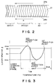
- a smectic liquid crystal generally has a layer structure, of which the smectic layer thickness (generally called “layer spacing” in the art and the term “layer spacing” is also used herein) shrinks or decreases on transition from SmA phase to SmC phase or SmC* phase, so that the liquid crystal assumes a chevron structure as shown in Figure 2, in which the liquid crystal or smectic layers 21 are bent at a mid point between the substrate surfaces 24a and 24b.
- layer spacing the smectic layer thickness
- the bending can occur in two directions, i.e., one in an alignment state 22 (C1 alignment state) which appears immediately after transition into SmC* from a higher temperature phase and the other in another alignment state 23 (C2 alignment state) appearing on further temperature decrease in mixture with the C1 alignment state.
- C1 alignment state an alignment state 22
- C2 alignment state another alignment state 23
- the directors of liquid crystal molecules in the C1 alignment state and the C2 alignment state are disposed on cones 31 as shown in Figures 1A and 1B in the vicinity of a substrate surface.
- a liquid crystal molecule on a rubbed substrate surface raises its head in the direction A to form an angle ⁇ (called a "pretilt (angle)") with respect to the substrate surface.
- condition of formula (3) (i.e., ⁇ > ⁇ ) is given as a condition for easy switching from one orientation state to the other of a liquid crystal molecule at the substrate surface under application of an electric field.
- the formula (3) should be satisfied in addition to the formula (2).
- a ferroelectric liquid crystal has potentially very excellent characteristics and has provided essential improvements to many of the problems encountered in conventional TN-liquid crystal devices, in combination with the conditions for adapting the liquid crystal molecular states to the device structures as described above. As a result, it is expected to be utilized in high-speed optical shutters and high-density, large area displays exceeding conventional TN-type liquid crystal displays and CRT displays.
- a display apparatus may be constituted by a display panel comprising scanning electrodes and data electrodes arranged in a matrix, and drive means including means for selecting all or a prescribed number of scanning electrodes for so-called whole-area writing and means for selecting a part of the all or a prescribed number of scanning electrodes for a so-called partial writing, so that a partial motion picture display may be effected by the partial writing, and the partial writing and the whole-area writing are compromised.
- a large-area, high resolution display can be driven to provide high-contrast images at a high speed by driving a liquid crystal device (panel) in the above-mentioned display apparatus adapted for partial writing.
- the environmental temperature surrounding the liquid crystal device can be expanded to ca. 5 - 50 o C because of accumulation of heat evolved from the device per se.
- An ordinary ferroelectric liquid crystal generally causes a remarkably large temperature-dependent change in response speed because the response speed largely depends on the viscosity thereof so that the change in response speed reaches ten and several times corresponding to a temperature change in the range of 5 - 50 o C. This exceeds a controllable limit attainably by control of drive voltage, etc.
- an identical image display should be performed under identical conditions over a planar temperature distribution of several degrees to ten and several degrees, but liquid crystal materials available at present have a large temperature dependence of drive conditions and are not sufficient for such a commercial use.
- an available liquid crystal material can be accompanied with a difficulty that, when it is heated or cooled in excess of an ordinary operational temperature range for, e.g., display and then cooled or heated to the ordinary operational temperature range, it can show drive characteristics which are different from those before the heating or cooling.
- an object of the present invention is to provide a liquid crystal composition having improved temperature-dependence of characteristics, such as response speed and alignment state, over a wide temperature range including room temperature region.
- Another object of the present invention is to provide a liquid crystal device including such a liquid crystal composition in a stable alignment state and having drive conditions which are little dependent on temperature and include a high response speed and a good contrast over an operational temperature range.
- a further object of the present invention is to provide a liquid crystal apparatus including such a liquid crystal device.
- a liquid crystal composition successively assuming SmA (smectic A) phase and SmC* (chiral smectic) phase on temperature decrease, said liquid crystal composition having a temperature-dependence of layer spacing d in smectic phase such that the layer spacing d increases, is constant or decreases on temperature decrease in SmA phase temperature range, assumes a first transition point where the layer spacing d abruptly decreases on temperature decrease in vicinity of transition temperature from SmA phase to SmC* phase, and assumes a second transition point where the layer spacing d commences to increase on further temperature decrease below the first transition point in SmC* temperature range.
- a liquid crystal device comprising a liquid crystal composition as described above between a pair of substrates.
- a liquid crystal apparatus including a liquid crystal device as described above and drive means therefor.
- Figures 1A and 1B are illustrations of relationships among cone angle H , pretilt angle ⁇ and layer inclination angle ⁇ in C1 alignment and C2 alignment, respectively.
- Figure 2 is an illustration of a chevron layer structure including a C1 alignment portion and a C2 alignment portion.
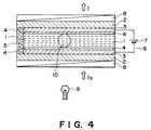
- Figure 3 is a graph showing an example of temperature-dependent layer spacing-changing characteristic in SmC* phase.
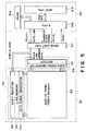
- Figure 4 is ia sectional view of an embodiment of a liquid crystal device according to the invention.
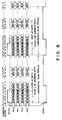
- Figure 5 is a block diagram of a liquid crystal apparatus according to the invention and a graphic controller.
- Figure 6 is a time chart showing time correlation for image data communication between the liquid crystal apparatus and the graphic controller.
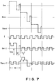
- Figure 7 is a time chart showing a set of drive voltage waveform for measuring a drive margin.
- Figure 8 is an illustration of an instrument system including an X-ray diffraction system and an automatic temperature controller for measuring a layer spacing d in smectic phase of a liquid crystal composition.
- Figure 9 is an illustration of a drive margin.
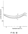
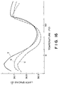
- Figures 10 - 16 are respectively a graph showing a temperature-dependent layer spacing-changing in smectic phase of a liquid crystal composition or liquid crystal compositions used in Examples.
- a liquid crystal composition in a liquid crystal composition, particularly a ferroelectric liquid crystal composition having SmC* phase, a liquid crystal composition can have a remarkably different temperature-dependence of response speed, particularly at a low temperature side in some cases, by changing a component liquid crystal compound with a similar compound having a slightly different side chain length, even if the viscosity coefficient and spontaneous polarization are not substantially changed.
- This phenomenon may be attributable to the temperature-dependence of the inclination angle of liquid crystal molecules and the layer spacing in the neighborhood of a temperature at which the temperature-dependence of response speed differs.
- liquid crystal device containing a liquid crystal composition having the above-mentioned characteristic or liquid crystal display apparatus including such a liquid crystal device is heated to the SmA phase temperature range of the composition in excess of an ordinary operational temperature range and then cooled again to the ordinary operation temperature range, the display characteristics, such as contrast and display speed, can be different from those before the heating.
- a liquid crystal composition particularly one assuming a chevron-structured liquid crystal phase, with a suppressed change in structural parameters accompanying the phase transition and a particularly improved temperature-dependence of response speed over a wide temperature range by selecting a liquid crystal composition which causes a successive phase transition from SmA phase to SmC* phase on temperature decrease, has a first transition point (temperature) where the layer spacing d decreases abruptly, e.g., discontinuously in the vicinity of the SmA to SmC* phase transition temperature, and also has a second transition point (temperature) where the layer spacing d further decreases and turns to increase on further temperature decrease in the SmC* temperature range.
- a liquid crystal composition can provide a liquid crystal device, such as a liquid crystal display device, showing improved temperature characteristics, such as contrast.
- the liquid crystal composition according to the present invention may preferably have a smectic layer spacing d in SmA which increases or is constant on temperature decrease so as to provide improved high temperature characteristics and particularly a further stabilized liquid crystal alignment state even when heated to the SmA phase temperature range and stored at a higher temperature exceeding the SmC* temperature range, thus providing characteristics with good reproducibility at normal temperature.
- the liquid crystal composition according to the present invention may preferably have a layer spacing-changing characteristic that it has a layer spacing d A at the first transition point and a layer spacing d min at the second transition point satisfying: 0.966 ⁇ d min /d A (7), more preferably 0.976 ⁇ d min /d A ⁇ 0.990 (8).
- d at the SmA ⁇ SmC* transition temperature is taken as d A .
- the liquid crystal composition according to the present invention successively assumes SmA phase and SmC* phase, has a layer spacing d in smectic phase which increase, decreases or is constant on temperature decrease in SmA phase, has a first transition point where d abruptly decreases on temperature decrease in the vicinity of a transition point from SmA to SmC*, a second transition point where d turns to increase in SmC* phase on further temperature decrease after passing the first transition point and further a third transition point where d again turns to decrease on a low temperature side than the second transition point.
- a liquid crystal composition having such a temperature-dependent layer spacing-changing characteristic including a third transition point may have further improved temperature characteristics, such as temperature-dependence of response speed, on a low temperature side, and stable characteristics, such as response speed, contrast and alignment state, after storage at a low temperature.
- the layer spacing d min at the second transition point and the layer spacing d A at the first transition point may preferably satisfy 0.966 ⁇ d min /d A (7) , more preferably 0.978 ⁇ d min /d A (9) in case where the third transition point exhibits.
- the liquid crystal composition may preferably have the second transition point in SmC* phase in the temperature range of 20 - 50 o C, more preferably 30 - 50 o C.
- the liquid crystal composition may preferably have a temperature-dependence of layer spacing d such that it assumes a minimum layer spacing d c in a range from the third transition point to the phase transition temperature to a lower temperature phase than SmC* which satisfies the following relationship with the layer spacing d A at the first transition point: d c /d A ⁇ 1.033 (10).
- d at the phase transition temperature is taken as d A .
- the liquid crystal composition may preferably have a layer spacing d max at the third transition temperature which satisfies the following relationship with the layer spacing d A at the first transition point: 0.993 ⁇ d max /d A ⁇ 1.003 (11).
- the liquid crystal composition may preferably satisfy the formula (7), more preferably the formula (9), between d min and d A and have the second transition point providing d min within the range of 20 - 50 o C, more preferably 30 - 50 o C, in order to provide a liquid crystal device with little temperature-dependence of response speed and higher-speed drive characteristic.
- the liquid crystal composition having a layer spacing-changing characteristic according to the present invention may have a temperature characteristic of cone angle H in SmC* phase such that H increases on temperature decrease in SmC* temperature range and assumes a maximum H max at a transition point below which H turns to decrease.
- the layer spacing d can exceed the layer spacing d A at the first transition on a lower temperature side in the SmC* phase in some cases.
- Td B a temperature at which d reaches d A
- the liquid crystal cannot recover the original characteristics, such as the alignment state, apparent tilt angle ⁇ a, contrast and response speed even when it is reheated to an operational temperature for display in some cases. This can pose a serious problem for storage or use of a liquid crystal composition or a liquid crystal device.
- a liquid crystal composition can be stably present in a super-cooled state when it is contained in a cell, so that it does not cause crystallization or local crystallization even below its melting point in the bulk state.
- the lower limit temperature for storage may be determined by the above-mentioned Td B rather than the melting point.
- Figure 3 shows an example of a temperature-dependence of layer spacing d of a liquid crystal composition having such first, second and third transition points. Based on such a temperature characteristic, the characteristics, such as response speed and display contrast of a liquid crystal composition, can be further improved by adjusting the relationship among d A , d min , d c and d max and the change of d between the first and second transition points, and between the second and third transition points.
- the liquid crystal composition according to the present invention comprises at leas one mesomorphic compound and is provided with SmA phase and SmC* phase and the above-mentioned smectic layer spacing-changing characteristic having the first and second transition points by adjusting the mesogen groups and combination thereof for providing skeleton structures, kinds and lengths of side chains, and compositional ratios among the components. More specifically, the liquid crystal composition may comprise at least one mesomorphic compound, such as phenylpyrimidine compounds and thiazole compounds.
- indan compounds represented by the following formula (A): wherein R1 and R2 independently denote a linear or branched alkyl group having 1 - 18 carbon atoms; X1 and X2 independently denote a single bond, -O-, -CO ⁇ O-, or -O ⁇ CO-; A1 denotes a single bond,
- the liquid crystal composition may preferably contain at least one species of quinoxaline compounds represented by the following formula (B) in addition to the indan compound of the formula (A): wherein R3 and R4 independently, denote a linear or branched alkyl grope having 1 - 18 carbon atoms; X3 denotes a single bond, -O-, -CO ⁇ O- or -O ⁇ CO-; and A3 denotes
- a coumaran compound represented by the formula (C) in addition to the indan compound of the formula (A): wherein R5 and R6 independently denote a linear or branched alkyl group having 1 - 18 carbon atoms; X4 and X5 independently denote a single bond, -O-, -CO ⁇ O- or -O ⁇ CO-; A4 denotes a single bond,
- the liquid crystal composition according to the present invention may preferably contain at least one species each of the indan compound of the formula (A), the quinoxaline compound of the formula (B) and/or the coumaran compound of the formula (C) in a proportion of 1 - 30 wt. %, preferably 5 - 30 wt. %, further preferably 8 - 25 wt. %, respectively.
- D mesomorphic compounds
- A6 denotes X6 denotes hydrogen or fluoride
- C1 denotes Z denotes -O- or -S-;
- Preferred structural examples of the compounds of the formulae (D) - (G) may include those enumerated hereinbelow.
- the mesomorphic compounds represented by the formulae (D) - (H) constitute in total at least 30 wt. %, more preferably 50 - 90 wt. %, of the liquid crystal composition according to the present invention.
- Figure 4 is a schematic sectional view of an embodiment of the liquid crystal device using a chiral smectic liquid crystal layer for describing a structure of the liquid crystal device utilizing ferroelectricity.
- the liquid crystal device includes a chiral smectic liquid crystal layer 1 disposed between a pair of glass substrates 2 each having thereon a transparent electrode 3 and an alignment control layer 4.
- Lead wires 6 are connected to the electrodes 3 so as to apply a driving voltage to the liquid crystal layer 1 from a power supply 7.
- a pair of polarizers 8 are disposed so as to modulate incident light I0 from a light source 9 in cooperation with the liquid crystal 1 to provide modulated light I.
- Each of two glass substrates 2 is coated with a transparent electrode 3 comprising a film of In2O3, SnO2 or ITO (indium-tin-oxide) to form an electrode plate.
- a transparent electrode 3 comprising a film of In2O3, SnO2 or ITO (indium-tin-oxide) to form an electrode plate.
- an alignment control layer 4 is formed by rubbing a film of a polymer such as polyimide with gauze or acetate fiber-planted cloth so as to align the liquid crystal molecules in the rubbing direction.
- the alignment control layer from an insulating material including an inorganic material, such as silicon nitride, silicon nitride containing hydrogen, silicon carbide, silicon carbide containing hydrogen, silicon oxide, boron nitride, boron nitride containing hydrogen, cerium oxide, aluminum oxide, zirconium oxide, titanium oxide, or magnesium fluoride, and also an organic insulating material, such as polyvinyl alcohol, polyimide, polyamide-imide, polyester-imide, polyparaxylylene, polyester, polycarbonate, polyvinyl acetal, polyvinyl chloride, polyvinyl acetate, polyamide, polystyrene, cellulose resin, melamine resin, urea resin, acrylic resin, or photoresist resin.
- an inorganic material such as silicon nitride, silicon nitride containing hydrogen, silicon carbide, silicon carbide containing hydrogen, silicon oxide, boron nitride, boron nitride containing
- Such an alignment control layer can be composed of two layers. Alternatively, it is also possible to use a single layer of inorganic insulating alignment control layer or organic insulating alignment control layer.
- An inorganic alignment control layer may be formed by vapor deposition, while an organic alignment control layer may be formed by applying a solution of an organic insulating material or a precursor thereof in a concentration of 0.1 to 20 wt. %, preferably 0.2 - 10 wt. %, by spinner coating, dip coating, screen printing, spray coating or roller coating, followed by curing or hardening under prescribed hardening condition (e.g., by heating).
- the inorganic insulating layer may have a thickness of ordinarily 30 ⁇ - 1 ⁇ m, preferably 40 - 3000 ⁇ , further preferably 40 - 1000 ⁇ .
- the two glass substrates 2 with transparent electrodes 3 and further with alignment control layers 4 thereof are held to have a prescribed (but arbitrary) gap with a spacer 10 and a sealing member 5.
- a cell structure with a prescribed gap may be formed by sandwiching spacers 10 of silica beads or alumina beads having a prescribed diameter with two glass plates, and then sealing the periphery thereof with an sealing member 5 of, e.g., an epoxy adhesive.
- a polymer film or glass fiber may also be used as a spacer.
- a chiral smectic liquid crystal is sealed up to provide a liquid crystal layer in a thickness of generally 0.5 to 20 ⁇ m, preferably 1 to 5 ⁇ m.
- the liquid crystal 1 has an SmC* phase (chiral smectic C phase) in a broad temperature range including room temperature, particular at a lower temperature side thereof, and provides a device showing a broad drive voltage margin and a broad drive temperature margin.
- SmC* phase chiral smectic C phase
- the liquid crystal has a phase transition series of isotropic - Ch (cholesteric) phase - SmA (smectic A) phase - SmC* (chiral smectic C) phase.
- the transparent electrodes 3 are connected to the external power supply 7 through the lead wires 6. Further, outside the glass substrates 2, polarizers 8 are applied. Behind the polarizer 8 is disposed optionally a light source 9.
- the liquid crystal device according to the present invention may be provided with improved characteristics inclusive of a contrast by appropriately adjusting the device manufacturing conditions, such as a cell gap (liquid crystal layer thickness) between the substrates, and materials and rubbing conditions for the alignment control layer in combination with the liquid crystal composition according to the invention so as to satisfy the above-mentioned formulae (2), (3) and (4).
- the device manufacturing conditions such as a cell gap (liquid crystal layer thickness) between the substrates, and materials and rubbing conditions for the alignment control layer in combination with the liquid crystal composition according to the invention so as to satisfy the above-mentioned formulae (2), (3) and (4).
- liquid crystal device having a structure similar to that shown in Figure 4 was prepared in the following manner.
- Two 1.1 mm-thick glass plates as substrates 2 were respectively provided with transparent tripe electrodes 3 of ITO (indium tin oxide) together with side metal electrodes (not shown) of molybdenum and was further coated thereon with a 1500 ⁇ -thick transparent dielectric film of tantalum oxide (not shown) by sputtering.
- ITO indium tin oxide
- side metal electrodes not shown
- molybdenum molybdenum
- an NMP solution of a polyimide precursor (e.g., "LQ-1802", mfd. by Hitachi Kasei K.K.; “LP-64” mfd. by Toray K.K., and "RN-305" mfd. by Nissan Kagaku K.K.) was applied by a printing method and baked at 200 - 270 o C to form a 100 to 300 ⁇ -thick polyimide alignment control film 4. After the baking, the film 4 was rubbed with an acetate fiber yarn-planted cloth. The pretilt angle may be controlled by appropriately selecting and combining the rubbing intensity governed by the rubbing cloth rotation speed and substrate feed speed and the polyimide alignment film materials.
- a polyimide precursor e.g., "LQ-1802", mfd. by Hitachi Kasei K.K.; "LP-64” mfd. by Toray K.K., and "RN-305" mfd. by Nissan Kagaku K.K.
- the two substrates were treated in the above-described manner.
- epoxy resin adhesive particles having an average particle size of 5.5 ⁇ m (“Toraypearl” mfd. by Toray K.K.) were dispersed at a density of 50 particles/mm2 according to the Nordson electrostatic dispersion scheme.
- silica microbeads having na average particle size of 1.2 ⁇ m was dispersed as spacers 10 at a density of 300 particles/mm2 by the Nordson electrostatic dispersion scheme.
- a liquid epoxy adhesive (“STRUCT BOND”, mfd.
- the cell was evacuated to a reduced pressure of 10 ⁇ 4 atm and filled with a ferroelectric liquid crystal composition heated to its isotropic phase to provide a liquid crystal cell.
- the liquid crystal cell thus prepared may be sandwiched between a pair of polarizers 8 and driven by application of drive voltages from an external voltage supply 7 as illustrates in Figure 4.
- a liquid crystal device may preferably be used to constitute a display apparatus in combination with a drive circuit and a light source.
- a liquid crystal display apparatus may be constituted by using the liquid crystal device for a display panel and by adopting an arrangement and data format comprising image data accompanied with scanning line address data and also a communication synchronization scheme using a SYNC signal as shown in Figures 5 and 6.
- Image data are generated in a graphic controller 52 in an apparatus body and transferred to the display panel 53 (illuminated with a backlight (not shown)) by signal transfer means shown in Figures 5 and 6.
- the graphic controller 52 principally comprises a CPU (or GCPU, central processing unit) 512 and a VRAM (video-RAM, image data storage memory) 514 and is in charge of management and communication of image data between a host CPU 513 and the liquid crystal display apparatus (FLCD) 51.
- the control of image display according to the present invention is principally accomplished by the graphic controller 52.
- FIG. 7 is a waveform diagram showing a set of drive waveforms for effecting image display on the display panel wherein at S N and S N+1 are shown voltage waveforms applied to scanning electrodes S N and S N+1 , and at I is shown a voltage waveform applied to a data electrode I, whereby voltages as shown at S N - I and S N+1 - I are applied to pixels at the intersections of the scanning electrodes and the data electrode.
- liquid crystal compositions were evaluated by incorporating them in liquid crystal devices having a structure similar to that described with reference to Figure 4 and prepared in a process similar to the one described above.
- response speed cone angle H apparent tilt angle ⁇ a
- liquid crystal layer inclination angle ⁇ liquid crystal layer inclination angle ⁇
- pretilt angle ⁇ smectic layer spacing d
- a sample device sandwiched between right-angle cross-nicol polarizers was supplied with rectangular pulse waves of ⁇ 10.0 volts and 5.0 Hz, and a time required for causing a light quantity change of 0 to 90 % was measured as a response time ⁇ representing a response speed while observing the optical response through a photomultiplier (available from Hamamatsu Photonics K.K.).
- a sample liquid crystal device was sandwiched between right angle-cross nicol polarizers and rotated horizontally relative to the polarizers under application of an AC voltage of ⁇ 30 V to ⁇ 50 V and 100 Hz between the upper and lower substrates of the device while measuring a transmittance through the device by a photomultiplier (available from Hamamatsu Photonics K.K.) to find a first extinct position (a position providing the lowest transmittance) and a second extinct position.
- a cone angle H was measured as a half of the angle between the first and second extinct positions.
- a sample device sandwiched between right angle cross nicol polarizes was supplied with a single pulse of one polarity exceeding the threshold voltage of the ferroelectric liquid crystal and was then rotated under no electric field horizontally relative to the polarizers to find a first extinction position. Then, the device was supplied with a single pulse of the opposite polarity exceeding the threshold voltage of the liquid crystal and was then rotated under no electric field relative to the polarizers to find a second extinct position.
- An apparent tilt angle ⁇ a was measured as a half of the angle between the first and second extinct positions.
- the methods used were basically similar to the method used by Clark and Lagerwall (Japan Display '86, Sept. 30 - Oct. 2, 1986, p.p. 456 - 458) or the method of Ohuchi et al (J.J.A.P., 27 (5) (1988), p.p. 725 - 728).
- the measurement was performed by using a diffraction apparatus (available from MAC Science having a rotary cathode-type X-ray generating unit as shown in Figure 8), and 80 ⁇ m-thick glass sheets ("Microsheets", available from Corning Glass Works) were used as substrates so as to minimize the heat capacity and the X-ray absorption with the glass substrates.
- a system as shown in Figure 8 was used, wherein a sample liquid crystal composition 801 was applied in a 5 mm-square size so as to form a flat surface on the 80 ⁇ m-thick glass sheet and, while being temperature-controlled by a temperature-controlling plate 805 and a temperature-monitoring thermocouple 806, irradiated with X rays from a rotary X-ray source 802, so that the output light including diffraction rays was detected by a detector (counter) 803, similarly as in the ordinary powder X-ray diffraction. An angle providing a peak of X-ray intensity was substituted in the Bragg's formula for diffraction condition to obtain a layer spacing d .
- Each sample liquid crystal composition was first brought to its isotropic phase temperature, and the measurement was repeated every 5 o C or every 1 o C in the vicinity of a transition point while cooling the sample down to a temperature where no diffraction peak was observed.
- the automatic temperature controller including the plate 805 and the monitoring thermocouple 804 allowed a control accuracy of ⁇ 0.3 o C at each measurement temperature.
- the measurement was performed by using CuK ⁇ -rays (1.54050 ⁇ ) at a power of 45 kV-100 mA as analyzing rays and using a slit system including DS of 0.05 mm, SS of 0.05 mm and RS of 0.05 mm. The scanning was performed at a rate of 3 deg./min.
- a sample cell having a cell gap of 80 ⁇ m was prepared by using a pair of the 80 ⁇ m-thick glass sheets while using the same glass sheet as a spacer.
- a sample liquid crystal composition filling the sample cell was heated to isotropic phase and then gradually cooled to be homogeneously aligned under application of a magnetic field in a direction parallel to the substrates by an electromagnet.
- the X-ray detector was set at the angle 2 ⁇ giving the above-mentioned layer spacing d , and the sample cell was subjected to ⁇ -scanning. From the measured values, ⁇ was calculated according to the method described in the above-mentioned references.
- a pair of substrates rubbed in mutually parallel and opposite directions were applied to each other to form a cell having a cell gap of 20 ⁇ m, which was then filled with a liquid crystal mixture assuming SmA phase in the temperature range of 10 - 55 o C obtained by mixing 80 wt. % of a ferroelectric liquid crystal ("CS-1014", mfd. by Chisso K.K.) with 20 wt. % of a compound represented by the following formula:
- the liquid crystal cell was rotated in a plane perpendicular to the pair of substrates and including the aligning treatment axis and, during the rotation, the cell was illuminated with a helium-neon laser beam having a polarization plane forming an angle of 45 degrees with respect to the rotation plane in a direction normal to the rotation plane, whereby the intensity of the transmitted light was measured by a photodiode from the opposite side through a polarizer having a transmission axis parallel to the polarization plane.
- a sample liquid crystal device disposed between right-angle cross-nicol polarizers was supplied with a single pulse of one polarity to uniformly form one stable state and then rotated relative to the polarizers to find a first extinction position.
- the liquid crystal device fixed at the position was then supplied with a single pulse of the opposite polarity to form another stable state giving a bright state at the observed position.
- the output voltage from a photomultiplier in this state is divided by the output voltage in the extinction position to provide a contrast.
- Electrodes on a pair of substrates of a sample liquid crystal device disposed between a pair of right-angle cross-nicol polarizers were supplied with a combination of a scanning signal, e.g., as shown at S N and a data signal, e.g., as shown at I in Figure 7 so as to write a dark state and a bright state, respectively while varying a pulse duration T at a fixed peak value Vop allowable ranges of T for stably providing a dark state and a bright state were measured.
- the drive margin M has a larger value if a larger overlapping of the ranges T1 and T2 for writing dark and bright states is obtained.
- phase transition temperatures of each liquid crystal composition were measured by a DSC (differential scanning calorimeter) in combination with an observation of a cell containing the liquid crystal composition through a polarizing microscope.
- Table 4 below shows phase transition temperatures ( o C, on temperature decrease), SmA phase temperature range width ( o C) and types of temperature-dependent layer spacing d -changing characteristic for liquid crystal compositions A - K and other commercially available compositions ("CS-1017", available from Chisso K.K.; and "ZLI-3233" available from Merck Co.) used in Examples 1 - 20 appearing hereinafter.
- the temperature-dependent layer spacing-changing characteristics are also shown in Figures 10 - 12.
- the temperature-dependent layer spacing d -changing characteristics shown in Table 4 are characterized by types I - V according to the following standards:
- liquid crystal compositions A - H shown in Table 4 are all compositions comprising a phenylpyrimidine-type mesomorphic compound as a principal component.
- liquid crystal compositions I, J and K include the component compounds identified by their structural formulae shown below in the respectively indicated proportions:
- Each device was prepared by using "LQ-1802" for alignment control films so as to provide a pretilt angle of ca. 17 deg., a rubbing intersection angle of 8 deg., and a cell gap of 1.2 ⁇ m.
- the liquid crystal compositions CS-1017 and ZLI-3233 having no minimum (second transition point) of layer spacing in SmC* phase showed temperature characteristic factor f 10/50 regarding response speed (a ratio of response time between 10 o C and 50 o C) which were 15 or larger in an expected environmental temperature range of 10 - 50 o C for a liquid crystal display device.
- the liquid crystal compositions A, D and F having a minimum (second transition point) of layer spacing in SmC* phase showed temperature characteristic factors f 10/50 on the order of 3 - 4 indicating an improved temperature-dependence of response speed.
- liquid crystal compositions all having a minimum (second transition point) of liquid crystal in SmC* phase including some compositions (A, C, D and F) of which the layer spacing increased or was constant on temperature decrease in SmA phase and other compositions (B and E) of which the layer spacing decreased on temperature decrease in SmA phase, were examined with respect to a contrast change before and after a temperature increase spanning the phase transition temperature of SmC* phase to SmA phase.
- Table 6 The results are shown in Table 6.
- each liquid crystal device was prepared by using "LQ-1802" for alignment control films so as to provide a pretilt angle of ca. 19 degrees, a rubbing intersection angle of 6 degrees, and a cell gap of 1.1 ⁇ m.
- Each liquid crystal device prepared was heated from room temperature at a rate of 1 o C/min. up to a temperature which was 5 o C above the SmC* ⁇ SmA transition temperature and retained for 10 hours at that temperature, followed by cooling to room temperature at a rate of 1 o C/min.
- the contrast of each device was measured at 30 o C respectively before and after the heating.
- liquid crystal compositions A, C, D and F having a minimum (second transition point) of layer spacing in SmC* and also a layer spacing increasing or being constant in SmA phase showed much less contrast change before and after heating over the SmC* ⁇ SmA phase transition temperature, compared with the liquid crystal compositions B and E having a layer spacing which decreased on temperature decrease in SmA phase.
- such compositions A, C, D and F caused little change in alignment state even under heating over the phase transition temperature and were estimated to show stable characteristics, particularly stable display characteristics, even after a storage at higher temperatures.
- compositions having a minimum d min (second transition point) of layer spacing in SmC* phase compositions satisfying and not satisfying the following formula (8) between d min and d A (layer spacing at a first transition point in the vicinity of the SmA ⁇ SmC* phase transition temperature) were evaluated with respect to drive margin: 0.975 ⁇ d min /d A ⁇ 0.990 (8).
- Table 7 The results are shown in Table 7.
- Each device was prepared by using "LQ-1802" for alignment control films so as to provide a pretilt angle of ca. 16 degrees, a rubbing intersection angle of 8 degrees, and a cell gap of 1.2 ⁇ m.
- the drive margin was measured while setting the writing peak voltage Vop at 15 volts (in the waveform shown in Figure 7).
- Each device was prepared by using "LQ-1802" for alignment control films so as to provide a pretilt angle of ca. 18 degrees, a rubbing intersection angle of 8 degrees, and a cell gap of 1.2 ⁇ m.
- composition I of Example 18 showing Type I of temperature-dependent layer spacing-changing characteristic in SmC* phase, showed a much smaller temperature-dependence of response speed.
- composition J and K containing both indan compound and quinoxaline compound also showed Type I of temperature-dependence layer spacing-changing characteristic and further smaller temperature-dependence of response speed. This tendency was also confirmed with respect to other compositions containing both indan compound and quinoxaline compound, which were thus regarded to be suitable as liquid crystal compositions showing the characteristics required by the present invention.
- Table 9 below shows phase transition temperatures (generally, on temperature decrease) and Table 10 below shows types of temperature-dependent layer spacing d -changing characteristics in smectic phase and characteristic ratios d min /d A , d max /d A and d c /d A (wherein d A : layer spacing at the first transition point, d max : layer spacing at the third transition point; d min : layer spacing at the second transition point; and d c : a minimum value of layer spacing below the third transition point in SmC* phase down to another lower-temperature), respectively, of liquid crystal compositions L - V and commercially available composition "CS-1017" and "ZLI-3233".
- the temperature-dependent layer spacing d -characteristics are also shown in Figures 13 - 16.
- the temperature-dependent layer spacing d-changing characteristics shown in Table 10 are characterize by types VI - IX according to the following standards:
- liquid crystal compositions L, N, P, Q, R and S in Tables 9 and 10 are all compositions comprising a phenylpyrimidine-type mesomorphic compound as a principal component.
- liquid crystal compositions M, O, T, U and V have the following compositions.
- Each liquid crystal device was prepared to have a structure similar to the one described with reference to Figure 4 similarly as those used in Examples 1 - 20. More specifically, each device was prepared in the following manner.
- Two 0.7 mm-thick glass sheets as substrates were coated with ITO films and further with insulating films. Each substrate was further coated with a polyimide resin precursor, followed by baking and rubbing with an acetate fiber yarn-planted cloth. Then, two substrates were applied to each other so as to form a cell gap of ca. 1.5 ⁇ m, which was then filled with a sample liquid crystal composition in isotropic phase or cholesteric phase, followed by gradual cooling to room temperature to provide a liquid crystal device.
- Each liquid crystal device was subjected to measurement of response speed (response time) and the temperature dependence thereof was evaluated in terms of a temperature characteristic factor f 10/40 (a ratio of response time between 10 o C and 40 o C). A smaller value of f 10/40 represents a better temperature dependence of response speed.
- Two 1.1 mm-thick glass plates as substrates were respectively provided with transparent tripe electrodes of ITO (indium tin oxide) together with side metal electrodes of molybdenum and was further coated thereon with a 1500 ⁇ -thick transparent dielectric film of tantalum oxide (not shown) by sputtering.
- ITO indium tin oxide
- an NMP solution of a polyimide precursor ("LQ-1802", mfd. by Hitachi Kasei K.K.) was applied by a printing method and baked at 270 o C to form a 300 ⁇ -thick polyimide alignment control film. After the baking, the film was rubbed with an acetate fiber yarn-planted cloth.
- the two substrates were treated in the above-described manner.
- epoxy resin adhesive particles having an average particle size of 5.5 ⁇ m (“Toraypearl” mfd. by Toray K.K.) were dispersed at a density of 50 particles/mm2 according to the Nordson electrostatic dispersion scheme.
- silica microbeads having an average particle size of 1.5 ⁇ m were dispersed at a density of 300 particles/mm2 by the Nordson electrostatic dispersion scheme.
- a liquid epoxy adhesive (“STRUCT BOND”, mfd. by Mitsui Toatsu Kagaku K.K.) was applied by printing in a thickness of 6 ⁇ m.
- the two substrates were applied to each other so that their rubbing directions were dispose in almost identical directions but with an anticlockwise intersection angle of 8 degrees and press-bonded to each other under a pressure of 2.8 kg/cm2 for 5 min. at 70 o C, followed by heating at 150 o C under a pressure of 0.63 kg/cm2 for 4 hours to cure the two types of adhesives, thereby preparing a blank cell.
- the cell was evacuated to a reduced pressure of 10 Pa and filled with a sample liquid crystal composition heated to its isotropic phase to provide a liquid crystal device (panel).
- Each liquid crystal device (panel) had a picture area defined by a lateral size of ca. 280 mm (data line side) and a vertical size of ca. 220 mm (scanning line side) providing 1280 x 1024 pixels.
- the respective sample liquid crystal panels were placed in a large-sized thermostatic vessel and cooled from room temperature at a rate of 1 o C/min. to -25 o C while controlling the temperature so as to provide a substantially uniform temperature over the entire panel face, followed by standing for 5 hours at -25 o C and temperature-raising to room temperature at a rate of 3 o C/min. Then, the alignment state and response speed of each sample panel were measured and compared with those before the low-temperature storage.
- the liquid crystal compositions L, M and N having Type VII of layer spacing-changing characteristic showed worse display performances, such as a decrease in ⁇ a resulting in a lower contrast and a change in response speed, after the low-temperature storage.
- liquid crystal compositions O, P and Q having Type VIII or IX of layer spacing-changing characteristic showed substantially no change after 5 hours of low-temperature storage. Accordingly, it is suggested that a liquid crystal composition having a third transition point shows a stable performance even after low temperature storage.
- Liquid crystal compositions used were those having Type VII, VIII or IX of layer spacing-changing characteristic.
- Each sample panel was placed in a thermostatic vessel and cooled from room temperature at a rate of 1 o C/min. to -10 o C or -25 o C while effecting a temperature control so as to provide a uniform temperature over the entire panel face, followed by standing at -10 o C or -25 o C for 120 hours and temperature raising to room temperature at a rate of 3 o C/min or 3 o C/hour. Then, the alignment state and response speed of each sample panel were measured and compared with those before the low-temperature storage.
- the liquid crystal compositions Q, R and S having Type IX of layer spacing-changing characteristic showed no change in alignment state even after low-temperature storage under any conditions. Further, among the liquid crystal compositions N and O having Type VIII of layer spacing-changing characteristic, the composition N showed no change in alignment state or response speed after a storage at -10 o C where d did not exceed d A .
- the liquid crystal compositions having Type VIII of layer spacing-changing characteristic caused a decrease in ⁇ a after a storage at a temperature (-25 o C) causing d to exceed d A in some cases but the composition O was substantially free from a change in display characteristic after storage at -25 o C in case where the panel was warmed at a higher rate of 3 o C/min.
- the effect of low-temperature storage could be different depending on a complex combination of factors, such as storage temperature, time and temperature-changing rate and could not be simply determined based on the storage temperature alone.
- a liquid crystal composition having a d max /d A ratio smaller than 0.993 is liable to cause a slower response speed at low temperatures, thus making it difficult to effect a uniform image over a large-area panel over a wide temperature range.
- the liquid crystal composition M contains none of indan compound or coumaran compound.
- the liquid crystal composition T contains 17 % of an indan compound;
- the composition U contains 17 % of an indan compound and 6 % of a coumaran compound;
- the composition V contains 17 % of an indan compound and totally 5 % of two coumaran compounds.
- the compositions M, T, U and V showed Types VII, VIII, IX and IX, respectively, of layer spacing-changing characteristic, thus suggesting that the inclusion of both indan and coumaran compounds provided compositions (U and V) which were expected to show excellent low-temperature storage durability (Type IX of layer spacing-changing characteristic).
- composition U and V having Type IX of layer spacing-changing characteristic by inclusion of both indan and coumaran compounds caused no charge in display characteristics after the low temperature storage.
- the liquid crystal composition according to the present invention has been provided with improved temperature-dependence of performances including a response speed and sufficient drive margin over an expected operational temperature range in a liquid crystal device, particularly a display device. Further, if the layer spacing d changing characteristic in SmA phase is adjusted, the composition is provided with a suppressed change in drive characteristic at high temperatures and provides a high contrast even after a storage at high temperatures. Further, if the layer spacing d -changing characteristic in SmC* phase is further adjusted, the composition is provided with further improved low-temperature performances and provides a very stable alignment state even after storage at low temperatures. Accordingly, by using the liquid crystal composition and the liquid crystal device including the composition according to the present invention, it is possible to provide a liquid crystal apparatus, particularly a liquid crystal display apparatus, capable of exhibiting excellent display performances.
- a liquid crystal device with little temperature-dependence of drive characteristics, such as response speed, and with good storage stability, can be produced by using a liquid crystal composition, successively assuming SmA (smectic A) phase and SmC* (chiral smectic) phase on temperature decrease.
- the layer spacing composition has a temperature-dependence of layer spacing d in smectic phase such that the layer spacing d increases, is constant or decreases on temperature decrease in SmA phase temperature range, assumes a first transition point where the layer spacing d abruptly decreases on temperature decrease in vicinity of transition temperature from SmA phase to SmC* phase, and assumes a second transition point where the layer spacing d commences to increase on further temperature decrease below the first transition point in SmC* temperature range.
Landscapes
- Chemical & Material Sciences (AREA)
- Crystallography & Structural Chemistry (AREA)
- Engineering & Computer Science (AREA)
- Materials Engineering (AREA)
- Organic Chemistry (AREA)
- Liquid Crystal Substances (AREA)
Abstract
Description
- The present invention relates to a liquid crystal composition, and a liquid crystal device and a liquid crystal apparatus using the composition. More particularly, the present invention relates to a liquid crystal composition having improved temperature-dependence of response speed and improved drive characteristics, a liquid crystal device using the composition and utilized for liquid crystal display device, liquid crystal-optical shutter, etc., and a liquid crystal apparatus including the liquid crystal device.
- Hitherto, a type of liquid crystal device, particularly a ferroelectric liquid crystal device, having bistability has been proposed by Clark and Lagerwall (U.S. Patent No. 4,367,924, Japanese Laid-Open Patent Application (JP-A) 56-107216, etc.).
- A ferroelectric liquid crystal generally has chiral smectic C phase (SmC*) or H phase (SmH*) in a specific temperature range and, in the SmC* or SmH* phase of a non-helical structure, shows a property of assuming either one of a first optically stable state and a second optically stable state responding to an electric field applied thereto and maintaining such a state in the absence of an electric field, namely bistability.
- In addition to the bistability, the ferroelectric liquid crystal has an excellent characteristic of a high-speed responsiveness. This is because a switching between alignment states is induced by a direct interaction between a spontaneous polarization inherently owned by the ferroelectric liquid crystal and an applied electric field. The response speed is faster by 3 - 4 digits than that of a TN-liquid crystal of which the switching between alignment states is inclined by an interaction between a dielectric anisotropy and an applied electric field. Accordingly, a ferroelectric liquid crystal device is expected to be widely utilized in a high speed and memory type display device, and particularly to provide a large-area, high resolution display because of its function.
- In a liquid crystal device utilizing birefringence of a liquid crystal, the transmittance under right angle cross nicols is given by the following equation:

wherein - I₀:
- incident light intensity,
- I:
- transmitted light intensity,
- ϑa:
- apparent tilt angle as defined hereinafter,
- Δn:
- refractive index anisotropy,
- d:
- thickness of the liquid crystal layer,
- λ:
- wavelength of the incident light.
- However, when a conventional alignment method, particularly one using a polyimide film treated by rubbing, is applied for alignment of a ferroelectric liquid crystal in a non-helical structure exhibiting bistability reported by Clark and Lagerwall, the following problems are encountered.
- That is, according to our experiments, it has been found that an apparent tile angle ϑa (a half of an angle between molecular axes in the two stable states) in a ferroelectric liquid crystal with a non-helical structure obtained by alignment with a rubbed polyimide alignment control film has become smaller as compared with a cone angle Ⓗ (the angle Ⓗ is a half of the apex angle of the
cone 31 shown in Figure 1 as described below) in the ferroelectric liquid crystal having a helical structure. Particularly, the apparent tilt angle ϑa in a ferroelectric liquid crystal with a non-helical structure obtained by alignment with rubbed polyimide alignment control films was found to be generally on the order of 3 - 8 degrees, and the transmittance at that time was at most about 3 to 5 % (Sec, e.g., JP-A 3-252624). - In contrast thereto, the following knowledge has been obtained regarding conditions for providing a large apparent tilt angle ϑa of a chiral smectic liquid crystal in a non-helical structure and realizing a display capable of displaying high-contrast images.
- More specifically, a display providing high-contrast images can be realized by a liquid crystal device comprising a chiral smectic liquid crystal and a pair of substrates holding therebetween the chiral smectic liquid crystal and having electrodes for applying a voltage to the chiral smectic liquid crystal on their opposing surfaces which have been provided with uniaxial alignment axes mutually intersecting at a prescribed angle, wherein the chiral smectic liquid crystal is placed in an alignment state providing a pretilt angle α, cone angle Ⓗ , and a smectic layer inclination angle δ satisfying following formulae (2) and (3); and the liquid crystal in the alignment state assumes at least two stable states providing optical axes forming an angle 2ϑa therebetween (ϑa: apparent tilt angle) satisfying the following formula (4) with respect the cone angle Ⓗ of the chiral smectic liquid crystal:


- These points will be further described hereinbelow.
- A smectic liquid crystal generally has a layer structure, of which the smectic layer thickness (generally called "layer spacing" in the art and the term "layer spacing" is also used herein) shrinks or decreases on transition from SmA phase to SmC phase or SmC* phase, so that the liquid crystal assumes a chevron structure as shown in Figure 2, in which the liquid crystal or
smectic layers 21 are bent at a mid point between thesubstrate surfaces - It has been also found that, if a specific combination of an alignment film of a specific material or treated in a specific manner and a specific liquid crystal material is adopted, the above-mentioned transition from the C1 alignment state to the C2 alignment does not readily occur or the C2 alignment state does not occur at all depending on the liquid crystal material used, and an alignment state (hereinafter called "uniform state") providing two stable states of a high contrast appears in the C1 alignment state in addition to a conventionally found alignment state (hereinafter called "splay state") providing two stables accompanied with a twist between the two substrates and providing a low contrast therebetween. Particularly, in case where a high-pretilt alignment film (an alignment film capable of provide high pretilt angle) is used and a relationship of

- It has concluded that the following conditions should be satisfied in order to realize the C1 alignment state without yielding the C2 alignment state. More specifically, the directors of liquid crystal molecules in the C1 alignment state and the C2 alignment state are disposed on
cones 31 as shown in Figures 1A and 1B in the vicinity of a substrate surface. As is well known in the art, a liquid crystal molecule on a rubbed substrate surface raises its head in the direction A to form an angle α (called a "pretilt (angle)") with respect to the substrate surface. From the above, the following formulae (4) and (5) should be satisfied among the liquid crystal cone angle Ⓗ , pretilt angle α and layer inclination angle δ:


- Accordingly, in order that the C1 alignment is developed without causing the C2 alignment, the relationship of


- Further, the condition of formula (3) (i.e., α > δ) is given as a condition for easy switching from one orientation state to the other of a liquid crystal molecule at the substrate surface under application of an electric field.
- Accordingly, in order to further stabilize the C1 alignment state, the formula (3) should be satisfied in addition to the formula (2).
- As a result of further experiments under the conditions of the formulae (2) and (3), the increase in apparent tilt angle ϑa from a conventional value of 3 - 8 degrees (obtained when the condition (2) or (3) is not satisfied) to 8 - 16 degrees has been confirmed, and a relationship of the following formula (4) has been empirically confirmed:

- As described above, it has been clarified by a display capable of providing high-contrast images can be realized by satisfying the conditions of the above formulae (2) - (4) (see JP-A 3-252624 as described above).
- It has been also found effective to form a liquid crystal device wherein the alignment control layers on a pair of substrates are provided with uniaxial alignment axes (typically by rubbing) which intersect each other at an intersection angle of 0 - 25 degrees in order to further stabilize the C1 alignment state and provide a better alignment characteristic.
- As described above, a ferroelectric liquid crystal has potentially very excellent characteristics and has provided essential improvements to many of the problems encountered in conventional TN-liquid crystal devices, in combination with the conditions for adapting the liquid crystal molecular states to the device structures as described above. As a result, it is expected to be utilized in high-speed optical shutters and high-density, large area displays exceeding conventional TN-type liquid crystal displays and CRT displays.
- However, as a liquid crystal panel is constituted in a larger area and at a higher resolution, the frame frequency (i.e., a drive frequency for forming one picture frame) is lowered. This leads to problems such as decreases in speeds of picture rewriting, smooth-scrolling on a graphic screen or motion picture displays, such as cursor movement. Some solutions to these problems have been disclosed in JP-A 60-31120, JP-A 1-140198, etc.
- More specifically, a display apparatus may be constituted by a display panel comprising scanning electrodes and data electrodes arranged in a matrix, and drive means including means for selecting all or a prescribed number of scanning electrodes for so-called whole-area writing and means for selecting a part of the all or a prescribed number of scanning electrodes for a so-called partial writing, so that a partial motion picture display may be effected by the partial writing, and the partial writing and the whole-area writing are compromised.
- As described above, it has been clarified that a large-area, high resolution display can be driven to provide high-contrast images at a high speed by driving a liquid crystal device (panel) in the above-mentioned display apparatus adapted for partial writing.
- Extensive studies have been also made on liquid crystal materials having ferroelectricity so as to be adapted to liquid crystal devices and liquid crystal apparatus (inclusive of display apparatus) as described above. However, ferroelectric liquid crystal materials developed heretofore have not been fully satisfactory regarding the temperature dependence of response speed, low-temperature storability and alignment stability accompanying changes in drive conditions.
- More specifically, if a display is used in a temperature range of ca. 5 - 50 oC, the environmental temperature surrounding the liquid crystal device can be expanded to ca. 5 - 50 oC because of accumulation of heat evolved from the device per se. An ordinary ferroelectric liquid crystal generally causes a remarkably large temperature-dependent change in response speed because the response speed largely depends on the viscosity thereof so that the change in response speed reaches ten and several times corresponding to a temperature change in the range of 5 - 50 oC. This exceeds a controllable limit attainably by control of drive voltage, etc.
- Further, in order to commercialize a large area display, an identical image display should be performed under identical conditions over a planar temperature distribution of several degrees to ten and several degrees, but liquid crystal materials available at present have a large temperature dependence of drive conditions and are not sufficient for such a commercial use. Particularly, an available liquid crystal material can be accompanied with a difficulty that, when it is heated or cooled in excess of an ordinary operational temperature range for, e.g., display and then cooled or heated to the ordinary operational temperature range, it can show drive characteristics which are different from those before the heating or cooling.
- In view of the above-mentioned problems, an object of the present invention is to provide a liquid crystal composition having improved temperature-dependence of characteristics, such as response speed and alignment state, over a wide temperature range including room temperature region.
- Another object of the present invention is to provide a liquid crystal device including such a liquid crystal composition in a stable alignment state and having drive conditions which are little dependent on temperature and include a high response speed and a good contrast over an operational temperature range.
- A further object of the present invention is to provide a liquid crystal apparatus including such a liquid crystal device.
- According to the present invention, there is provided a liquid crystal composition, successively assuming SmA (smectic A) phase and SmC* (chiral smectic) phase on temperature decrease, said liquid crystal composition having a temperature-dependence of layer spacing d in smectic phase such that the layer spacing d increases, is constant or decreases on temperature decrease in SmA phase temperature range, assumes a first transition point where the layer spacing d abruptly decreases on temperature decrease in vicinity of transition temperature from SmA phase to SmC* phase, and assumes a second transition point where the layer spacing d commences to increase on further temperature decrease below the first transition point in SmC* temperature range.
- According to another aspect of the present invention, there is provided a liquid crystal device comprising a liquid crystal composition as described above between a pair of substrates.
- According to a further aspect of the present invention, there is provided a liquid crystal apparatus including a liquid crystal device as described above and drive means therefor.
- These and other objects, features and advantages of the present invention will become more apparent upon a consideration of the following description of the preferred embodiments of the present invention taken in conjunction with the accompanying drawings.
- Figures 1A and 1B are illustrations of relationships among cone angle Ⓗ , pretilt angle α and layer inclination angle δ in C1 alignment and C2 alignment, respectively.
- Figure 2 is an illustration of a chevron layer structure including a C1 alignment portion and a C2 alignment portion.
- Figure 3 is a graph showing an example of temperature-dependent layer spacing-changing characteristic in SmC* phase.
- Figure 4 is ia sectional view of an embodiment of a liquid crystal device according to the invention.
- Figure 5 is a block diagram of a liquid crystal apparatus according to the invention and a graphic controller.
- Figure 6 is a time chart showing time correlation for image data communication between the liquid crystal apparatus and the graphic controller.
- Figure 7 is a time chart showing a set of drive voltage waveform for measuring a drive margin.
- Figure 8 is an illustration of an instrument system including an X-ray diffraction system and an automatic temperature controller for measuring a layer spacing d in smectic phase of a liquid crystal composition.
- Figure 9 is an illustration of a drive margin.
- Figures 10 - 16 are respectively a graph showing a temperature-dependent layer spacing-changing in smectic phase of a liquid crystal composition or liquid crystal compositions used in Examples.
- According to our study, the following knowledge has been attained. In a liquid crystal composition, particularly a ferroelectric liquid crystal composition having SmC* phase, a liquid crystal composition can have a remarkably different temperature-dependence of response speed, particularly at a low temperature side in some cases, by changing a component liquid crystal compound with a similar compound having a slightly different side chain length, even if the viscosity coefficient and spontaneous polarization are not substantially changed. This phenomenon may be attributable to the temperature-dependence of the inclination angle of liquid crystal molecules and the layer spacing in the neighborhood of a temperature at which the temperature-dependence of response speed differs.
- More specifically, it may be assumed that, when a phase transition occurs from SmA phase to SmC* phase on temperature decrease to change the layer spacing by inclination of liquid crystal molecules, liquid crystal molecules are excessively distorted to change the net magnitude in the substrate normal direction of the spontaneous polarization director, thereby excessively changing the effective interaction with an external electric field. If the inclination angle of liquid crystal molecules decreases on temperature decrease at a low temperature side where the temperature-dependence of response speed increases and there arises a shift to a tendency of increasing the layer spacing on temperature decrease to alleviate the distortion of liquid crystal molecules, the temperature-dependence of response speed can be remarkably improved compared with a composition of which the layer spacing continually decreases on temperature decrease.
- In some cases, when a liquid crystal device containing a liquid crystal composition having the above-mentioned characteristic or liquid crystal display apparatus including such a liquid crystal device is heated to the SmA phase temperature range of the composition in excess of an ordinary operational temperature range and then cooled again to the ordinary operation temperature range, the display characteristics, such as contrast and display speed, can be different from those before the heating.
- According to our study, it has been found that the above phenomenon is attributable to discontinuous changes in layer spacing and alignment state at the time of transition from SmC* phase to SmA phase, thus resulting in changes in structural parameters, such as cone angle Ⓗ and layer inclination angle δ. If the change in layer spacing accompanying the transition from SmC* phase to SmA phase can be suppressed, it is assumed that the changes in cone angle Ⓗ and layer inclination angle δ can be reduced, thereby realizing a liquid crystal device or a display apparatus of which the display characteristics do not vary readily.
- As a result of further study based on the above knowledge, it has been found that the temperature-dependence of layer spacing d of a liquid crystal composition assuming SmC* phase can be varied by selecting the skeleton structure and side chains of the component compounds and combining them at different proportions. Based on the knowledge, a further study was made on the relationship between the change in layer spacing and the temperature-dependent changes in performances of liquid crystal compositions. It has been found possible to provide a liquid crystal composition, particularly one assuming a chevron-structured liquid crystal phase, with a suppressed change in structural parameters accompanying the phase transition and a particularly improved temperature-dependence of response speed over a wide temperature range by selecting a liquid crystal composition which causes a successive phase transition from SmA phase to SmC* phase on temperature decrease, has a first transition point (temperature) where the layer spacing d decreases abruptly, e.g., discontinuously in the vicinity of the SmA to SmC* phase transition temperature, and also has a second transition point (temperature) where the layer spacing d further decreases and turns to increase on further temperature decrease in the SmC* temperature range. Such a liquid crystal composition can provide a liquid crystal device, such as a liquid crystal display device, showing improved temperature characteristics, such as contrast.
- The liquid crystal composition according to the present invention may preferably have a smectic layer spacing d in SmA which increases or is constant on temperature decrease so as to provide improved high temperature characteristics and particularly a further stabilized liquid crystal alignment state even when heated to the SmA phase temperature range and stored at a higher temperature exceeding the SmC* temperature range, thus providing characteristics with good reproducibility at normal temperature.
- The liquid crystal composition according to the present invention may preferably have a layer spacing-changing characteristic that it has a layer spacing dA at the first transition point and a layer spacing dmin at the second transition point satisfying:

more preferably

Incidentally, in case where the layer spacing d does not have a clear flexural point or a discontinuous change but changes in a curve in the vicinity of the transition point from SmA phase to SmC* phase, d at the SmA → SmC* transition temperature is taken as dA. - An improved drive characteristic over a wide temperature range is accomplished particularly when the layer spacing d increases or is constant in SmA phase and the formula (8) holds true.
- More specifically, it is preferred that the liquid crystal composition according to the present invention successively assumes SmA phase and SmC* phase, has a layer spacing d in smectic phase which increase, decreases or is constant on temperature decrease in SmA phase, has a first transition point where d abruptly decreases on temperature decrease in the vicinity of a transition point from SmA to SmC*, a second transition point where d turns to increase in SmC* phase on further temperature decrease after passing the first transition point and further a third transition point where d again turns to decrease on a low temperature side than the second transition point.
- A liquid crystal composition having such a temperature-dependent layer spacing-changing characteristic including a third transition point may have further improved temperature characteristics, such as temperature-dependence of response speed, on a low temperature side, and stable characteristics, such as response speed, contrast and alignment state, after storage at a low temperature.
- In order to provide a liquid crystal device having little temperature-dependence of response speed over a wider temperature range and capable of driving at a higher speed, the layer spacing dmin at the second transition point and the layer spacing dA at the first transition point may preferably satisfy


- The liquid crystal composition, particularly one having the third transition point, may preferably have the second transition point in SmC* phase in the temperature range of 20 - 50 oC, more preferably 30 - 50 oC.
- In order to provide little temperature-dependence of drive characteristics and little change in the above-mentioned apparent tilt angle ϑa, contrast and response speed even after storage at a temperature which is lower than an ordinarily expected storage temperature range if the storage is performed for several hours, the liquid crystal composition may preferably have a temperature-dependence of layer spacing d such that it assumes a minimum layer spacing dc in a range from the third transition point to the phase transition temperature to a lower temperature phase than SmC* which satisfies the following relationship with the layer spacing dA at the first transition point:

- As mentioned above, in case where the layer spacing d does not have a clear flexure point but changes in a curve in the vicinity of the phase transition temperature from SmA phase to SmC* phase, d at the phase transition temperature is taken as dA.
- Further, in order to retain little change in contrast and response speed even after storage for long hours at temperature lower than an ordinarily expected storage temperature range and even after recovery at a sufficiently high temperature-raising speed after storage at such a low temperature, the liquid crystal composition may preferably have a layer spacing dmax at the third transition temperature which satisfies the following relationship with the layer spacing dA at the first transition point:

- In addition to the above-mentioned first, second and third transition points and the formulae (10) and (11) regarding the layer spacings at such points, the liquid crystal composition may preferably satisfy the formula (7), more preferably the formula (9), between dmin and dA and have the second transition point providing dmin within the range of 20 - 50 oC, more preferably 30 - 50 oC, in order to provide a liquid crystal device with little temperature-dependence of response speed and higher-speed drive characteristic.
- The liquid crystal composition having a layer spacing-changing characteristic according to the present invention may have a temperature characteristic of cone angle Ⓗ in SmC* phase such that Ⓗ increases on temperature decrease in SmC* temperature range and assumes a maximum Ⓗ max at a transition point below which Ⓗ turns to decrease.
- On the other hand, if the liquid crystal composition having the first and second transition points is cooled below an operational temperature range for display, the layer spacing d can exceed the layer spacing dA at the first transition on a lower temperature side in the SmC* phase in some cases.
- When a liquid crystal device containing such a liquid crystal composition is stored below a temperature (hereinafter denoted as TdB) at which d reaches dA, the liquid crystal cannot recover the original characteristics, such as the alignment state, apparent tilt angle ϑa, contrast and response speed even when it is reheated to an operational temperature for display in some cases. This can pose a serious problem for storage or use of a liquid crystal composition or a liquid crystal device.
- This is presumably because, whereas an increase or decrease in layer spacing d in a layer structure can be absorbed by increasing or decreasing the inclination angle at a temperature below the first point, a further increase in layer spacing exceeding dA cannot be absorbed any more at a lower temperature, so that the layer structure per se can be deformed or damaged and the original layer structure is not restored by re-heating to change the drive or display characteristics.
- A liquid crystal composition can be stably present in a super-cooled state when it is contained in a cell, so that it does not cause crystallization or local crystallization even below its melting point in the bulk state.
- Accordingly, the lower limit temperature for storage may be determined by the above-mentioned TdB rather than the melting point.
- As a result of further study for minimizing the temperature-dependence of drive conditions and removing the adverse effect accompanying the low temperature storage described above, we have found that these objects can be accomplished by using a liquid crystal composition of which the layer spacing d does not exceed dA even when cooled below the second transition temperature in SmC* phase. Incidentally, the orderly layer structure of a liquid crystal composition retains some flexibility different from that of a crystal system, so that a dmax in excess of dA does not damage the layer structure in some cases. On the other hand, too low a dmax/dA value can result in a remarkably slow response speed at low temperatures, thus failing to accomplish the object of stable drive characteristics over a wide temperature range.
- In the process of the above-mentioned study, it has been found that the temperature-dependent layer spacing-changing characteristic of a liquid crystal composition can remarkably change depending on the skeleton structures and length of side chains of the components, their combination, and proportions of the components. However, a particular rule cannot be found regarding the low-temperature behavior in question. Accordingly, it has been clarified that the adverse effects accompanying the low temperature storage are alleviated selecting, from numerous compositions considered, a liquid crystal composition having a layer spacing d which abruptly decreases in the neighborhood of the SmA → SmC* phase transition temperature, turns to increase below a lower temperature on further temperature decrease, and then turns to decrease below a further low temperature on further temperature decrease.
- Figure 3 shows an example of a temperature-dependence of layer spacing d of a liquid crystal composition having such first, second and third transition points. Based on such a temperature characteristic, the characteristics, such as response speed and display contrast of a liquid crystal composition, can be further improved by adjusting the relationship among dA, dmin, dc and dmax and the change of d between the first and second transition points, and between the second and third transition points.
- The liquid crystal composition according to the present invention comprises at leas one mesomorphic compound and is provided with SmA phase and SmC* phase and the above-mentioned smectic layer spacing-changing characteristic having the first and second transition points by adjusting the mesogen groups and combination thereof for providing skeleton structures, kinds and lengths of side chains, and compositional ratios among the components. More specifically, the liquid crystal composition may comprise at least one mesomorphic compound, such as phenylpyrimidine compounds and thiazole compounds. In order to realize the above-mentioned temperature characteristic of layer spacing d described above, it is preferred to incorporate at least one species of indan compounds represented by the following formula (A):

wherein R₁ and R₂ independently denote a linear or branched alkyl group having 1 - 18 carbon atoms; X₁ and X₂ independently denote a single bond, -O-, -CO·O-, or -O·CO-; A₁ denotes a single bond,
- Preferred examples of the indan compound represented by the formula (A) may include those listed in the following Table 1, wherein the abbreviations represents the following side chain groups and ring groups:
met = CH₃, hep = C₇H₁₅, trt = C₁₃H₂₇, eth = C₂H₅,
oct = C₈H₁₇, tet = C₁₄H₂₉, pro = C₃H₇,
non = C₉H₁₉, ped = C₁₅H₃₁, but = C₄H₉,
dec = C₁₀H₂₁, hexd = C₁₆H₃₃, pen = C₅H₁₁,
und = C₁₁H₂₃, hepd = C₁₇H₃₅, hex = C₆H₁₃,
dod = C₁₂H₂₅, ocd = C₁₈H₃₇, 2mb = 2-methylbutyl,
phe =
pry1 =
pry2 =
cyc =


- In order for the liquid crystal composition according to the present invention to acquire a layer spacing-changing characteristic that the layer spacing increases or is constant on temperature decrease in SmA phase in addition to the first and second transition points, the liquid crystal composition may preferably contain at least one species of quinoxaline compounds represented by the following formula (B) in addition to the indan compound of the formula (A):

wherein R₃ and R₄ independently, denote a linear or branched alkyl grope having 1 - 18 carbon atoms; X₃ denotes a single bond, -O-, -CO·O- or -O·CO-; and A₃ denotes
- Preferred examples of the quinoxaline compound represented by the formula may include those listed in the following Table 2, wherein the abbreviations represent the following side chain groups and ring groups:
met = CH₃, hep = C₇H₁₅, trt = C₁₃H₂₇, eth = C₂H₅,
oct = C₈H₁₇, tet = C₁₄H₂₉, pro = C₃H₇,
non = C₉H₁₉, ped = C₁₅H₃₁, but = C₄H₉,
dec = C₁₀H₂₁, hexd = C₁₆H₃₃, pen = C₅H₁₁,
und = C₁₁H₂₃, hepd = C₁₇H₃₅, hex = C₆H₁₃,
dod = C₁₂H₂₅, ocd = C₁₈H₃₇, 2mb = 2-methylbutyl,
phe =
cyc =
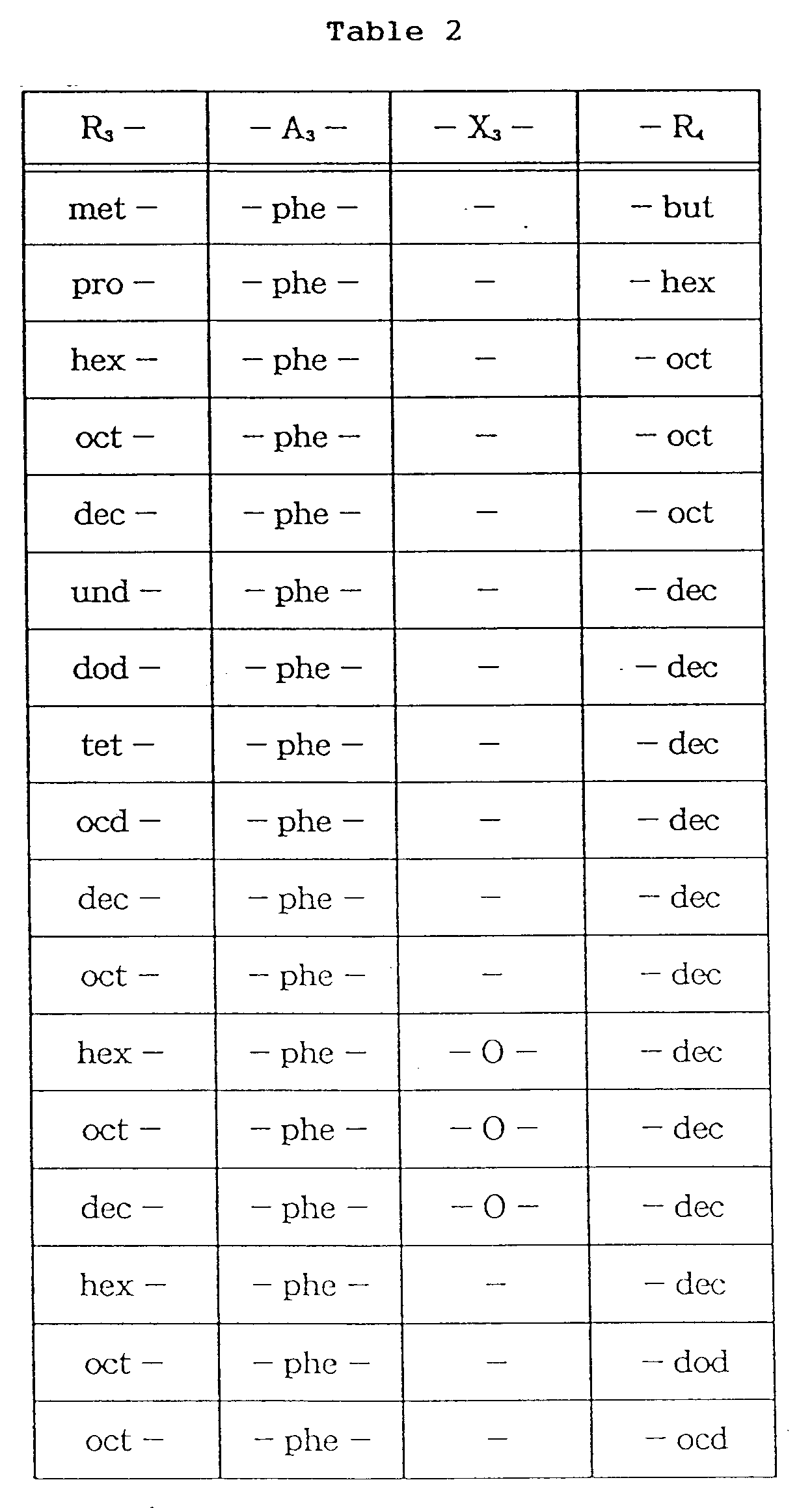

- In order to provide the liquid crystal composition according to the present invention with the third transition point in addition to the first and second transition point, it is preferred to incorporate a coumaran compound represented by the formula (C) in addition to the indan compound of the formula (A):

wherein R₅ and R₆ independently denote a linear or branched alkyl group having 1 - 18 carbon atoms; X₄ and X₅ independently denote a single bond, -O-, -CO·O- or -O·CO-; A₄ denotes a single bond,
- Preferred examples of the coumaran compound of the formula (C) may include those listed in the following Table 3, wherein the abbreviations represents the following side chain groups and ring groups:
met = CH₃, hep = C₇H₁₅, trt = C₁₃H₂₇, eth = C₂H₅,
oct = C₈H₁₇, tet = C₁₄H₂₉, pro = C₃H₇,
non = C₉H₁₉, ped = C₁₅H₃₁, but = C₄H₉,
dec = C₁₀H₂₁, hexd = C₁₆H₃₃, pen = C₅H₁₁,
und = C₁₁H₂₃, hepd = C₁₇H₃₅, hex = C₆H₁₃,
dod = C₁₂H₂₅, ocd = C₁₈H₃₇, 2mb = 2-methylbutyl,
phe =
pyr1 =
pry2 =
cyc =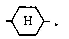


- The liquid crystal composition according to the present invention may preferably contain at least one species each of the indan compound of the formula (A), the quinoxaline compound of the formula (B) and/or the coumaran compound of the formula (C) in a proportion of 1 - 30 wt. %, preferably 5 - 30 wt. %, further preferably 8 - 25 wt. %, respectively.
- The liquid crystal composition according to the present invention may be formulated by incorporating as desired one or more species of other mesomorphic compounds, e.g., represented by the following formulae (D) - (H):

wherein n and m are independently 0, 1 or 2 satisfying

wherein A₆ denotes
X₆ denotes hydrogen or fluoride; R₉ and R₁₀ independently denote hydrogen, halogen CN or a linear, branched or cyclic alkyl group having 1 - 18 carbon atoms wherein one or more methylene groups can be replaced with -O-, -S-, -CO-, -CHW- (W = halogen, CN or CF₃), -CH=CH- or -C≡C- with the proviso that two hetero-atoms cannot be adjacent to each other, and R₉ and R₁₀ can be optically active.
wherein B₁ denotes
and R₁₁ and R₁₂ independently denote hydrogen, halogen, CN or a linear, branched or cyclic alkyl group having 1 - 18 carbon atoms wherein one or more methylene groups can be replaced with -O-, -S-, -CO-, -CHW- (W = halogen, CN or CF₃), -CH=CH- or -C≡C- with the proviso that two hetero-atoms cannot be adjacent to each other, and R₁₁ and R₁₂ can be optically active.
wherein C₁ denotes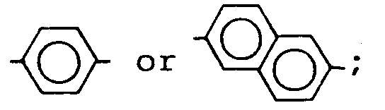
Z denotes -O- or -S-; R₁₃ and R₁₄ independently denote hydrogen, halogen, CN or a linear, branched or cyclic alkyl group having 1 - 18 carbon atoms wherein one or more methylene groups can be replaced with -O-, -S-, -CO-, -CHW- (W = halogen, CN or CF₃), -CH=CH- or -C≡C- with the proviso that two hetero-atoms cannot be adjacent to each other, and R₁₃ and R₁₄ can be optically active.
wherein R₁₅ and R₁₆ independently denote hydrogen, halogen, CN or a linear, branched or cyclic alkyl group having 1 - 18 carbon atoms wherein one or more methylene groups can be replaced with -O-, -S-, -CO-, -CHW- (W = halogen, CN or CF₃), -CH=CH- or -C≡C- with the proviso that two hetero-atoms cannot be adjacent to each other, and R₁₅ and R₁₆ can be optically active. - Preferred structural examples of the compounds of the formulae (D) - (G) may include those enumerated hereinbelow.
-

-

-
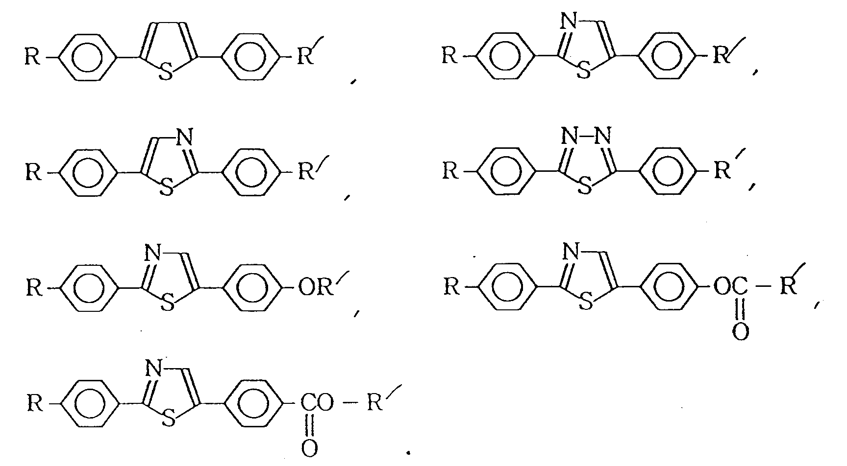
-

- In the above formulae, R and R' independently denote hydrogen, halogen, CN or a linear, branched or cyclic alkyl group having 1 - 18 carbon atoms wherein one or more methylene groups can be replaced with -O-, -S-, -CO-, -CHW- (W = halogen, CN or CF₃), -CH=CH- or -C≡C- with the proviso that two hetero-atoms cannot be adjacent to each other, and R and R' can be optically active; and X₆ denotes hydrogen or fluorine.
- It is preferred that the mesomorphic compounds represented by the formulae (D) - (H) constitute in total at least 30 wt. %, more preferably 50 - 90 wt. %, of the liquid crystal composition according to the present invention.
- Figure 4 is a schematic sectional view of an embodiment of the liquid crystal device using a chiral smectic liquid crystal layer for describing a structure of the liquid crystal device utilizing ferroelectricity.
- Referring to Figure 4, the liquid crystal device includes a chiral smectic
liquid crystal layer 1 disposed between a pair ofglass substrates 2 each having thereon atransparent electrode 3 and analignment control layer 4.Lead wires 6 are connected to theelectrodes 3 so as to apply a driving voltage to theliquid crystal layer 1 from apower supply 7. Outside thesubstrates 2, a pair ofpolarizers 8 are disposed so as to modulate incident light I₀ from alight source 9 in cooperation with theliquid crystal 1 to provide modulated light I. - Each of two
glass substrates 2 is coated with atransparent electrode 3 comprising a film of In₂O₃, SnO₂ or ITO (indium-tin-oxide) to form an electrode plate. Further thereon, analignment control layer 4 is formed by rubbing a film of a polymer such as polyimide with gauze or acetate fiber-planted cloth so as to align the liquid crystal molecules in the rubbing direction. Generally, it is possible to compose the alignment control layer from an insulating material including an inorganic material, such as silicon nitride, silicon nitride containing hydrogen, silicon carbide, silicon carbide containing hydrogen, silicon oxide, boron nitride, boron nitride containing hydrogen, cerium oxide, aluminum oxide, zirconium oxide, titanium oxide, or magnesium fluoride, and also an organic insulating material, such as polyvinyl alcohol, polyimide, polyamide-imide, polyester-imide, polyparaxylylene, polyester, polycarbonate, polyvinyl acetal, polyvinyl chloride, polyvinyl acetate, polyamide, polystyrene, cellulose resin, melamine resin, urea resin, acrylic resin, or photoresist resin. Such an alignment control layer can be composed of two layers. Alternatively, it is also possible to use a single layer of inorganic insulating alignment control layer or organic insulating alignment control layer. An inorganic alignment control layer may be formed by vapor deposition, while an organic alignment control layer may be formed by applying a solution of an organic insulating material or a precursor thereof in a concentration of 0.1 to 20 wt. %, preferably 0.2 - 10 wt. %, by spinner coating, dip coating, screen printing, spray coating or roller coating, followed by curing or hardening under prescribed hardening condition (e.g., by heating). The inorganic insulating layer may have a thickness of ordinarily 30 Å - 1 µm, preferably 40 - 3000 Å, further preferably 40 - 1000 Å. - The two
glass substrates 2 withtransparent electrodes 3 and further withalignment control layers 4 thereof are held to have a prescribed (but arbitrary) gap with aspacer 10 and a sealing member 5. For example, such a cell structure with a prescribed gap may be formed by sandwichingspacers 10 of silica beads or alumina beads having a prescribed diameter with two glass plates, and then sealing the periphery thereof with an sealing member 5 of, e.g., an epoxy adhesive. Alternatively, a polymer film or glass fiber may also be used as a spacer. Between the two glass plates, a chiral smectic liquid crystal is sealed up to provide a liquid crystal layer in a thickness of generally 0.5 to 20 µm, preferably 1 to 5 µm. - It is desired that the
liquid crystal 1 has an SmC* phase (chiral smectic C phase) in a broad temperature range including room temperature, particular at a lower temperature side thereof, and provides a device showing a broad drive voltage margin and a broad drive temperature margin. - Further, in order to show a monodomain state in a good alignment characteristic in a device, it is preferred that the liquid crystal has a phase transition series of isotropic - Ch (cholesteric) phase - SmA (smectic A) phase - SmC* (chiral smectic C) phase.
- The
transparent electrodes 3 are connected to theexternal power supply 7 through thelead wires 6. Further, outside theglass substrates 2,polarizers 8 are applied. Behind thepolarizer 8 is disposed optionally alight source 9. - The liquid crystal device according to the present invention may be provided with improved characteristics inclusive of a contrast by appropriately adjusting the device manufacturing conditions, such as a cell gap (liquid crystal layer thickness) between the substrates, and materials and rubbing conditions for the alignment control layer in combination with the liquid crystal composition according to the invention so as to satisfy the above-mentioned formulae (2), (3) and (4).
- In a specific example, an embodiment of liquid crystal device having a structure similar to that shown in Figure 4 was prepared in the following manner.
- Two 1.1 mm-thick glass plates as
substrates 2 were respectively provided withtransparent tripe electrodes 3 of ITO (indium tin oxide) together with side metal electrodes (not shown) of molybdenum and was further coated thereon with a 1500 Å-thick transparent dielectric film of tantalum oxide (not shown) by sputtering. - Onto the tantalum oxide film, an NMP solution of a polyimide precursor (e.g., "LQ-1802", mfd. by Hitachi Kasei K.K.; "LP-64" mfd. by Toray K.K., and "RN-305" mfd. by Nissan Kagaku K.K.) was applied by a printing method and baked at 200 - 270 oC to form a 100 to 300 Å-thick polyimide
alignment control film 4. After the baking, thefilm 4 was rubbed with an acetate fiber yarn-planted cloth. The pretilt angle may be controlled by appropriately selecting and combining the rubbing intensity governed by the rubbing cloth rotation speed and substrate feed speed and the polyimide alignment film materials. - Thus, the two substrates were treated in the above-described manner. Then, on one substrate, epoxy resin adhesive particles having an average particle size of 5.5 µm ("Toraypearl" mfd. by Toray K.K.) were dispersed at a density of 50 particles/mm² according to the Nordson electrostatic dispersion scheme. On the other substrate, silica microbeads having na average particle size of 1.2 µm was dispersed as
spacers 10 at a density of 300 particles/mm² by the Nordson electrostatic dispersion scheme. Then, onto one substrate, a liquid epoxy adhesive ("STRUCT BOND", mfd. by Mitsui Toatsu Kagaku K.K.) was applied by printing in a thickness of 6 µm. Then, the two substrates were applied to each other so that their rubbing directions were dispose in almost identical directions but with an anticlockwise intersection angle of 0 - 10 degrees and press-bonded to each other under a pressure of 2.8 kg/cm² for 5 min. at 70 oC, followed by heating at 150 oC under a pressure of 0.623 kg/cm² for 4 hours to cure the two types of adhesives, thereby preparing a blank cell. - Then, the cell was evacuated to a reduced pressure of 10⁻⁴ atm and filled with a ferroelectric liquid crystal composition heated to its isotropic phase to provide a liquid crystal cell.
- The liquid crystal cell thus prepared may be sandwiched between a pair of
polarizers 8 and driven by application of drive voltages from anexternal voltage supply 7 as illustrates in Figure 4. - A liquid crystal device according to the present invention may preferably be used to constitute a display apparatus in combination with a drive circuit and a light source.
- More specifically, a liquid crystal display apparatus may be constituted by using the liquid crystal device for a display panel and by adopting an arrangement and data format comprising image data accompanied with scanning line address data and also a communication synchronization scheme using a SYNC signal as shown in Figures 5 and 6.
- Image data are generated in a
graphic controller 52 in an apparatus body and transferred to the display panel 53 (illuminated with a backlight (not shown)) by signal transfer means shown in Figures 5 and 6. Thegraphic controller 52 principally comprises a CPU (or GCPU, central processing unit) 512 and a VRAM (video-RAM, image data storage memory) 514 and is in charge of management and communication of image data between ahost CPU 513 and the liquid crystal display apparatus (FLCD) 51. The control of image display according to the present invention is principally accomplished by thegraphic controller 52. - In an actual operation of a liquid crystal device using a chiral smectic liquid crystal as a display panel, an electric field is applied between a pair of substrates via scanning electrodes and data electrodes disposed on the substrates, respectively, in the form of a matrix. For example, Figure 7 is a waveform diagram showing a set of drive waveforms for effecting image display on the display panel wherein at SN and SN+1 are shown voltage waveforms applied to scanning electrodes SN and SN+1, and at I is shown a voltage waveform applied to a data electrode I, whereby voltages as shown at SN - I and SN+1 - I are applied to pixels at the intersections of the scanning electrodes and the data electrode.
- Hereinbelow, the present invention will be described more specifically based on Examples. In such Examples, liquid crystal compositions were evaluated by incorporating them in liquid crystal devices having a structure similar to that described with reference to Figure 4 and prepared in a process similar to the one described above.
- The parameters, such as response speed cone angle Ⓗ , apparent tilt angle ϑa, liquid crystal layer inclination angle δ, pretilt angle α, and smectic layer spacing d discussed herein, are based on values measured according to the following methods.
- A sample device sandwiched between right-angle cross-nicol polarizers was supplied with rectangular pulse waves of ±10.0 volts and 5.0 Hz, and a time required for causing a light quantity change of 0 to 90 % was measured as a response time τ representing a response speed while observing the optical response through a photomultiplier (available from Hamamatsu Photonics K.K.).
- A sample liquid crystal device was sandwiched between right angle-cross nicol polarizers and rotated horizontally relative to the polarizers under application of an AC voltage of ±30 V to ±50 V and 100 Hz between the upper and lower substrates of the device while measuring a transmittance through the device by a photomultiplier (available from Hamamatsu Photonics K.K.) to find a first extinct position (a position providing the lowest transmittance) and a second extinct position. A cone angle Ⓗ was measured as a half of the angle between the first and second extinct positions.
- A sample device sandwiched between right angle cross nicol polarizes was supplied with a single pulse of one polarity exceeding the threshold voltage of the ferroelectric liquid crystal and was then rotated under no electric field horizontally relative to the polarizers to find a first extinction position. Then, the device was supplied with a single pulse of the opposite polarity exceeding the threshold voltage of the liquid crystal and was then rotated under no electric field relative to the polarizers to find a second extinct position. An apparent tilt angle ϑa was measured as a half of the angle between the first and second extinct positions.
- The methods used were basically similar to the method used by Clark and Lagerwall (Japan Display '86, Sept. 30 - Oct. 2, 1986, p.p. 456 - 458) or the method of Ohuchi et al (J.J.A.P., 27 (5) (1988), p.p. 725 - 728). The measurement was performed by using a diffraction apparatus (available from MAC Science having a rotary cathode-type X-ray generating unit as shown in Figure 8), and 80 µm-thick glass sheets ("Microsheets", available from Corning Glass Works) were used as substrates so as to minimize the heat capacity and the X-ray absorption with the glass substrates.
- More specifically, for measurement of the layer spacing d, a system as shown in Figure 8 was used, wherein a sample
liquid crystal composition 801 was applied in a 5 mm-square size so as to form a flat surface on the 80 µm-thick glass sheet and, while being temperature-controlled by a temperature-controllingplate 805 and a temperature-monitoring thermocouple 806, irradiated with X rays from arotary X-ray source 802, so that the output light including diffraction rays was detected by a detector (counter) 803, similarly as in the ordinary powder X-ray diffraction. An angle providing a peak of X-ray intensity was substituted in the Bragg's formula for diffraction condition to obtain a layer spacing d. - Each sample liquid crystal composition was first brought to its isotropic phase temperature, and the measurement was repeated every 5 oC or every 1 oC in the vicinity of a transition point while cooling the sample down to a temperature where no diffraction peak was observed. The automatic temperature controller including the
plate 805 and themonitoring thermocouple 804 allowed a control accuracy of ±0.3 oC at each measurement temperature. - The measurement was performed by using CuKα-rays (1.54050 Å) at a power of 45 kV-100 mA as analyzing rays and using a slit system including DS of 0.05 mm, SS of 0.05 mm and RS of 0.05 mm. The scanning was performed at a rate of 3 deg./min.
- For the measurement of smectic layer inclination angle δ, a sample cell having a cell gap of 80 µm was prepared by using a pair of the 80 µm-thick glass sheets while using the same glass sheet as a spacer. A sample liquid crystal composition filling the sample cell was heated to isotropic phase and then gradually cooled to be homogeneously aligned under application of a magnetic field in a direction parallel to the substrates by an electromagnet. Then, the X-ray detector was set at the angle 2ϑ giving the above-mentioned layer spacing d, and the sample cell was subjected to ϑ-scanning. From the measured values, δ was calculated according to the method described in the above-mentioned references.
- According to the above-described method, it is possible to obtain a layer inclination angle δ intrinsic to a sample liquid crystal composition while substantially removing the effect of a cell thickness thereon. However, it is also possible to obtain a substantially identical δ value in the temperature range of ca. 20 oC to 60 oC by using a 1.2 µm-thick cell having rubbed alignment films of polyimides (like those obtained from "LP-64", "SP-710" or "SP-510" described above) instead of such an 80 µm-thick cell subjected to a magnetic field aligning treatment.
- The measurement was performed according to the crystal rotation method as described at Jpn. J. Appl. Phys. vol. 19 (1980), No. 10, Short Notes 2013.
- More specifically, a pair of substrates rubbed in mutually parallel and opposite directions were applied to each other to form a cell having a cell gap of 20 µm, which was then filled with a liquid crystal mixture assuming SmA phase in the temperature range of 10 - 55 oC obtained by mixing 80 wt. % of a ferroelectric liquid crystal ("CS-1014", mfd. by Chisso K.K.) with 20 wt. % of a compound represented by the following formula:

- For measurement, the liquid crystal cell was rotated in a plane perpendicular to the pair of substrates and including the aligning treatment axis and, during the rotation, the cell was illuminated with a helium-neon laser beam having a polarization plane forming an angle of 45 degrees with respect to the rotation plane in a direction normal to the rotation plane, whereby the intensity of the transmitted light was measured by a photodiode from the opposite side through a polarizer having a transmission axis parallel to the polarization plane.
- Then, the transmitted light intensity spectrum obtained by interference was fitted by simulation to the following theoretical formulae (12) and (13), thereby obtaining a pretilt angle α.


In the above formula, the symbols represent the following parameters: - No:
- refractive index of ordinary ray,
- Ne:
- refractive index of extraordinary ray,
- φ:
- rotation angle of the sample cell,
- T(φ):
- transmitted light intensity,
- d:
- cell thickness,
- λ:
- wavelength of incident light
- A sample liquid crystal device disposed between right-angle cross-nicol polarizers was supplied with a single pulse of one polarity to uniformly form one stable state and then rotated relative to the polarizers to find a first extinction position. The liquid crystal device fixed at the position was then supplied with a single pulse of the opposite polarity to form another stable state giving a bright state at the observed position. The output voltage from a photomultiplier in this state is divided by the output voltage in the extinction position to provide a contrast.
- Electrodes on a pair of substrates of a sample liquid crystal device disposed between a pair of right-angle cross-nicol polarizers were supplied with a combination of a scanning signal, e.g., as shown at SN and a data signal, e.g., as shown at I in Figure 7 so as to write a dark state and a bright state, respectively while varying a pulse duration T at a fixed peak value Vop allowable ranges of T for stably providing a dark state and a bright state were measured. In case where the ranges for T are determined as shown in Figure 8, for example, a drive margin M is given by the following formula (14):

wherein T₁ is a minimum width for stably writing a bright state and T₂ is a maximum width for stably writing a dark state. The drive margin M has a larger value if a larger overlapping of the ranges T₁ and T₂ for writing dark and bright states is obtained. - The phase transition temperatures of each liquid crystal composition were measured by a DSC (differential scanning calorimeter) in combination with an observation of a cell containing the liquid crystal composition through a polarizing microscope.
- Table 4 below shows phase transition temperatures (oC, on temperature decrease), SmA phase temperature range width (oC) and types of temperature-dependent layer spacing d-changing characteristic for liquid crystal compositions A - K and other commercially available compositions ("CS-1017", available from Chisso K.K.; and "ZLI-3233" available from Merck Co.) used in Examples 1 - 20 appearing hereinafter. The temperature-dependent layer spacing-changing characteristics are also shown in Figures 10 - 12.
- The temperature-dependent layer spacing d-changing characteristics shown in Table 4 are characterized by types I - V according to the following standards:
- I: In SmC* phase, the layer spacing d decreases and then increases on temperature decrease, thus having a minimum value dmin.
- II: In SmC* phase, the layer spacing d decreases on temperature decrease and has no minimum value dmin.
- III: In SmA phase, the layer spacing d increases on temperature decrease.
- IV: In SmA phase, the layer spacing d is constant.
- V: In SmA phase, the layer spacing d decreases on temperature decrease.
- The liquid crystal compositions A - H shown in Table 4 are all compositions comprising a phenylpyrimidine-type mesomorphic compound as a principal component.
- The liquid crystal compositions I, J and K include the component compounds identified by their structural formulae shown below in the respectively indicated proportions:
-


-


-


- The temperature-dependence of response speed (response time) was evaluated with respects to liquid crystal compositions showing a minimum (second transition point) of layer spacing and liquid crystal compositions having no minimum. The results are shown in Table 5 below.
- Each device was prepared by using "LQ-1802" for alignment control films so as to provide a pretilt angle of ca. 17 deg., a rubbing intersection angle of 8 deg., and a cell gap of 1.2 µm.

- From the above results, the liquid crystal compositions CS-1017 and ZLI-3233 having no minimum (second transition point) of layer spacing in SmC* phase showed temperature characteristic factor f10/50 regarding response speed (a ratio of response time between 10 oC and 50 oC) which were 15 or larger in an expected environmental temperature range of 10 - 50 oC for a liquid crystal display device. On the other hand, the liquid crystal compositions A, D and F having a minimum (second transition point) of layer spacing in SmC* phase showed temperature characteristic factors f10/50 on the order of 3 - 4 indicating an improved temperature-dependence of response speed.
- Some liquid crystal compositions all having a minimum (second transition point) of liquid crystal in SmC* phase including some compositions (A, C, D and F) of which the layer spacing increased or was constant on temperature decrease in SmA phase and other compositions (B and E) of which the layer spacing decreased on temperature decrease in SmA phase, were examined with respect to a contrast change before and after a temperature increase spanning the phase transition temperature of SmC* phase to SmA phase. The results are shown in Table 6.
- More specifically, each liquid crystal device was prepared by using "LQ-1802" for alignment control films so as to provide a pretilt angle of ca. 19 degrees, a rubbing intersection angle of 6 degrees, and a cell gap of 1.1 µm.
- Each liquid crystal device prepared was heated from room temperature at a rate of 1 oC/min. up to a temperature which was 5 oC above the SmC* → SmA transition temperature and retained for 10 hours at that temperature, followed by cooling to room temperature at a rate of 1 oC/min. The contrast of each device was measured at 30 oC respectively before and after the heating.

- From the above results, it is understood that the liquid crystal compositions A, C, D and F having a minimum (second transition point) of layer spacing in SmC* and also a layer spacing increasing or being constant in SmA phase, showed much less contrast change before and after heating over the SmC* → SmA phase transition temperature, compared with the liquid crystal compositions B and E having a layer spacing which decreased on temperature decrease in SmA phase. Thus, such compositions A, C, D and F caused little change in alignment state even under heating over the phase transition temperature and were estimated to show stable characteristics, particularly stable display characteristics, even after a storage at higher temperatures.
- Among liquid crystal compositions having a minimum dmin (second transition point) of layer spacing in SmC* phase, compositions satisfying and not satisfying the following formula (8) between dmin and dA (layer spacing at a first transition point in the vicinity of the SmA → SmC* phase transition temperature) were evaluated with respect to drive margin:

The results are shown in Table 7. - Each device was prepared by using "LQ-1802" for alignment control films so as to provide a pretilt angle of ca. 16 degrees, a rubbing intersection angle of 8 degrees, and a cell gap of 1.2 µm. The drive margin was measured while setting the writing peak voltage Vop at 15 volts (in the waveform shown in Figure 7).

- From the above results, among the liquid crystal compositions having a minimum dmin of layer spacing in SmC* phase, those compositions A, D and F satisfying the formula (8) provided a sufficient drive margin over an expected operational environmental temperature range of 10 - 50 oC for a liquid crystal display device, but the compositions C, G and H not satisfying the formula (8) resulted in a drive margin over a narrower temperature range and the resultant drive margin values were rather small.
- The temperature-dependence of response speed was evaluated with respect to liquid crystal compositions containing an indan compound or/and quinoxaline compound. The results are shown in Tables 8-1 and 8-2 below.
- Each device was prepared by using "LQ-1802" for alignment control films so as to provide a pretilt angle of ca. 18 degrees, a rubbing intersection angle of 8 degrees, and a cell gap of 1.2 µm.

- Compared with the compositions of Examples 4 and 5 shown in Table 1, the composition I of Example 18 showing Type I of temperature-dependent layer spacing-changing characteristic in SmC* phase, showed a much smaller temperature-dependence of response speed.
- Further, the composition J and K containing both indan compound and quinoxaline compound also showed Type I of temperature-dependence layer spacing-changing characteristic and further smaller temperature-dependence of response speed. This tendency was also confirmed with respect to other compositions containing both indan compound and quinoxaline compound, which were thus regarded to be suitable as liquid crystal compositions showing the characteristics required by the present invention.
- Table 9 below shows phase transition temperatures (generally, on temperature decrease) and Table 10 below shows types of temperature-dependent layer spacing d-changing characteristics in smectic phase and characteristic ratios dmin/dA, dmax/dA and dc/dA (wherein dA: layer spacing at the first transition point, dmax: layer spacing at the third transition point; dmin: layer spacing at the second transition point; and dc: a minimum value of layer spacing below the third transition point in SmC* phase down to another lower-temperature), respectively, of liquid crystal compositions L - V and commercially available composition "CS-1017" and "ZLI-3233". The temperature-dependent layer spacing d-characteristics are also shown in Figures 13 - 16.
- None of the liquid crystal compositions L - V caused crystallization even at -25 oC when they were contained in a liquid crystal device.
- The temperature-dependent layer spacing d-changing characteristics shown in Table 10 are characterize by types VI - IX according to the following standards:
- VI: The layer spacing d in smectic phase almost monotonously decreases on temperature decrease regardless of whether or not it shows a first transition point where the layer spacing d abruptly decreases (in other words, an ordinary temperature-dependent layer spacing-changing characteristic).
- VII: The layer spacing d assumes a first transition point in the neighborhood of SmA → SmC* phase transition temperature on temperature decrease and further assumes a minimum dmin at a second transition point at which the layer spacing d turns to increase on further temperature decrease.
- VIII: On temperature decrease, the layer spacing d assumes the first and second transition points, and also a third transition point where the layer spacing d turns to decrease on further temperature decrease, and further satisfies the following formula (10) between dc and dA:

- IX: The layer spacing-changing characteristic satisfies the above conditions VIII and also satisfies the following formula (11):

- The liquid crystal compositions L, N, P, Q, R and S in Tables 9 and 10 are all compositions comprising a phenylpyrimidine-type mesomorphic compound as a principal component.
- The liquid crystal compositions M, O, T, U and V have the following compositions.
-

-


-


-
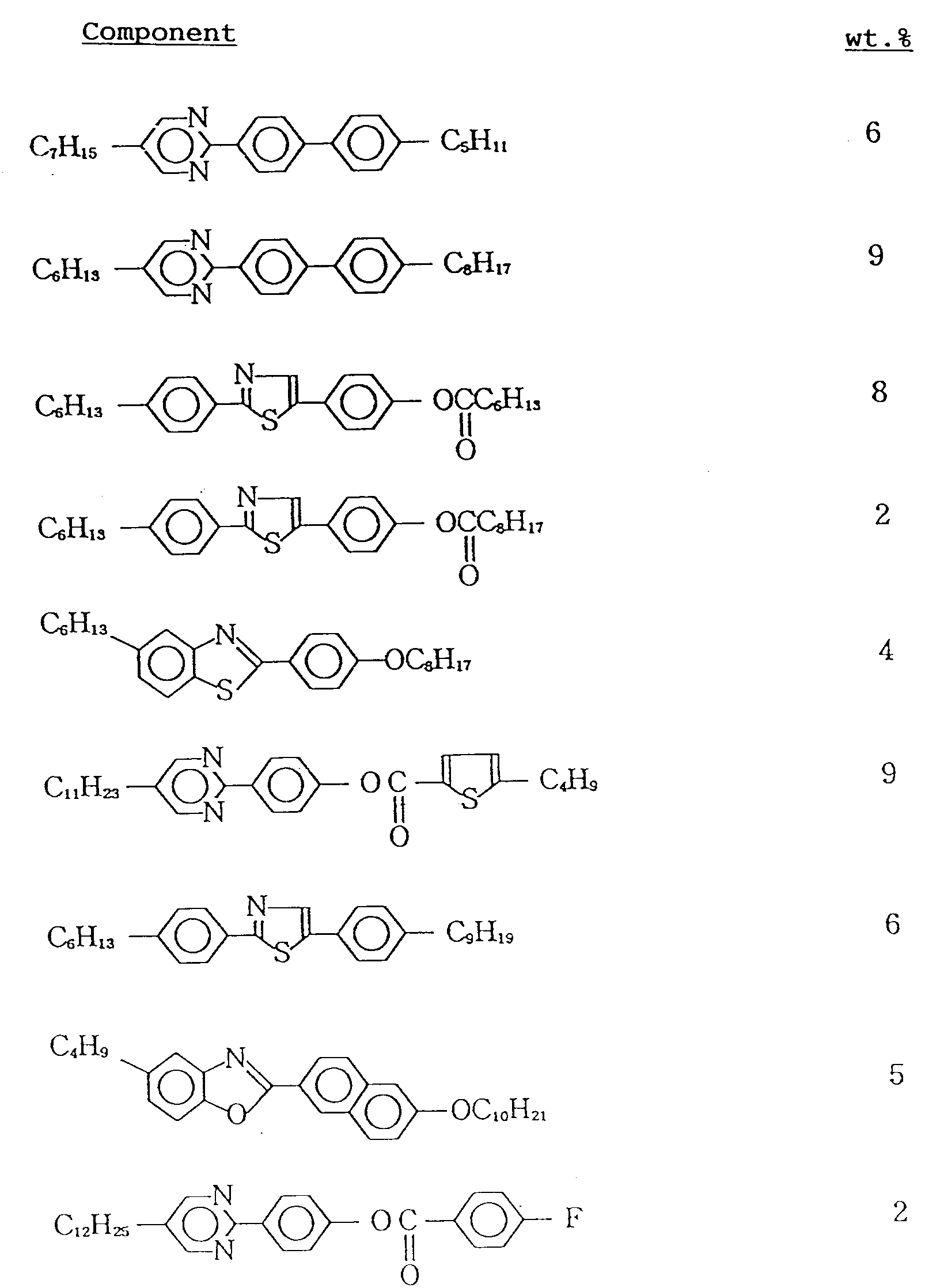

-


- The temperature-dependence of response speed (response time) was evaluated with respect to commercially available liquid crystal compositions "CS-1017" (available from Chisso K.K.) and "ZLI-3233" (available from Merck Co.) showing Type VI layer spacing-changing characteristic and liquid crystal compositions L - R showing Type VII - IX layer spacing-changing characteristic.
- Each liquid crystal device was prepared to have a structure similar to the one described with reference to Figure 4 similarly as those used in Examples 1 - 20. More specifically, each device was prepared in the following manner.
- Two 0.7 mm-thick glass sheets as substrates were coated with ITO films and further with insulating films. Each substrate was further coated with a polyimide resin precursor, followed by baking and rubbing with an acetate fiber yarn-planted cloth. Then, two substrates were applied to each other so as to form a cell gap of ca. 1.5 µm, which was then filled with a sample liquid crystal composition in isotropic phase or cholesteric phase, followed by gradual cooling to room temperature to provide a liquid crystal device.
- Each liquid crystal device was subjected to measurement of response speed (response time) and the temperature dependence thereof was evaluated in terms of a temperature characteristic factor f10/40 (a ratio of response time between 10 oC and 40 oC). A smaller value of f10/40 represents a better temperature dependence of response speed.
- The results are shown in Table 11 below.

- The results in Table 11 above show that the liquid crystal compositions showing Types VII - IX of layer spacing-changing characteristic (i.e., the layer spacing d assumes a first transition point in the vicinity of the SmA → SmC* phase transition temperature on temperature decrease and, on further temperature decrease, assumes a minimum (second transition point)) showed an improved temperature-dependence of response speed compared with the liquid crystal compositions showing Type VI of layer spacing changing characteristic (i.e., on temperature decrease, the layer spacing d in smectic phase monotonously decreases after having a first transition point or showing no flexural point in the neighborhood of the SmA → SmC* phase transition temperature).
- The changes in alignment state and response speed characteristic due to low-temperature storage were examined.
- Each sample device having a structure similar to the one described with reference to Figure 4 was prepared in the following manner.
- Two 1.1 mm-thick glass plates as substrates were respectively provided with transparent tripe electrodes of ITO (indium tin oxide) together with side metal electrodes of molybdenum and was further coated thereon with a 1500 Å-thick transparent dielectric film of tantalum oxide (not shown) by sputtering.
- Onto the tantalum oxide film, an NMP solution of a polyimide precursor ("LQ-1802", mfd. by Hitachi Kasei K.K.) was applied by a printing method and baked at 270 oC to form a 300 Å-thick polyimide alignment control film. After the baking, the film was rubbed with an acetate fiber yarn-planted cloth.
- Thus, the two substrates were treated in the above-described manner. Then, on one substrate, epoxy resin adhesive particles having an average particle size of 5.5 µm ("Toraypearl" mfd. by Toray K.K.) were dispersed at a density of 50 particles/mm² according to the Nordson electrostatic dispersion scheme. On the other substrate, silica microbeads having an average particle size of 1.5 µm were dispersed at a density of 300 particles/mm² by the Nordson electrostatic dispersion scheme. Then, onto one substrate, a liquid epoxy adhesive ("STRUCT BOND", mfd. by Mitsui Toatsu Kagaku K.K.) was applied by printing in a thickness of 6 µm. Then, the two substrates were applied to each other so that their rubbing directions were dispose in almost identical directions but with an anticlockwise intersection angle of 8 degrees and press-bonded to each other under a pressure of 2.8 kg/cm² for 5 min. at 70 oC, followed by heating at 150 oC under a pressure of 0.63 kg/cm² for 4 hours to cure the two types of adhesives, thereby preparing a blank cell.
- Then, the cell was evacuated to a reduced pressure of 10 Pa and filled with a sample liquid crystal composition heated to its isotropic phase to provide a liquid crystal device (panel).
- Each liquid crystal device (panel) had a picture area defined by a lateral size of ca. 280 mm (data line side) and a vertical size of ca. 220 mm (scanning line side) providing 1280 x 1024 pixels.
- For the low-temperature storage test, the respective sample liquid crystal panels were placed in a large-sized thermostatic vessel and cooled from room temperature at a rate of 1 oC/min. to -25 oC while controlling the temperature so as to provide a substantially uniform temperature over the entire panel face, followed by standing for 5 hours at -25 oC and temperature-raising to room temperature at a rate of 3 oC/min. Then, the alignment state and response speed of each sample panel were measured and compared with those before the low-temperature storage.
- The results are shown in the following Table 12.
Table 12 Example Composition Type of d change Change after storage for 5 hours at -25oC 28 O VIII no change 29 P VIII no change 30 Q IX no change 31 L VII ϑa*¹ and speed*² 32 M VII ϑa*¹ and speed*² 33 N VII ϑa*¹ and speed*² Note
*1) ϑa: The apparent tilt angle ϑa decreased after the low-temperature storage.*2) Speed: The response speed changed after the low temperature storage. - As is understood from the results shown in Table 12.
- The liquid crystal compositions L, M and N having Type VII of layer spacing-changing characteristic showed worse display performances, such as a decrease in ϑa resulting in a lower contrast and a change in response speed, after the low-temperature storage.
- On the other hand, the liquid crystal compositions O, P and Q having Type VIII or IX of layer spacing-changing characteristic showed substantially no change after 5 hours of low-temperature storage. Accordingly, it is suggested that a liquid crystal composition having a third transition point shows a stable performance even after low temperature storage.
- The changes in response speed and alignment state were examined by changing the conditions for the low-temperature storage. Liquid crystal compositions used were those having Type VII, VIII or IX of layer spacing-changing characteristic. Each sample panel was placed in a thermostatic vessel and cooled from room temperature at a rate of 1 oC/min. to -10 oC or -25 oC while effecting a temperature control so as to provide a uniform temperature over the entire panel face, followed by standing at -10 oC or -25 oC for 120 hours and temperature raising to room temperature at a rate of 3 oC/min or 3 oC/hour. Then, the alignment state and response speed of each sample panel were measured and compared with those before the low-temperature storage.
- The results are shown in the following Table 13 while representing the change after the low-temperature storage by a change in ϑa which was most noticeably caused.

- As is shown in Table 13, the liquid crystal compositions Q, R and S having Type IX of layer spacing-changing characteristic showed no change in alignment state even after low-temperature storage under any conditions. Further, among the liquid crystal compositions N and O having Type VIII of layer spacing-changing characteristic, the composition N showed no change in alignment state or response speed after a storage at -10 oC where d did not exceed dA.
- The liquid crystal compositions having Type VIII of layer spacing-changing characteristic caused a decrease in ϑa after a storage at a temperature (-25 oC) causing d to exceed dA in some cases but the composition O was substantially free from a change in display characteristic after storage at -25 oC in case where the panel was warmed at a higher rate of 3 oC/min. In this way, the effect of low-temperature storage could be different depending on a complex combination of factors, such as storage temperature, time and temperature-changing rate and could not be simply determined based on the storage temperature alone.
- In addition to the experiments of which the results are described above, a large number of liquid crystal compositions were tested regarding the temperature-dependence of response speed and change in alignment state due to a low-temperature storage. As a result, it has been found that a liquid crystal composition having a dc/dA ratio of at most 1.003 can withstand a low-temperature storage for a short period of ca. 5 hours. Further, a liquid crystal composition having a dmax/dA ratio of at most 1.003 can obviate occurrence of abnormalities due to low-temperature storage. On the other hand, a liquid crystal composition having a dmax/dA ratio smaller than 0.993 is liable to cause a slower response speed at low temperatures, thus making it difficult to effect a uniform image over a large-area panel over a wide temperature range.
- Accordingly, in view of a possibility that a product in the form of a liquid crystal apparatus can be stored at a very low temperature during transportation by air or storage in a warehouse and the temperature and storage time can be unknown, it is prefer to use a liquid crystal composition having Type IX of layer spacing-changing characteristic, i.e., satisfying the relationship of the formula (11).
- Experimental results are given showing that the inclusion of both an indan compound and a coumaran compound is effective in providing a liquid crystal compound having better low-temperature storability.
- The liquid crystal composition M contains none of indan compound or coumaran compound. On the other hand, the liquid crystal composition T contains 17 % of an indan compound; the composition U contains 17 % of an indan compound and 6 % of a coumaran compound; and the composition V contains 17 % of an indan compound and totally 5 % of two coumaran compounds. As a result, the compositions M, T, U and V showed Types VII, VIII, IX and IX, respectively, of layer spacing-changing characteristic, thus suggesting that the inclusion of both indan and coumaran compounds provided compositions (U and V) which were expected to show excellent low-temperature storage durability (Type IX of layer spacing-changing characteristic).
- A low-temperature storage test was performed by using these composition in the same manner as in Examples 34 - 39. The results are shown in the following Table 14.

- The expectation was confirmed by the experimental results. Thus, the composition U and V having Type IX of layer spacing-changing characteristic by inclusion of both indan and coumaran compounds caused no charge in display characteristics after the low temperature storage.
- As has been described in detail, the liquid crystal composition according to the present invention has been provided with improved temperature-dependence of performances including a response speed and sufficient drive margin over an expected operational temperature range in a liquid crystal device, particularly a display device. Further, if the layer spacing d changing characteristic in SmA phase is adjusted, the composition is provided with a suppressed change in drive characteristic at high temperatures and provides a high contrast even after a storage at high temperatures. Further, if the layer spacing d-changing characteristic in SmC* phase is further adjusted, the composition is provided with further improved low-temperature performances and provides a very stable alignment state even after storage at low temperatures. Accordingly, by using the liquid crystal composition and the liquid crystal device including the composition according to the present invention, it is possible to provide a liquid crystal apparatus, particularly a liquid crystal display apparatus, capable of exhibiting excellent display performances.
- A liquid crystal device with little temperature-dependence of drive characteristics, such as response speed, and with good storage stability, can be produced by using a liquid crystal composition, successively assuming SmA (smectic A) phase and SmC* (chiral smectic) phase on temperature decrease. The layer spacing composition has a temperature-dependence of layer spacing d in smectic phase such that the layer spacing d increases, is constant or decreases on temperature decrease in SmA phase temperature range, assumes a first transition point where the layer spacing d abruptly decreases on temperature decrease in vicinity of transition temperature from SmA phase to SmC* phase, and assumes a second transition point where the layer spacing d commences to increase on further temperature decrease below the first transition point in SmC* temperature range.


| Composition | Type of d change | dc/dA | dmax/dA | dmin/dA |
| CS-1017 | VI | - | - | - |
| ZLI-3233 | VI | - | - | - |
| L | VII | - | - | 0.994 |
| M | VII | - | - | 0.989 |
| N | VII | - | - | 0.991 |
| O | VIII | 1.000 | 1.006 | 0.983 |
| P | VIII | 1.003 | 1.006 | 0.985 |
| Q | IX | 0.998 | 1.000 | 0.986 |
| R | IX | 0.996 | 0.999 | 0.986 |
| S | IX | 0.988 | 0.996 | 0.982 |
| T | VIII | 1.000 | 1.004 | 0.986 |
| U | IX | 0.997 | 0.999 | 0.986 |
| V | IX | 0.996 | 0.998 | 0.985 |
Claims (30)
- A liquid crystal composition, successively assuming SmA (smectic A) phase and SmC* (chiral smectic) phase and SmC* (chiral smectic) phase on temperature decrease, said liquid crystal composition having a temperature-dependence of layer spacing d in smectic phase such that the layer spacing d increases, is constant or decreases on temperature decrease in SmA phase temperature range, assumes a first transition point where the layer spacing d abruptly decreases on temperature decrease in vicinity of transition temperature from SmA phase to SmC* phase, and assumes a second transition point where the layer spacing d commences to increase on further temperature decrease below the first transition point in SmC* temperature range.
- A liquid crystal composition according to Claim 1, causing a phase transition in successive order of isotropic (Iso) phase, cholesteric (Ch) phase, smectic A (SmA) phase and chiral smectic (SmC*) phase on temperature decrease.
- A liquid crystal composition according to Claim 1, assuming SmA phase over a temperature range of at least 20 oC.
- A liquid crystal composition according to Claim 1, wherein the layer spacing d assumes a value dA at the first transition point and a value dmin at the second transition point satisfying a relationship of

- A liquid crystal composition according to Claim 1, wherein the second transition point in SmC* phase is in the range of 20 - 50 oC.
- A liquid crystal composition according to Claim 1, having a cone angle Ⓗ which increases, assumes a certain maximum and then decreases on successive temperature decrease in SmC* phase.
- A liquid crystal composition according to Claim 1, containing at least one species of mesomorphic compound represented by the following formula (A):
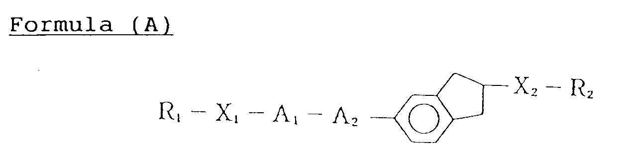

- A liquid crystal composition according to Claim 1, wherein the layer spacing d increases on temperature decrease or is constant in SmA phase temperature range.
- A liquid crystal composition according to Claim 8, wherein the layer spacing d assumes dA at said first transition point and dmin at said second transition point, satisfying a formula:

- A liquid crystal composition according to Claim 8, containing at least one species of mesomorphic compound represented by formula (A) below and at least one species of mesomorphic compound represented by formula (B) below:


- A liquid crystal composition according to Claim 10, wherein said mesomorphic compound represented by the formula (A) and said mesomorphic compound represented by the formula (B) are respectively contained in an amount of 1 - 30 wt. %.
- A liquid crystal composition according to Claim 1, wherein the layer spacing d assumes a third transition point where the layer spacing d turns to decrease on further temperature below the second transition point in SmC* phase.
- A liquid crystal composition according to Claim 12, wherein said second transition point is in the temperature range of 20 - 50 oC.
- A liquid crystal composition according to Claim 12, wherein said second transition point is in the temperature range of 30 - 50 oC.
- A liquid crystal composition according to Claim 12, wherein the layer spacing d assumes a value dA at the first transition point and a value dmin at the second transition point satisfying a relationship of

- A liquid crystal composition according to Claim 12, wherein the layer spacing d assumes a value dA at the first transition point and a value dmin at the second transition point satisfying a relationship of

- A liquid crystal composition according to Claim 12, wherein the layer spacing d assumes a minimum dc in a range below said transition point and within SmC* phase down to a lower temperature phase, satisfying a relationship with a layer spacing dA at the first transition point as follows:

- A liquid crystal composition according to Claim 17, wherein the layer spacing d assumes a value dA at the first transition point and a value dmin at the second transition point satisfying a relationship of

- A liquid crystal composition according to Claim 17, wherein the layer spacing d assumes a value dA at the first transition point and a value dmin at the second transition point satisfying a relationship of

- A liquid crystal composition according to Claim 12, wherein the layer spacing d assumes a value dA at the first transition point and a value dmax at the third transition point satisfying a relationship of

- A liquid crystal composition according to Claim 20, wherein the layer spacing d assumes a value dA at the first transition point and a value dmin at the second transition point satisfying a relationship of

- A liquid crystal composition according to Claim 20, wherein the layer spacing d assumes a value dA at the first transition point and a value dmin at the second transition point satisfying a relationship of

- A liquid crystal composition according to Claim 12, containing at least one species of mesomorphic compound represented by formula (A) below and at least one species of mesomorphic compound represented by formula (C) below:


- A liquid crystal composition according to Claim 23, wherein said mesomorphic compound represented by the formula (A) and said mesomorphic compound represented by the formula (C) are respectively contained in an amount of 1 - 30 wt. %.
- A liquid crystal device, comprising: a pair of substrates, and a liquid crystal composition according to any one of Claims 1 - 24 disposed between the substrates.
- A liquid crystal device according to Claim 25, wherein at least one of the substrates has thereon an alignment control layer.
- A liquid crystal device according to Claim 26, wherein said alignment control layer has been subjected to a uniaxial aligning treatment.
- A liquid crystal device according to Claim 25, wherein said pair of substrates are disposed with a gap therebetween which is small enough to release a helical structure of liquid crystal molecules of said liquid crystal composition disposed therebetween.
- A liquid crystal device according to Claim 25, wherein said pair of substrates are provided with alignment control layers having uniaxial alignment axes which intersect each other at a prescribed angle; and said liquid crystal composition is placed in an alignment state providing a pretilt angle α, cone angle H , and a smectic layer inclination angle δ in SmC* phase satisfying following formulae (2) and (3); and the liquid crystal composition in the alignment state assumes at least two stable states providing optical axes forming an angle 2ϑa therebetween (ϑa: apparent tilt angle) satisfying the following formula (4) with respect the cone angle H :


- A liquid crystal apparatus, comprising a liquid crystal device according to Claim 25, and means for driving the liquid crystal device.
Applications Claiming Priority (12)
| Application Number | Priority Date | Filing Date | Title |
|---|---|---|---|
| JP265621/93 | 1993-09-29 | ||
| JP265622/93 | 1993-09-29 | ||
| JP26562293 | 1993-09-29 | ||
| JP26562293 | 1993-09-29 | ||
| JP26562193 | 1993-09-29 | ||
| JP26562193 | 1993-09-29 | ||
| JP54526/94 | 1994-02-28 | ||
| JP54527/94 | 1994-02-28 | ||
| JP5452694 | 1994-02-28 | ||
| JP5452694 | 1994-02-28 | ||
| JP5452794 | 1994-02-28 | ||
| JP5452794 | 1994-02-28 |
Publications (2)
| Publication Number | Publication Date |
|---|---|
| EP0647695A1 true EP0647695A1 (en) | 1995-04-12 |
| EP0647695B1 EP0647695B1 (en) | 1999-12-15 |
Family
ID=27463077
Family Applications (1)
| Application Number | Title | Priority Date | Filing Date |
|---|---|---|---|
| EP94115262A Expired - Lifetime EP0647695B1 (en) | 1993-09-29 | 1994-09-28 | Liquid crystal composition, liquid crystal device and liquid crystal apparatus using same |
Country Status (3)
| Country | Link |
|---|---|
| US (1) | US5582763A (en) |
| EP (1) | EP0647695B1 (en) |
| DE (1) | DE69422126T2 (en) |
Cited By (9)
| Publication number | Priority date | Publication date | Assignee | Title |
|---|---|---|---|---|
| EP0768360A1 (en) * | 1995-10-12 | 1997-04-16 | Canon Kabushiki Kaisha | Liquid crystal composition, liquid crystal device, and liquid crystal display apparatus using same |
| EP0821048A3 (en) * | 1996-07-22 | 1998-10-28 | Canon Kabushiki Kaisha | Liquid crystal device |
| EP0962804A4 (en) * | 1997-10-01 | 2003-07-30 | Citizen Watch Co Ltd | Anti-ferroelectric liquid crystal display |
| WO2004048500A1 (en) * | 2002-11-22 | 2004-06-10 | Merck Patent Gmbh | Liquid crystal medium |
| CN102703093A (en) * | 2012-06-13 | 2012-10-03 | 江苏和成新材料有限公司 | Liquid crystal composition and liquid crystal display device comprising liquid crystal composition |
| CN102994100A (en) * | 2012-10-11 | 2013-03-27 | 江苏和成显示科技股份有限公司 | Liquid crystal composition and liquid crystal display device containing liquid crystal composition |
| CN103087724A (en) * | 2013-01-08 | 2013-05-08 | 江苏和成显示科技股份有限公司 | Liquid crystal composition and liquid crystal display device comprising same |
| CN105647542A (en) * | 2016-02-01 | 2016-06-08 | 北京华科嘉泰科技有限公司 | Liquid crystal compound containing 1,5-indan structure and preparation method and application thereof |
| CN107828426A (en) * | 2013-05-13 | 2018-03-23 | 达兴材料股份有限公司 | Liquid crystal medium and liquid crystal display device |
Families Citing this family (3)
| Publication number | Priority date | Publication date | Assignee | Title |
|---|---|---|---|---|
| US5932136A (en) * | 1995-10-20 | 1999-08-03 | Canon Kabushiki Kaisha | Liquid crystal device and liquid crystal apparatus |
| JPH11100577A (en) * | 1997-07-31 | 1999-04-13 | Canon Inc | Liquid crystal alignment method, liquid crystal element manufacturing method, liquid crystal element obtained by the manufacturing method, liquid crystal device |
| US7216002B1 (en) * | 2001-10-22 | 2007-05-08 | Gateway Inc. | System and method for group content selection |
Citations (3)
| Publication number | Priority date | Publication date | Assignee | Title |
|---|---|---|---|---|
| EP0546338A1 (en) * | 1991-11-12 | 1993-06-16 | Canon Kabushiki Kaisha | Mesomorphic compound, liquid crystal composition, liquid crystal device, display apparatus and display method |
| EP0548548A1 (en) * | 1991-11-22 | 1993-06-30 | Canon Kabushiki Kaisha | Liquid crystal composition, liquid crystal device and display apparatus |
| EP0571955A1 (en) * | 1992-05-26 | 1993-12-01 | Canon Kabushiki Kaisha | Liquid crystal composition and liquid crystal device using the same |
Family Cites Families (7)
| Publication number | Priority date | Publication date | Assignee | Title |
|---|---|---|---|---|
| US4367924A (en) * | 1980-01-08 | 1983-01-11 | Clark Noel A | Chiral smectic C or H liquid crystal electro-optical device |
| JPS6031120A (en) * | 1983-07-30 | 1985-02-16 | Canon Inc | Driving method of optical modulating element |
| JP2774502B2 (en) * | 1987-11-26 | 1998-07-09 | キヤノン株式会社 | Display device, drive control device thereof, and display method |
| JP2612503B2 (en) * | 1990-03-02 | 1997-05-21 | キヤノン株式会社 | Liquid crystal element |
| JP2941972B2 (en) * | 1991-02-14 | 1999-08-30 | キヤノン株式会社 | Liquid crystal composition, liquid crystal element having the same, display method and display device using the same |
| JP3039735B2 (en) * | 1991-11-12 | 2000-05-08 | キヤノン株式会社 | Liquid crystal compound, liquid crystal composition containing the same, liquid crystal element having the same, display method and display device using the same |
| JP3308626B2 (en) * | 1992-02-12 | 2002-07-29 | キヤノン株式会社 | Liquid crystal compound, liquid crystal composition containing the same, liquid crystal element having the same, display method using them, and display device |
-
1994
- 1994-09-28 US US08/314,422 patent/US5582763A/en not_active Expired - Lifetime
- 1994-09-28 EP EP94115262A patent/EP0647695B1/en not_active Expired - Lifetime
- 1994-09-28 DE DE69422126T patent/DE69422126T2/en not_active Expired - Lifetime
Patent Citations (3)
| Publication number | Priority date | Publication date | Assignee | Title |
|---|---|---|---|---|
| EP0546338A1 (en) * | 1991-11-12 | 1993-06-16 | Canon Kabushiki Kaisha | Mesomorphic compound, liquid crystal composition, liquid crystal device, display apparatus and display method |
| EP0548548A1 (en) * | 1991-11-22 | 1993-06-30 | Canon Kabushiki Kaisha | Liquid crystal composition, liquid crystal device and display apparatus |
| EP0571955A1 (en) * | 1992-05-26 | 1993-12-01 | Canon Kabushiki Kaisha | Liquid crystal composition and liquid crystal device using the same |
Non-Patent Citations (4)
| Title |
|---|
| ANONYMOUS: "liquid crystal device", RESEARCH DISCLOSURE, vol. 345, January 1993 (1993-01-01), EMSWORTH GB * |
| DATABASE WPI Derwent World Patents Index; AN 93-064698 * |
| Y.TAKANASHI: "Spontaneous Formation of Quasi-Bookshelf Layer Structure", JAPANESE JOURNAL OF APPLIED PHYSICS, vol. 29(2), no. 6, June 1990 (1990-06-01), TOKYO JP, pages 984 - 986 * |
| Y.YAMADA: "Ferroelectric Liquid Crystal Display Using Tristable switching", JAPANESE JOURNAL OF APPLIED PHYSICS, vol. 29(1), no. 9, September 1990 (1990-09-01), TOKYO JP, pages 1757 - 1764 * |
Cited By (17)
| Publication number | Priority date | Publication date | Assignee | Title |
|---|---|---|---|---|
| EP0768360A1 (en) * | 1995-10-12 | 1997-04-16 | Canon Kabushiki Kaisha | Liquid crystal composition, liquid crystal device, and liquid crystal display apparatus using same |
| US5785890A (en) * | 1995-10-12 | 1998-07-28 | Canon Kabushiki Kaisha | Liquid crystal composition, liquid crystal device, and liquid crystal display apparatus using same |
| EP0821048A3 (en) * | 1996-07-22 | 1998-10-28 | Canon Kabushiki Kaisha | Liquid crystal device |
| US6001276A (en) * | 1996-07-22 | 1999-12-14 | Canon Kabishiki Kaisha | Liquid crystal device |
| EP0962804A4 (en) * | 1997-10-01 | 2003-07-30 | Citizen Watch Co Ltd | Anti-ferroelectric liquid crystal display |
| EP1876214A3 (en) * | 2002-11-22 | 2008-06-18 | Merck Patent GmbH | Liquid crystalline medium |
| EP1876214A2 (en) | 2002-11-22 | 2008-01-09 | Merck Patent GmbH | Liquid crystalline medium |
| US7335403B2 (en) | 2002-11-22 | 2008-02-26 | Merck Patent Gmbh | Liquid-crystalline medium |
| WO2004048500A1 (en) * | 2002-11-22 | 2004-06-10 | Merck Patent Gmbh | Liquid crystal medium |
| EP1876215A3 (en) * | 2002-11-22 | 2008-12-17 | Merck Patent GmbH | Liquid crystalline medium |
| CN102703093A (en) * | 2012-06-13 | 2012-10-03 | 江苏和成新材料有限公司 | Liquid crystal composition and liquid crystal display device comprising liquid crystal composition |
| CN102703093B (en) * | 2012-06-13 | 2014-03-12 | 江苏和成新材料有限公司 | Liquid crystal composition and liquid crystal display device comprising liquid crystal composition |
| CN102994100A (en) * | 2012-10-11 | 2013-03-27 | 江苏和成显示科技股份有限公司 | Liquid crystal composition and liquid crystal display device containing liquid crystal composition |
| CN102994100B (en) * | 2012-10-11 | 2015-04-15 | 江苏和成显示科技股份有限公司 | Liquid crystal composition and liquid crystal display device containing liquid crystal composition |
| CN103087724A (en) * | 2013-01-08 | 2013-05-08 | 江苏和成显示科技股份有限公司 | Liquid crystal composition and liquid crystal display device comprising same |
| CN107828426A (en) * | 2013-05-13 | 2018-03-23 | 达兴材料股份有限公司 | Liquid crystal medium and liquid crystal display device |
| CN105647542A (en) * | 2016-02-01 | 2016-06-08 | 北京华科嘉泰科技有限公司 | Liquid crystal compound containing 1,5-indan structure and preparation method and application thereof |
Also Published As
| Publication number | Publication date |
|---|---|
| DE69422126T2 (en) | 2000-08-17 |
| EP0647695B1 (en) | 1999-12-15 |
| US5582763A (en) | 1996-12-10 |
| DE69422126D1 (en) | 2000-01-20 |
Similar Documents
| Publication | Publication Date | Title |
|---|---|---|
| EP0548548B1 (en) | Liquid crystal composition, liquid crystal device and display apparatus | |
| US5858273A (en) | Liquid crystal device | |
| EP0769543A1 (en) | Liquid crystal device and liquid crystal apparatus | |
| US5460749A (en) | Liquid crystal device and liquid crystal display apparatus | |
| EP0571955B1 (en) | Liquid crystal device and liquid crystal apparatus comprising the same | |
| EP0647695B1 (en) | Liquid crystal composition, liquid crystal device and liquid crystal apparatus using same | |
| EP0637622B1 (en) | Liquid crystal device | |
| EP0711818B1 (en) | Liquid crystal composition, liquid crystal device and liquid crystal display apparatus | |
| EP0725125B1 (en) | Liquid crystal composition, liquid crystal device and liquid crystal apparatus | |
| EP0725124B1 (en) | Liquid crystal composition, liquid crystal device and liquid crystal apparatus | |
| EP0768360A1 (en) | Liquid crystal composition, liquid crystal device, and liquid crystal display apparatus using same | |
| EP0725123B1 (en) | Liquid crystal composition, liquid crystal device and liquid crystal apparatus | |
| EP0725121B1 (en) | Liquid crystal composition, liquid crystal device and liquid crystal apparatus | |
| EP0725122B1 (en) | Liquid crystal composition, liquid crystal device and liquid crystal apparatus | |
| US5573703A (en) | Ferroelectric liquid crystal device and liquid crystal apparatus using it | |
| EP0769542A1 (en) | Liquid crystal device and liquid crystal apparatus | |
| JP2942094B2 (en) | Liquid crystal composition, liquid crystal element and liquid crystal device | |
| JP3585186B2 (en) | Liquid crystal composition, liquid crystal element having the same, and liquid crystal device having the same | |
| JP3585184B2 (en) | Liquid crystal composition, liquid crystal element having the same, and liquid crystal device having the same | |
| JP3585183B2 (en) | Liquid crystal composition, liquid crystal element having the same, and liquid crystal device having the same | |
| JP3585185B2 (en) | Liquid crystal composition, liquid crystal element having the same, and liquid crystal device having the same | |
| JP3585187B2 (en) | Liquid crystal composition, liquid crystal element having the same, and liquid crystal device having the same | |
| JP2998887B2 (en) | Liquid crystal composition, liquid crystal element, liquid crystal device and display device using them | |
| JPH08209131A (en) | Liquid crystal composition, liquid crystal element having the same, and liquid crystal device having the same |
Legal Events
| Date | Code | Title | Description |
|---|---|---|---|
| PUAI | Public reference made under article 153(3) epc to a published international application that has entered the european phase |
Free format text: ORIGINAL CODE: 0009012 |
|
| 17P | Request for examination filed |
Effective date: 19940928 |
|
| AK | Designated contracting states |
Kind code of ref document: A1 Designated state(s): CH DE ES FR GB IT LI NL SE |
|
| 17Q | First examination report despatched |
Effective date: 19970624 |
|
| GRAG | Despatch of communication of intention to grant |
Free format text: ORIGINAL CODE: EPIDOS AGRA |
|
| GRAG | Despatch of communication of intention to grant |
Free format text: ORIGINAL CODE: EPIDOS AGRA |
|
| GRAH | Despatch of communication of intention to grant a patent |
Free format text: ORIGINAL CODE: EPIDOS IGRA |
|
| GRAH | Despatch of communication of intention to grant a patent |
Free format text: ORIGINAL CODE: EPIDOS IGRA |
|
| GRAA | (expected) grant |
Free format text: ORIGINAL CODE: 0009210 |
|
| AK | Designated contracting states |
Kind code of ref document: B1 Designated state(s): CH DE ES FR GB IT LI NL SE |
|
| PG25 | Lapsed in a contracting state [announced via postgrant information from national office to epo] |
Ref country code: SE Free format text: THE PATENT HAS BEEN ANNULLED BY A DECISION OF A NATIONAL AUTHORITY Effective date: 19991215 Ref country code: NL Free format text: LAPSE BECAUSE OF FAILURE TO SUBMIT A TRANSLATION OF THE DESCRIPTION OR TO PAY THE FEE WITHIN THE PRESCRIBED TIME-LIMIT Effective date: 19991215 Ref country code: LI Free format text: LAPSE BECAUSE OF FAILURE TO SUBMIT A TRANSLATION OF THE DESCRIPTION OR TO PAY THE FEE WITHIN THE PRESCRIBED TIME-LIMIT Effective date: 19991215 Ref country code: IT Free format text: LAPSE BECAUSE OF FAILURE TO SUBMIT A TRANSLATION OF THE DESCRIPTION OR TO PAY THE FEE WITHIN THE PRE;WARNING: LAPSES OF ITALIAN PATENTS WITH EFFECTIVE DATE BEFORE 2007 MAY HAVE OCCURRED AT ANY TIME BEFORE 2007. THE CORRECT EFFECTIVE DATE MAY BE DIFFERENT FROM THE ONE RECORDED.SCRIBED TIME-LIMIT Effective date: 19991215 Ref country code: ES Free format text: THE PATENT HAS BEEN ANNULLED BY A DECISION OF A NATIONAL AUTHORITY Effective date: 19991215 Ref country code: CH Free format text: LAPSE BECAUSE OF FAILURE TO SUBMIT A TRANSLATION OF THE DESCRIPTION OR TO PAY THE FEE WITHIN THE PRESCRIBED TIME-LIMIT Effective date: 19991215 |
|
| REG | Reference to a national code |
Ref country code: CH Ref legal event code: EP |
|
| REF | Corresponds to: |
Ref document number: 69422126 Country of ref document: DE Date of ref document: 20000120 |
|
| ET | Fr: translation filed | ||
| NLV1 | Nl: lapsed or annulled due to failure to fulfill the requirements of art. 29p and 29m of the patents act | ||
| REG | Reference to a national code |
Ref country code: CH Ref legal event code: PL |
|
| PLBE | No opposition filed within time limit |
Free format text: ORIGINAL CODE: 0009261 |
|
| STAA | Information on the status of an ep patent application or granted ep patent |
Free format text: STATUS: NO OPPOSITION FILED WITHIN TIME LIMIT |
|
| 26N | No opposition filed | ||
| REG | Reference to a national code |
Ref country code: GB Ref legal event code: IF02 |
|
| PGFP | Annual fee paid to national office [announced via postgrant information from national office to epo] |
Ref country code: FR Payment date: 20101004 Year of fee payment: 17 |
|
| PGFP | Annual fee paid to national office [announced via postgrant information from national office to epo] |
Ref country code: GB Payment date: 20100928 Year of fee payment: 17 |
|
| PGFP | Annual fee paid to national office [announced via postgrant information from national office to epo] |
Ref country code: DE Payment date: 20100930 Year of fee payment: 17 |
|
| GBPC | Gb: european patent ceased through non-payment of renewal fee |
Effective date: 20110928 |
|
| REG | Reference to a national code |
Ref country code: FR Ref legal event code: ST Effective date: 20120531 |
|
| REG | Reference to a national code |
Ref country code: DE Ref legal event code: R119 Ref document number: 69422126 Country of ref document: DE Effective date: 20120403 |
|
| PG25 | Lapsed in a contracting state [announced via postgrant information from national office to epo] |
Ref country code: DE Free format text: LAPSE BECAUSE OF NON-PAYMENT OF DUE FEES Effective date: 20120403 |
|
| PG25 | Lapsed in a contracting state [announced via postgrant information from national office to epo] |
Ref country code: GB Free format text: LAPSE BECAUSE OF NON-PAYMENT OF DUE FEES Effective date: 20110928 Ref country code: FR Free format text: LAPSE BECAUSE OF NON-PAYMENT OF DUE FEES Effective date: 20110930 |