EP0653843A2 - CMOS Schaltungen mit adaptiver Spannungsschwelle - Google Patents
CMOS Schaltungen mit adaptiver Spannungsschwelle Download PDFInfo
- Publication number
- EP0653843A2 EP0653843A2 EP94308379A EP94308379A EP0653843A2 EP 0653843 A2 EP0653843 A2 EP 0653843A2 EP 94308379 A EP94308379 A EP 94308379A EP 94308379 A EP94308379 A EP 94308379A EP 0653843 A2 EP0653843 A2 EP 0653843A2
- Authority
- EP
- European Patent Office
- Prior art keywords
- threshold voltage
- circuit
- cmos
- voltage
- potential
- Prior art date
- Legal status (The legal status is an assumption and is not a legal conclusion. Google has not performed a legal analysis and makes no representation as to the accuracy of the status listed.)
- Withdrawn
Links
Images




Classifications
-
- H—ELECTRICITY
- H03—ELECTRONIC CIRCUITRY
- H03K—PULSE TECHNIQUE
- H03K19/00—Logic circuits, i.e. having at least two inputs acting on one output; Inverting circuits
- H03K19/0021—Modifications of threshold
- H03K19/0027—Modifications of threshold in field effect transistor circuits
-
- G—PHYSICS
- G06—COMPUTING OR CALCULATING; COUNTING
- G06F—ELECTRIC DIGITAL DATA PROCESSING
- G06F30/00—Computer-aided design [CAD]
- G06F30/30—Circuit design
- G06F30/32—Circuit design at the digital level
- G06F30/327—Logic synthesis; Behaviour synthesis, e.g. mapping logic, HDL to netlist, high-level language to RTL or netlist
Definitions
- the present invention relates to a CMOS integrated circuit and to a method of producing a CMOS circuit, for example a circuit which can adapt its speed/power dissipation tradeoff to design conditions.
- CMOS complementary metal-oxide semiconductors
- BiCMOS technology largely retains the low power dissipation of CMOS technology, yet performs with the high speed of bipolar devices.
- the BiCMOS solution is considerably more complex to fabricate because of the presence of the bipolar devices.
- the threshold voltages of the MOS transistors are intentionally made the same magnitude.
- a threshold voltage is the voltage required to put the transistor in a conductive state. It is defined as that gate-to-source voltage below which only leakage current flows.
- the threshold voltage of a transistor is controlled or determined by the doping profile of its gate-channel. Typically, with silicon transistors, the threshold voltage is about 0.7 volts. If the source of the transistor is not grounded, the threshold voltage is also effected by the voltage applied to the source voltage. This is known as the body effect of a field effect transistor.
- U.S. Patent 5,150,186 discloses a CMOS output circuit which adds a zero threshold transistor to an otherwise conventional CMOS transistor pair to prevent damage to the PMOS transistor when high voltages are applied to the output node.
- U.S. Patent 5,150,186 discloses a similar CMOS driver for the same or similar purpose. These designs are merely protection mechanisms that not only do not improve switching performance of the CMOS circuit but also consume greater die area.
- the present invention seeks to provide an improved CMOS circuit and method for making such a circuit.
- CMOS circuit as specified in claim 1.
- the invention can pertain to a CMOS circuit in which the threshold voltage of at least one MOS transistor of the CMOS circuit is altered to modify the speed/power dissipation tradeoff. Namely, to increase the switching performance of the CMOS circuit, the threshold voltage of selective MOS transistors can be altered.
- the circuit can be implemented at a device level or a circuit level.
- the MOS transistors with the altered thresholds can relate to discrete transistors, discrete logic circuits, or integrated circuits (including application specific integrated circuits (ASIC), programmable logic arrays (PLA), gate arrays, standard cells, or custom integrated circuits (IC)).
- ASIC application specific integrated circuits
- PLA programmable logic arrays
- IC custom integrated circuits
- a CMOS transistor pair (one PMOS and NMOS transistor) of a CMOS circuit is fabricated such that the PMOS transistor has a first threshold voltage and the NMOS transistor has a second threshold voltage which is different in magnitude from the first threshold voltage.
- the threshold voltage of the PMOS transistor can be lowered to improve pull-up performance, while the threshold voltage of the NMOS transistor remains at the standard threshold voltage.
- the threshold voltage of the NMOS transistor can be lowered to improve pull-down performance.
- an integrated CMOS circuit uses multiple threshold voltages to achieve a desired speed/power dissipation tradeoff.
- the integrated CMOS circuit includes a plurality of low threshold voltage PMOS transistors, a plurality of standard threshold PMOS transistors, and a plurality of standard threshold NMOS transistors.
- the low threshold voltage PMOS transistors are selectively utilized when increased speed is needed and additional power dissipation can be tolerated.
- the integrated CMOS circuit may further include a plurality of low threshold voltage NMOS transistors.
- a novel circuit design method for designing a CMOS circuit is able to selectively control threshold voltages to obtain a desired speed/power dissipation performance.
- the method preferably includes the steps of: identifying a logic element for forming a portion of the circuit; determining whether the logic element is within a speed critical path; selecting a low threshold voltage construction of the logic element when it is determined that the logic element is within a speed critical path; selecting a normal threshold voltage construction of the logic element when it is determined that the logic element is not within a speed critical path; and repeating the above steps for other logic elements forming the remaining portions of the circuit.
- the low threshold voltage of the MOS transistors is within the range of about 0.1 - 0.3 volts and the standard (or normal) threshold voltage of the MOS transistors is within the range of about 0.4 - 1.0 volts.
- the standard threshold of the MOS transistors is within the range of about 0.1 - 0.2 volts which is already relatively low; hence, the altered threshold is increased (instead of lowered) to about 0.3 - 0.4 volts.
- the speed/power dissipation is controlled by using the higher threshold voltage MOS transistors where slower speed can be tolerated, thereby decreasing power dissipation of the CMOS circuit.
- CMOS technology it is possible in some embodiments to approach the performance characteristics of CMOS technology to those of BiCMOS. It is also possible to facilitate the design of not only the logic of CMOS circuits but also of the speed/power dissipation characteristics of the CMOS circuits. That is, speed/power dissipation can be controllable by the circuit designer.
- FIG. 1 is a schematic diagram of a CMOS circuit 2 according to a first embodiment of the invention.
- the CMOS circuit 2 includes a low threshold voltage (LVt) PMOS transistor 4 and a normal or standard threshold voltage (NVt) NMOS transistor 6.
- the LVt PMOS transistor 4 has a source terminal 8 which connects to a power supply terminal 10 (V DD ), a gate terminal 11 which receives a first input signal 12 (V IN1 ), and a drain terminal 14 connected to an output terminal 16 (V OUT ).
- the NVt NMOS transistor 6 has a drain terminal 18 connected to the output terminal 16 (V OUT ), a gate terminal 20 which receives a second input signal 22 (V IN2 ), and a source terminal 24 which connects to a ground terminal 26.
- the logical operation of the CMOS circuit 2 according to the first embodiment is basically the same as known CMOS circuits which intentionally make the threshold voltages of the PMOS and NMOS transistors nearly the same.
- the threshold voltages of the PMOS and NMOS transistors are about 15 % of the supply voltage.
- the standard or normal threshold voltage would be about 0.7 volts.
- the low threshold voltage for the PMOS and NMOS transistors is about 5 % of the supply voltage. Namely, the magnitude of the low threshold voltage is within the range of 0.1 to 0.3 volts.
- the normal voltage threshold could be -0.7 volts for PMOS and +0.7 volts for NMOS.
- the benefit provided by the first embodiment is improved speed performance or faster pull-up of the output terminal 16 as compared with convention CMOS.
- CMOS complementary metal-oxide-semiconductor
- a higher drive current is obtained.
- the desirable performance/loss characteristics of BiCMOS circuits can be closely matched without the manufacturing complexities associated with the bipolar devices.
- FIG. 2 is a schematic diagram of a CMOS circuit 28 according to a second embodiment of the invention.
- the CMOS circuit 28 includes a normal or standard threshold voltage (NVt) PMOS transistor 30 and a low threshold voltage (LVt) NMOS transistor 32.
- the NVt PMOS transistor 30 has a source terminal 34 which connects to a power supply terminal 36 (V DD ), a gate terminal 38 which receives a first input signal 40 (V IN1 ), and a drain terminal 42 connected to an output terminal 44 (V OUT ).
- the LVt NMOS transistor 32 has a drain terminal 46 connected to the output terminal 44 (V OUT ), a gate terminal 48 which receives a second input signal 50 (V IN2 ), and a source terminal 52 which connects to a ground terminal 54.
- the CMOS circuit 28 according to the second embodiment has improved speed performance, namely faster pull-down of the output terminal 44, as compared with convention CMOS.
- speed performance namely faster pull-down of the output terminal 44, as compared with convention CMOS.
- Vt the voltage of the NMOS transistor 32
- a higher pull-down current is obtained.
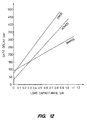
- FIG. 12 is a graph illustrating the performance in comparison to regular CMOS and BiNMOS.
- CMOS logic circuit since only some of the MOS transistors of a CMOS logic circuit are selectively lowered, the speed performance of the CMOS circuit can be improved while minimizing the resulting increase in power dissipation.
- CMOS circuits can only be scaled down to about 2 volts.
- the CMOS circuits described herein can scale down to at least 1 volt.
- the embodiments are particularly scalable because the output is either pulled-up to a rail or pulled-down to a rail, irrespective of V DD .
- CMOS circuits are only slightly more complicated than that required for conventional CMOS circuits.
- two extra implant steps are required for the channel implant of the two low Vt devices (one implant for each device).
- FIG. 3 is a schematic diagram of a CMOS inverter 56 embodying the invention.
- the CMOS inverter 56 includes a low threshold voltage (LVt) PMOS transistor 58 and a normal threshold voltage (NVt) NMOS transistor 60.
- the LVt PMOS transistor 58 has a source terminal 62 connected to a power terminal 64, a gate terminal 66 connected to an input terminal 68, and a drain terminal 70 connected to an output terminal 72.
- the NVt NMOS transistor 60 has a drain terminal 74 connected to the output terminal 72, a gate terminal 76 connected to the input terminal 68, and a source terminal 78 connected to a ground terminal 80.
- the LVt PMOS transistor 58 When the input signal on the input terminal 68 is "high”, the LVt PMOS transistor 58 is off and the NVt NMOS transistor 60 is on, thereby pulling down the output signal on the output terminal 72 to ground 80.
- the pull-down performance of the NVt NMOS transistor 60 is the same as with conventional CMOS.
- the NVt NMOS transistor 60 is off and the LVt PMOS transistor 58 is on, thereby pulling up the output signal on the output terminal 72 to the power supply voltage using a high drive current.
- the CMOS inverter 56 is configured in accordance with the first embodiment. However, those skilled in the art will readily recognize that the CMOS inverter 56 can also be configured in accordance with the second embodiment.
- FIG. 4 is a schematic diagram of a CMOS NAND circuit 82 embodying the invention.
- the CMOS NAND circuit 82 includes four transistors 84-90 as does a conventional CMOS NAND circuit, but the threshold voltages of some of the transistors is low to improve the speed performance of the circuit 82.
- the LVt PMOS transistor 84 has a source terminal 92 connected to a power terminal 94, a gate terminal 96 connected to a first input terminal 98 to receive input signal A, and a drain terminal 100 connected to an output terminal 102.
- the LVt PMOS transistor 86 has a source terminal 104 connected to the power terminal 94, a gate terminal 106 connected to a second input terminal 108 to receive input signal B, and a drain terminal 110 connected to the output terminal 102.
- the LVt NMOS transistor 88 has a drain terminal 112 connected to the output terminal 102, a gate terminal 114 connected to the first input terminal 98 to receive the input signal A, and a source terminal 116.
- the NVt NMOS transistor 90 has a drain terminal 118 connected to the source terminal 116 of the LVt NMOS transistor 88, a gate terminal 120 connected to the second input terminal 108 to receive the input signal B, and a source terminal 122 connected to ground 124.
- PMOS transistors 84, 86 and NMOS transistor 88 are illustrated as being low Vt devices, and NMOS transistor 90 is illustrated as being normal or standard Vt device.
- the LVt PMOS transistors 84 and 86 operate to pull-up the output signal at high speed.
- the NMOS transistors 88 and 90 operate to pull-down the output signal.
- the CMOS NAND circuit 82 was designed to improve its performance while minimizing power loss.
- PMOS transistors 84 and 86 were selected for low Vt so improve the pull-up speed of the circuit 82.
- NMOS for the same magnitude Vt
- the NMOS transistor 88 is also a low Vt transistor.
- NMOS transistor 88 Using a low Vt NMOS transistor 88 would, for example, be advantageous in cases where the rate of change of input signal A is substantially greater than the rate of change of the input signal B because the speed gain obtained for the pull-down would out weigh the increase in power loss by the NMOS transistor 88.
- CMOS circuits can be improved over that conventionally available (with conventional Vt) by a factor which is believed to be between about 25 % to 45 %, yet increasing the power loss only to the extend necessary.
- Vt PMOS and low Vt NMOS can be used in speed critical paths, thereby improving the speed performance of the CMOS circuit. Further, in non-critical paths the normal (standard) Vt PMOS and normal (standard) Vt NMOS is used to minimize power loss because normal Vt transistors have less power dissipation that the low Vt transistors.
- FIG. 5 is a top view of an integrated circuit (IC) chip 126 containing low and standard threshold voltage CMOS transistors which are used to implement a logic circuit.
- the chip 126 includes LVT NMOS regions 128, NVt NMOS regions 130, LVt PMOS regions 132, and NVt PMOS regions 134.
- the IC chip 126 can be an ASIC, a PLA, a gate array, an IC of standard cells, or a standard or custom designed IC.
- Each of the regions 128-134 includes CMOS technology, namely MOS transistors.
- the logic circuit formed using the chip 126 would make use of the various regions 128-134 to improve the speed/power dissipation tradeoff.
- low Vt transistors or logic devices formed in the LVt NMOS region 128 and/or LVt PMOS region 132 would be used in speed critical paths in place of normal threshold transistors or devices, whereas normal Vt transistors or logic devices formed in the NVt NMOS region 130 and/or NVt PMOS region 134 would be used in non-critical speed paths.
- FIG. 6 is a top view of a circuit 136 containing a normal threshold voltage (NVt) logic circuit 138 and a low threshold voltage (LVt) logic circuit 140.
- the circuit 136 is implemented using both the low Vt logic circuit 138 and the normal Vt logic circuit 140.
- the logic circuits 138-140 contain one or more logic devices (AND, OR, NOR, inverter, etc.).
- FIG. 7 is a schematic diagram of an exemplary embodiment of the circuit 136 of FIG. 6.
- the NVt logic circuit 138 includes an AND gate 142
- the LVt logic circuit 140 includes an inverter 144.
- the circuit 136 receives input signals IN1 and IN2 at the input terminals of the AND gate 142, forwards the result to the input terminal of the inverter 144, and outputs the final result as an output signal (OUT).
- the mixture of the NVt and LVt logic circuits enables the circuit 136 to improve speed performance of the circuit 136 where needed, while at the same time minimizing the power dissipation.
- speed performance can be improved where needed without unnecessarily increasing power dissipation.
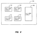
- FIG. 8 is a top view of a complex circuit 146 containing a plurality of logic circuits having either a normal threshold voltage or a low threshold voltage.
- the complex circuit 146 includes a first NVt logic circuit 148, a second NVt logic circuit 150, a third NVt logic circuit 152, a first LVt logic circuit 154, and a second LVt logic circuit 156.
- the selective introduction of LVt logic circuits 154, 156 into the design of the complex circuit 146 operates to improve the speed performance of the complex circuit 146 without substantially increasing power dissipation.
- FIGS. 9 and 10 Examples of two common circuits designed with both normal and low voltage threshold logic circuits are provided in FIGS. 9 and 10.
- FIG. 9 is a block diagram of a high-speed cache memory 158 embodying the invention.
- the cache memory 158 includes an array of cache memory storage cells 160, an address decoder 162, and a plurality of sense amplifiers 164.
- the speed of the cache memory 158 is improved by using low Vt CMOS transistors in the address decoder 162 and the sense amplifiers 164.
- the many hundreds of thousand transistors of the memory storage cells 160 are kept at normal Vt because their speed is less critical than for the decoder 162 or sense amplifiers 164 and because to make the memory cells 160 low Vt would result in substantial power dissipation.
- the speed of the memory cells 160 is not critical enough to warrant the increase in power dissipation and, in addition, leakage current must be kept low in memory arrays.
- FIG. 10 is a block diagram of a floating-point arithmetic unit 166 designed with both low threshold voltage circuits and normal threshold voltage circuits.
- the floating-point arithmetic unit 166 includes a register file array 168, sense amplifiers 170, a multiplication unit 172, an align shifter 174, a 3:2 carry save adder 176, a carry propagate adder 178 and a latch 180.
- a register file array 168 sense amplifiers 170
- a multiplication unit 172 a multiplication unit 172
- an align shifter 174 a 3:2 carry save adder 176
- a carry propagate adder 178 and a latch 180.
- the sense amplifiers 170, the multiplication unit 172, the align shifter 174, the carry save adder 176, the carry propagate adder 178 and the latch 180 are all implemented using low Vt to increase the speed on the arithmetic unit 166, and the register file array 168 is implemented in normal Vt because its speed is not as critical.
- the basic operation of such an arithmetic unit 166 follows that of the arithmetic unit disclosed in U.S. Patent No. 4,999,802.
- the user when designing a circuit using CMOS technology, one can select whether the pieces or parts of the design should be implemented in normal Vt or low Vt. For example, if a computer-aided-design (CAD) system is used in designing the circuit, the user simply selects not only the logic devices (e.g., OR gate, NOR gate, AND gate, NAND gate, inverter, buffer, tri-state gate, or the like) to be used but also the threshold voltage to be used in the logic devices (see FIG. 11 discussed below). Namely, the voltage threshold to be used can be normal Vt or low Vt. The low Vt is selected for the most speed critical paths to the extent practical given that low Vt increases power dissipation. For example, if speed is critical in a certain portion of the circuit, a LVt logic device is used, whereas in another portion of the circuit where speed is not critical, a NVt logic device is used.
- CAD computer-aided-design
- the low threshold voltage of the MOS transistors is within the range of about 0.1 - 0.3 volts and the standard (or normal) threshold voltage of the MOS transistors is within the range of about 0.4 - 1.0 volts.
- the standard threshold of the MOS transistors is within the range of about 0.1 - 0.2 volts which is already relatively low; hence, the altered threshold is increased (instead of lowered) to about 0.3 - 0.4 volts.
- the speed/power dissipation is controlled by using the higher threshold voltage MOS transistors where slower speed can be tolerated, thereby decreasing power dissipation of the CMOS circuit.
- FIG. 11 is a block diagram of a CAD system 182 which provides a method of designing CMOS logic circuits of the type described above.
- the CAD design system includes a CAD system controller 184 and a display screen 186.
- the method would begin by identifying a logic element for forming a portion of the circuit.
- the portion of the circuit could represent a single transistor or a standard logic device.
- the method determines whether the logic element identified is within a speed critical path in the logic circuit being designed. If it is, then a low threshold voltage construction of the logic element is selected. Typically, the designer would select the low threshold construction from a menu 188 of logic devices 190 - 212 produced on the display screen 188 by the CAD system controller 184. For example, if a NAND gate is the identified logic function desired and its determined to be in a speed critical path, then the designer can choose from a low Vt construction 204 and a normal Vt construction 202.
- the designer might want to choose a partially low Vt such as illustrated in FIG. 4.
- a normal threshold voltage construction of the logic element is selected.
- the designer might want to choose a high Vt instead of the normal Vt, for example when the normal Vt is already low (e.g., low power supply voltage situation).
- FIG. 12 is a graph illustrating the performance advantage of the circuits described herein in comparison to regular CMOS and BiNMOS circuits.
- the horizontal axis represents load capacitance and the vertical axis represents gate delay; the reference ACMOS representing adaptive CMOS.
- the adaptive CMOS ACMOS
- ACMOS is actually faster (i.e., lower gate delay) than BiNMOS at load capacitances less than about 0.2 pf.
Landscapes
- Engineering & Computer Science (AREA)
- Computer Hardware Design (AREA)
- Physics & Mathematics (AREA)
- General Engineering & Computer Science (AREA)
- Theoretical Computer Science (AREA)
- General Physics & Mathematics (AREA)
- Geometry (AREA)
- Evolutionary Computation (AREA)
- Computing Systems (AREA)
- Mathematical Physics (AREA)
- Logic Circuits (AREA)
- Metal-Oxide And Bipolar Metal-Oxide Semiconductor Integrated Circuits (AREA)
- Memory System Of A Hierarchy Structure (AREA)
Applications Claiming Priority (2)
| Application Number | Priority Date | Filing Date | Title |
|---|---|---|---|
| US15393793A | 1993-11-17 | 1993-11-17 | |
| US153937 | 1993-11-17 |
Publications (2)
| Publication Number | Publication Date |
|---|---|
| EP0653843A2 true EP0653843A2 (de) | 1995-05-17 |
| EP0653843A3 EP0653843A3 (de) | 1996-05-01 |
Family
ID=22549328
Family Applications (1)
| Application Number | Title | Priority Date | Filing Date |
|---|---|---|---|
| EP94308379A Withdrawn EP0653843A3 (de) | 1993-11-17 | 1994-11-14 | CMOS Schaltungen mit adaptiver Spannungsschwelle. |
Country Status (3)
| Country | Link |
|---|---|
| US (1) | US5629638A (de) |
| EP (1) | EP0653843A3 (de) |
| JP (1) | JPH07202679A (de) |
Cited By (5)
| Publication number | Priority date | Publication date | Assignee | Title |
|---|---|---|---|---|
| EP1217662A1 (de) * | 2000-12-21 | 2002-06-26 | Universite Catholique De Louvain | Basisbausteine mit extrem geringer Leistung und ihre Verwendung |
| US6611680B2 (en) | 1997-02-05 | 2003-08-26 | Telefonaktiebolaget Lm Ericsson (Publ) | Radio architecture |
| EP1058386A4 (de) * | 1997-12-26 | 2006-05-31 | Hitachi Ltd | Integrierte halbleiterschaltung mit aufzeichnungsmedium gespeichert mit einer zellenbibliothek und verfahren zum entwurf einer integrierten halbleiterschaltung |
| US9787294B2 (en) | 2010-05-21 | 2017-10-10 | Semiconductor Energy Laboratory Co., Ltd. | Pulse converter circuit |
| CN114388494A (zh) * | 2020-10-06 | 2022-04-22 | 三星电子株式会社 | 半导体器件 |
Families Citing this family (22)
| Publication number | Priority date | Publication date | Assignee | Title |
|---|---|---|---|---|
| JP3173408B2 (ja) * | 1997-03-13 | 2001-06-04 | 日本電気株式会社 | 信号多重化回路 |
| US6078195A (en) * | 1997-06-03 | 2000-06-20 | International Business Machines Corporation | Logic blocks with mixed low and regular Vt MOSFET devices for VLSI design in the deep sub-micron regime |
| KR100244778B1 (ko) * | 1997-07-19 | 2000-02-15 | 윤종용 | 정상 동작중인 시스템에 보드를 실장 또는 탈장하는 회로 |
| KR100294695B1 (ko) * | 1998-01-13 | 2001-07-12 | 김영환 | 저전력씨모스회로 |
| JP3415444B2 (ja) * | 1998-06-12 | 2003-06-09 | Necエレクトロニクス株式会社 | クロック制御方法および回路 |
| US6333230B1 (en) | 2000-05-15 | 2001-12-25 | International Business Machines Corporation | Scalable high-voltage devices |
| JP2002118176A (ja) * | 2000-10-05 | 2002-04-19 | Nec Corp | 半導体装置 |
| JP3928937B2 (ja) * | 2002-05-24 | 2007-06-13 | シャープ株式会社 | 半導体集積回路 |
| US7103857B2 (en) * | 2003-12-09 | 2006-09-05 | International Business Machines Corporation | Method and latch circuit for implementing enhanced performance with reduced quiescent power dissipation using mixed threshold CMOS devices |
| JP2007109983A (ja) * | 2005-10-14 | 2007-04-26 | Matsushita Electric Ind Co Ltd | 半導体集積回路装置、電子機器及び半導体集積回路装置の製造方法 |
| US20070106964A1 (en) * | 2005-11-10 | 2007-05-10 | Meindl James D | Optimized microchip and related methods |
| US7893723B2 (en) * | 2007-12-29 | 2011-02-22 | Texas Instruments Incorporated | Minimizing leakage in logic designs |
| US8957398B2 (en) | 2010-12-22 | 2015-02-17 | Easic Corporation | Via-configurable high-performance logic block involving transistor chains |
| US8856712B2 (en) * | 2012-08-13 | 2014-10-07 | Sandisk Technologies Inc. | Optimized flip-flop device with standard and high threshold voltage MOS devices |
| KR102002380B1 (ko) * | 2012-10-10 | 2019-07-23 | 삼성전자 주식회사 | 반도체 장치 및 그 제조 방법 |
| WO2015099788A1 (en) * | 2013-12-27 | 2015-07-02 | Intel Corporation | Dual voltage asymmetric memory c |
| US10191106B2 (en) * | 2015-09-25 | 2019-01-29 | Qualcomm Incorporated | Techniques to identify a process corner |
| CN108075767A (zh) * | 2016-11-11 | 2018-05-25 | 恩智浦美国有限公司 | 低功耗cmos缓冲电路 |
| US11626875B2 (en) * | 2018-04-20 | 2023-04-11 | Texas Instruments Incorporated | Stress reduction on stacked transistor circuits |
| US11831309B2 (en) | 2018-04-20 | 2023-11-28 | Texas Instruments Incorporated | Stress reduction on stacked transistor circuits |
| US11081167B1 (en) * | 2020-06-26 | 2021-08-03 | Sandisk Technologies Llc | Sense amplifier architecture for low supply voltage operations |
| CN111898334B (zh) * | 2020-08-04 | 2022-02-01 | 深圳比特微电子科技有限公司 | 用于系统级芯片设计的标准单元及应用其的数据处理单元、运算芯片和计算设备 |
Family Cites Families (15)
| Publication number | Priority date | Publication date | Assignee | Title |
|---|---|---|---|---|
| US4250406A (en) * | 1978-12-21 | 1981-02-10 | Motorola, Inc. | Single clock CMOS logic circuit with selected threshold voltages |
| US4489246A (en) * | 1980-12-24 | 1984-12-18 | Fujitsu Limited | Field effect transistor logic circuit having high operating speed and low power consumption |
| EP0058958B1 (de) * | 1981-02-25 | 1986-10-29 | Kabushiki Kaisha Toshiba | Komplementäre MOSFET-Logikschaltung |
| US4463273A (en) * | 1981-10-26 | 1984-07-31 | Rca Corporation | Electronic circuits and structures employing enhancement and depletion type IGFETs |
| US4612461A (en) * | 1984-02-09 | 1986-09-16 | Motorola, Inc. | High speed input buffer having substrate biasing to increase the transistor threshold voltage for level shifting |
| US4595845A (en) * | 1984-03-13 | 1986-06-17 | Mostek Corporation | Non-overlapping clock CMOS circuit with two threshold voltages |
| US4808854A (en) * | 1987-03-05 | 1989-02-28 | Ltv Aerospace & Defense Co. | Trinary inverter |
| JP2553632B2 (ja) * | 1988-05-16 | 1996-11-13 | 松下電器産業株式会社 | バイモス型論理回路 |
| US5057715A (en) * | 1988-10-11 | 1991-10-15 | Intel Corporation | CMOS output circuit using a low threshold device |
| US4956691A (en) * | 1989-03-24 | 1990-09-11 | Delco Electronics Corporation | NMOS driver circuit for CMOS circuitry |
| US5017811A (en) * | 1989-10-27 | 1991-05-21 | Rockwell International Corporation | CMOS TTL input buffer using a ratioed inverter with a threshold voltage adjusted N channel field effect transistor |
| US5091324A (en) * | 1990-08-10 | 1992-02-25 | Advanced Micro Devices, Inc. | Process for producing optimum intrinsic, long channel, and short channel mos devices in vlsi structures |
| US5200921A (en) * | 1990-09-20 | 1993-04-06 | Fujitsu Limited | Semiconductor integrated circuit including P-channel MOS transistors having different threshold voltages |
| US5150186A (en) * | 1991-03-06 | 1992-09-22 | Micron Technology, Inc. | CMOS output pull-up driver |
| US5132567A (en) * | 1991-04-18 | 1992-07-21 | International Business Machines Corporation | Low threshold BiCMOS circuit |
-
1994
- 1994-11-14 EP EP94308379A patent/EP0653843A3/de not_active Withdrawn
- 1994-11-17 JP JP6308215A patent/JPH07202679A/ja active Pending
-
1995
- 1995-10-12 US US08/542,235 patent/US5629638A/en not_active Expired - Lifetime
Cited By (8)
| Publication number | Priority date | Publication date | Assignee | Title |
|---|---|---|---|---|
| US6611680B2 (en) | 1997-02-05 | 2003-08-26 | Telefonaktiebolaget Lm Ericsson (Publ) | Radio architecture |
| US6973290B2 (en) | 1997-02-05 | 2005-12-06 | Telefonaktiebolaget L M Ericsson (Publ) | Radio architecture |
| EP1058386A4 (de) * | 1997-12-26 | 2006-05-31 | Hitachi Ltd | Integrierte halbleiterschaltung mit aufzeichnungsmedium gespeichert mit einer zellenbibliothek und verfahren zum entwurf einer integrierten halbleiterschaltung |
| EP1217662A1 (de) * | 2000-12-21 | 2002-06-26 | Universite Catholique De Louvain | Basisbausteine mit extrem geringer Leistung und ihre Verwendung |
| WO2002050911A1 (en) * | 2000-12-21 | 2002-06-27 | Universite Catholique De Louvain | Ultra-low power basic blocks and their uses |
| US9787294B2 (en) | 2010-05-21 | 2017-10-10 | Semiconductor Energy Laboratory Co., Ltd. | Pulse converter circuit |
| CN114388494A (zh) * | 2020-10-06 | 2022-04-22 | 三星电子株式会社 | 半导体器件 |
| CN114388494B (zh) * | 2020-10-06 | 2026-01-16 | 三星电子株式会社 | 半导体器件 |
Also Published As
| Publication number | Publication date |
|---|---|
| US5629638A (en) | 1997-05-13 |
| EP0653843A3 (de) | 1996-05-01 |
| JPH07202679A (ja) | 1995-08-04 |
Similar Documents
| Publication | Publication Date | Title |
|---|---|---|
| US5629638A (en) | Adaptive threshold voltage CMOS circuits | |
| US6952114B2 (en) | Apparatus and methods for silicon-on-insulator transistors in programmable logic devices | |
| US7800405B2 (en) | Passgate structures for use in low-voltage applications | |
| EP1024597B1 (de) | Ausgangsschaltung zur Verwendung in einer integrierten Halbleiterschaltung | |
| EP0480201A1 (de) | Chip-Ausgangsschnittstellenschaltung | |
| EP0239059B1 (de) | Logische Schaltung | |
| EP0449251B1 (de) | Ausgangsschaltung | |
| US5068548A (en) | Bicmos logic circuit for basic applications | |
| JPH04299567A (ja) | セットアップ時間の短い低電力cmosバスレシーバ | |
| US6768335B1 (en) | Integrated circuit multiplexer including transistors of more than one oxide thickness | |
| US6111455A (en) | Method for controlling delays in silicon on insulator circuits | |
| JPH10508175A (ja) | 不揮発性メモリ集積回路における高電圧切換え用高電圧レベルシフタ | |
| US7292065B2 (en) | Enhanced passgate structures for reducing leakage current | |
| US6252426B1 (en) | High speed logic family | |
| US7417454B1 (en) | Low-swing interconnections for field programmable gate arrays | |
| US6518796B1 (en) | Dynamic CMOS circuits with individually adjustable noise immunity | |
| EP1454414B1 (de) | Schnelle ausgangsschaltung geeignet für geringe spannungen | |
| US7321236B2 (en) | Apparatus and methods for programmable logic devices with improved performance characteristics | |
| US6563367B1 (en) | Interconnection switch structures | |
| US5694055A (en) | Zero static power programmable logic cell | |
| JPH0795040A (ja) | ノイズ減少回路を有する出力バッファ回路 | |
| US6366123B1 (en) | Input buffer circuit for low power application | |
| US5719506A (en) | Fast signal path for programmable logic device | |
| GB2245098A (en) | Logic circuits | |
| GB2296586A (en) | Transition assist for fast row driver-decoder |
Legal Events
| Date | Code | Title | Description |
|---|---|---|---|
| PUAI | Public reference made under article 153(3) epc to a published international application that has entered the european phase |
Free format text: ORIGINAL CODE: 0009012 |
|
| AK | Designated contracting states |
Kind code of ref document: A2 Designated state(s): DE FR GB NL |
|
| PUAL | Search report despatched |
Free format text: ORIGINAL CODE: 0009013 |
|
| AK | Designated contracting states |
Kind code of ref document: A3 Designated state(s): DE FR GB NL |
|
| 17P | Request for examination filed |
Effective date: 19960916 |
|
| 17Q | First examination report despatched |
Effective date: 19970611 |
|
| STAA | Information on the status of an ep patent application or granted ep patent |
Free format text: STATUS: THE APPLICATION IS DEEMED TO BE WITHDRAWN |
|
| 18D | Application deemed to be withdrawn |
Effective date: 19990812 |