EP0665579A1 - Method of fabricating gate stack having a reduced height - Google Patents
Method of fabricating gate stack having a reduced height Download PDFInfo
- Publication number
- EP0665579A1 EP0665579A1 EP94309348A EP94309348A EP0665579A1 EP 0665579 A1 EP0665579 A1 EP 0665579A1 EP 94309348 A EP94309348 A EP 94309348A EP 94309348 A EP94309348 A EP 94309348A EP 0665579 A1 EP0665579 A1 EP 0665579A1
- Authority
- EP
- European Patent Office
- Prior art keywords
- layer
- patterned
- metal
- oxide
- etching
- Prior art date
- Legal status (The legal status is an assumption and is not a legal conclusion. Google has not performed a legal analysis and makes no representation as to the accuracy of the status listed.)
- Withdrawn
Links
Images
Classifications
-
- H—ELECTRICITY
- H10—SEMICONDUCTOR DEVICES; ELECTRIC SOLID-STATE DEVICES NOT OTHERWISE PROVIDED FOR
- H10D—INORGANIC ELECTRIC SEMICONDUCTOR DEVICES
- H10D84/00—Integrated devices formed in or on semiconductor substrates that comprise only semiconducting layers, e.g. on Si wafers or on GaAs-on-Si wafers
- H10D84/01—Manufacture or treatment
- H10D84/0123—Integrating together multiple components covered by H10D12/00 or H10D30/00, e.g. integrating multiple IGBTs
- H10D84/0126—Integrating together multiple components covered by H10D12/00 or H10D30/00, e.g. integrating multiple IGBTs the components including insulated gates, e.g. IGFETs
- H10D84/0165—Integrating together multiple components covered by H10D12/00 or H10D30/00, e.g. integrating multiple IGBTs the components including insulated gates, e.g. IGFETs the components including complementary IGFETs, e.g. CMOS devices
- H10D84/0172—Manufacturing their gate conductors
-
- H—ELECTRICITY
- H10—SEMICONDUCTOR DEVICES; ELECTRIC SOLID-STATE DEVICES NOT OTHERWISE PROVIDED FOR
- H10D—INORGANIC ELECTRIC SEMICONDUCTOR DEVICES
- H10D64/00—Electrodes of devices having potential barriers
- H10D64/01—Manufacture or treatment
- H10D64/013—Manufacture or treatment of electrodes having a conductor capacitively coupled to a semiconductor by an insulator
- H10D64/01302—Manufacture or treatment of electrodes having a conductor capacitively coupled to a semiconductor by an insulator the insulator being formed after the semiconductor body, the semiconductor being silicon
- H10D64/01304—Manufacture or treatment of electrodes having a conductor capacitively coupled to a semiconductor by an insulator the insulator being formed after the semiconductor body, the semiconductor being silicon characterised by the conductor
- H10D64/01326—Aspects related to lithography, isolation or planarisation of the conductor
-
- H—ELECTRICITY
- H10—SEMICONDUCTOR DEVICES; ELECTRIC SOLID-STATE DEVICES NOT OTHERWISE PROVIDED FOR
- H10D—INORGANIC ELECTRIC SEMICONDUCTOR DEVICES
- H10D84/00—Integrated devices formed in or on semiconductor substrates that comprise only semiconducting layers, e.g. on Si wafers or on GaAs-on-Si wafers
- H10D84/80—Integrated devices formed in or on semiconductor substrates that comprise only semiconducting layers, e.g. on Si wafers or on GaAs-on-Si wafers characterised by the integration of at least one component covered by groups H10D12/00 or H10D30/00, e.g. integration of IGFETs
- H10D84/82—Integrated devices formed in or on semiconductor substrates that comprise only semiconducting layers, e.g. on Si wafers or on GaAs-on-Si wafers characterised by the integration of at least one component covered by groups H10D12/00 or H10D30/00, e.g. integration of IGFETs of only field-effect components
- H10D84/83—Integrated devices formed in or on semiconductor substrates that comprise only semiconducting layers, e.g. on Si wafers or on GaAs-on-Si wafers characterised by the integration of at least one component covered by groups H10D12/00 or H10D30/00, e.g. integration of IGFETs of only field-effect components of only insulated-gate FETs [IGFET]
- H10D84/85—Complementary IGFETs, e.g. CMOS
- H10D84/853—Complementary IGFETs, e.g. CMOS comprising FinFETs
-
- Y—GENERAL TAGGING OF NEW TECHNOLOGICAL DEVELOPMENTS; GENERAL TAGGING OF CROSS-SECTIONAL TECHNOLOGIES SPANNING OVER SEVERAL SECTIONS OF THE IPC; TECHNICAL SUBJECTS COVERED BY FORMER USPC CROSS-REFERENCE ART COLLECTIONS [XRACs] AND DIGESTS
- Y10—TECHNICAL SUBJECTS COVERED BY FORMER USPC
- Y10S—TECHNICAL SUBJECTS COVERED BY FORMER USPC CROSS-REFERENCE ART COLLECTIONS [XRACs] AND DIGESTS
- Y10S148/00—Metal treatment
- Y10S148/105—Masks, metal
Definitions
- This invention generally relates to the fabrication of integrated circuits, and more particularly to a method for fabricating multilayer gate stacks in an integrated circuit.
- a gate stack or multilayer structure is typically used as gate electrodes or interconnects in MOS and CMOS integrated circuits.
- One gate stack that has been proposed consists of layers of doped polysilicon or amorphous silicon, tungsten silicide (WSi2), and silicon dioxide (SiO2).
- the oxide layer is patterned and used as a hard mask to subsequently etch the underlying polysilicon and silicide layers. After the gate stack is patterned in this manner, the oxide hard mask is retained in the final gate structure. Consequently, the total height of the gate stack includes the height of the oxide mask layer, which contributes as much as 30 % to the total height of the gate stack.
- the oxide mask layer cannot be removed after the gate stack is patterned since its removal would also thin down the field oxide layer and thus adversely affect isolation between adjacent transistors. Because both the oxide mask and the field oxide layer are oxides, the etching selectivity between them is poor. Thinning down the field oxide layer can also cause significant damage which can result in defects in the integrated circuit.
- a reduction in the height of a gate stack is achieved in accordance with the present invention by removing the silicon dioxide mask layer, leaving only a metal layer and a polysilicon layer in the final gate stack.
- the oxide hard mask used to pattern the metal layer may be removed since the polysilicon layer is used to protect the field oxide layer from the etchant used to selectively remove the oxide mask.
- the etching is completed using the patterned metal as a mask to etch the polysilicon layer down to the gate oxide, without thinning down the field oxide layer.
- Advantages of the process include reduction of topography, process uniformity, and simplicity as compared to the conventional gate fabrication processes.
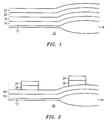
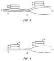
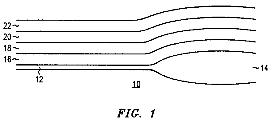
- FIGS. 1-4 illustrate cross-sectional views of an integrated circuit at successive stages of its fabrication in accordance with the invention.
- the fabrication of the gate stack in accordance with the invention begins with a silicon substrate 10 on which is formed, as is conventional, a gate oxide layer 12 and a surrounding field oxide layer 14, the latter providing isolation between adjacent transistors.
- a layer of doped polysilicon 16 or amorphous silicon is formed over the oxide layers 12, 14 and a refractory metal layer 18 such as of tungsten silicide (WSi2) or titanium nitride (TiN) silicide is formed over polysilicon layer 16.
- WSi2 tungsten silicide
- TiN titanium nitride
- a silicon dioxide layer 20 is formed over metal layer 18 and a layer of photoresist 22 is formed over the oxide layer 20. Layers 16 and 18 and 20 may each be about 1000 ⁇ in thickness.
- the photo-resist layer 22 is patterned by a photolithograph process to form photoresist masks 24, and the underlying silicon oxide layer 20 is etched away to leave a patterned layer 26 of silicon dioxide beneath the patterned photoresist 24.
- the photoresist masks 24 are removed in a conventional manner.
- the now-exposed patterned oxide layer 26 is employed as a hard mask to etch away the exposed metal layer 18 to leave a patterned layer of metal 28, and also partly to etch away the exposed polysilicon layer 16.
- etching the metal layer can stop upon reaching the upper surface of the polysilicon layer. A portion of the polysilicon layer 16 will be etched away by an amount determined by the etching selectivity.
- the oxide hard mask 24 is removed completely by a known technique, as shown in Fig. 4, which may include either dry etching or wet etching. During the removal of the hard mask, the remaining polysilicon layer 16 is of sufficient thickness to protect the field oxide layer 14 from the etchant used in this step of the process.
- the now-exposed patterned metal silicide layer 28 is then used as a hard mask for etching away the remaining polysilicon layer 24, as shown in Fig. 4, to form a patterned polysilicon layer 30 to the gate oxide layer 12. This etching step can be safely performed without attacking the gate and field oxide layers because the etching selectivity of the polysilicon layer to the oxide is high, about 20 to 1.
- the process produces a gate stack 32, comprising the patterned polysilicon layer 30 and the patterned metal layer 28, as opposed to a conventional gate stack, which also includes an overlying oxide layer.
- the gate stack fabricated in this manner simplifies the back-end process of wiring and the like as a result of the reduced height of the gate stack.
- the gate stack as shown in Fig. 4, may constitute the gate electrode of an MOS transistor or an interconnect located in the field region.
Landscapes
- Drying Of Semiconductors (AREA)
- Electrodes Of Semiconductors (AREA)
- Insulated Gate Type Field-Effect Transistor (AREA)
- Internal Circuitry In Semiconductor Integrated Circuit Devices (AREA)
- Metal-Oxide And Bipolar Metal-Oxide Semiconductor Integrated Circuits (AREA)
Abstract


Description
- This invention generally relates to the fabrication of integrated circuits, and more particularly to a method for fabricating multilayer gate stacks in an integrated circuit.
- A gate stack or multilayer structure is typically used as gate electrodes or interconnects in MOS and CMOS integrated circuits. One gate stack that has been proposed consists of layers of doped polysilicon or amorphous silicon, tungsten silicide (WSi₂), and silicon dioxide (SiO2). The oxide layer is patterned and used as a hard mask to subsequently etch the underlying polysilicon and silicide layers. After the gate stack is patterned in this manner, the oxide hard mask is retained in the final gate structure. Consequently, the total height of the gate stack includes the height of the oxide mask layer, which contributes as much as 30 % to the total height of the gate stack.
- The oxide mask layer cannot be removed after the gate stack is patterned since its removal would also thin down the field oxide layer and thus adversely affect isolation between adjacent transistors. Because both the oxide mask and the field oxide layer are oxides, the etching selectivity between them is poor. Thinning down the field oxide layer can also cause significant damage which can result in defects in the integrated circuit.
- Different ways of reducing gate-stack height have been attempted, but have not proven to be successful in terms of cost effectiveness as a result of low yield. One approach has involved the use of a BPTEOS hard mask with a special wet etch. One problem with the use of BPTEOS as a hard mask has been an attack on the field oxide layer due to the increase in the wet etch rate during the removal of the hard mask, especially at the edges of the field oxide, where the wet etch rate is especially high. A further problem in this approach is the tendency of boron and phosphorous impurities in the oxide to diffuse rapidly.
- Previous proposals to avoid the use of oxide hard mask have failed to control the transistor dimensions with the required precision and suffer from poor linewidth control as a result of deposits formed on the patterned vertical sidewalls. In the larger pattern geometries, deposits of 100 to 200 Angstroms did not present serious problems; however, in the new generation of smaller pattern geometries, the resultant poor linewidth control may result in defective transistors or low yield.
- It is an object of the present invention to provide a process of fabricating an integrated circuit with a gate-stack structure having reduced topography.
- It is another object of the invention to provide a process for fabricating integrated circuits in which the hard oxide mask of a gate stack structure can be removed by a single and reliable process.
- A reduction in the height of a gate stack is achieved in accordance with the present invention by removing the silicon dioxide mask layer, leaving only a metal layer and a polysilicon layer in the final gate stack. The oxide hard mask used to pattern the metal layer may be removed since the polysilicon layer is used to protect the field oxide layer from the etchant used to selectively remove the oxide mask. The etching is completed using the patterned metal as a mask to etch the polysilicon layer down to the gate oxide, without thinning down the field oxide layer. Advantages of the process include reduction of topography, process uniformity, and simplicity as compared to the conventional gate fabrication processes.
- The foregoing features of the present invention can be more fully understood from the following detailed description of a specific illustrative embodiment thereof, presented hereinbelow in conjunction with the accompanying drawing, in which FIGS. 1-4 illustrate cross-sectional views of an integrated circuit at successive stages of its fabrication in accordance with the invention.
- Referring to FIG. 1, the fabrication of the gate stack in accordance with the invention begins with a
silicon substrate 10 on which is formed, as is conventional, agate oxide layer 12 and a surroundingfield oxide layer 14, the latter providing isolation between adjacent transistors. A layer of dopedpolysilicon 16 or amorphous silicon is formed over theoxide layers refractory metal layer 18 such as of tungsten silicide (WSi₂) or titanium nitride (TiN) silicide is formed overpolysilicon layer 16. Asilicon dioxide layer 20 is formed overmetal layer 18 and a layer ofphotoresist 22 is formed over theoxide layer 20.Layers - Next, as shown in Fig. 2, as is conventional, the photo-
resist layer 22 is patterned by a photolithograph process to formphotoresist masks 24, and the underlyingsilicon oxide layer 20 is etched away to leave a patternedlayer 26 of silicon dioxide beneath the patternedphotoresist 24. - Thereafter, as shown in Fig. 3, the
photoresist masks 24 are removed in a conventional manner. In accordance with the present invention, the now-exposed patternedoxide layer 26 is employed as a hard mask to etch away the exposedmetal layer 18 to leave a patterned layer ofmetal 28, and also partly to etch away the exposedpolysilicon layer 16. - If the metal layer and the polysilicon layer have significant etching selectivity, etching the metal layer can stop upon reaching the upper surface of the polysilicon layer. A portion of the
polysilicon layer 16 will be etched away by an amount determined by the etching selectivity. - Following the selective etching of the metal layer, the oxide
hard mask 24 is removed completely by a known technique, as shown in Fig. 4, which may include either dry etching or wet etching. During the removal of the hard mask, theremaining polysilicon layer 16 is of sufficient thickness to protect thefield oxide layer 14 from the etchant used in this step of the process. The now-exposed patternedmetal silicide layer 28 is then used as a hard mask for etching away theremaining polysilicon layer 24, as shown in Fig. 4, to form apatterned polysilicon layer 30 to thegate oxide layer 12. This etching step can be safely performed without attacking the gate and field oxide layers because the etching selectivity of the polysilicon layer to the oxide is high, about 20 to 1. - As shown in Fig. 4, the process produces a
gate stack 32, comprising the patternedpolysilicon layer 30 and the patternedmetal layer 28, as opposed to a conventional gate stack, which also includes an overlying oxide layer. The gate stack fabricated in this manner simplifies the back-end process of wiring and the like as a result of the reduced height of the gate stack. The gate stack, as shown in Fig. 4, may constitute the gate electrode of an MOS transistor or an interconnect located in the field region. - The above-described process is merely illustrative of the principles of the present invention. Numerous modifications and adaptations thereof will be readily apparent to those of ordinary skill in this art without necessarily departing from the spirit and scope of the present invention.
Claims (5)
- A process of fabricating a gate stack in an integrated circuit including the steps of:a) forming a polysilicon layer on a substrate,b) forming a refractory metal layer over said polysilicon layer,c) forming an oxide layer over said metal layer,d) forming a photo-resist layer over said oxide layer,e) patterning said photoresist layer and said underlying oxide layer,f) removing said patterned photoresist,g) using said remaining patterned oxide layer as a hard mask, etching away the exposed portion of said metal layer,h) removing said oxide hard mask, andi) using said patterned metal layer as a mask, etching away the exposed polysilicon layer.
- The process of claim 1, in which said step of etching the exposed portion of said metal layer also includes the partial etching of the eased polysilicon layer.
- The process of claim 1, in which said remaining polysilicon layer acts as an etching mask for the field oxide layer during said step of etching said exposed metal layer.
- The process of claim 3, wherein said metal layer comprises a metal selected from the group including tungsten silicide and titanium nitride.
- The process of claim 3, wherein said patterned metal mask and said patterned polysilicon layer underlying said metal form a reduced-height gate stack.
Applications Claiming Priority (2)
| Application Number | Priority Date | Filing Date | Title |
|---|---|---|---|
| US176600 | 1994-01-03 | ||
| US08/176,600 US5438006A (en) | 1994-01-03 | 1994-01-03 | Method of fabricating gate stack having a reduced height |
Publications (1)
| Publication Number | Publication Date |
|---|---|
| EP0665579A1 true EP0665579A1 (en) | 1995-08-02 |
Family
ID=22645037
Family Applications (1)
| Application Number | Title | Priority Date | Filing Date |
|---|---|---|---|
| EP94309348A Withdrawn EP0665579A1 (en) | 1994-01-03 | 1994-12-14 | Method of fabricating gate stack having a reduced height |
Country Status (5)
| Country | Link |
|---|---|
| US (1) | US5438006A (en) |
| EP (1) | EP0665579A1 (en) |
| JP (1) | JP3177572B2 (en) |
| KR (1) | KR100190261B1 (en) |
| TW (1) | TW298666B (en) |
Cited By (5)
| Publication number | Priority date | Publication date | Assignee | Title |
|---|---|---|---|---|
| DE19535618A1 (en) * | 1995-09-25 | 1997-03-27 | Siemens Ag | Microelectronic structure in metal conductive track manufacturing method for DMOS structure |
| EP0837497A3 (en) * | 1996-10-01 | 1998-06-10 | Applied Materials, Inc. | Method for etching transistor gates using a hardmask |
| WO2003030221A3 (en) * | 2001-09-27 | 2003-11-06 | Osram Opto Semiconductors Gmbh | Method for the production of a nitride compound semiconductor based semiconductor component |
| CN100490158C (en) * | 2006-04-13 | 2009-05-20 | 台湾积体电路制造股份有限公司 | Semiconductor structure and manufacturing method thereof |
| EP2802004A1 (en) | 2013-05-08 | 2014-11-12 | Ams Ag | Method of structuring a device layer of a recessed semiconductor device and recessed semiconductor device comprising a structured device layer |
Families Citing this family (15)
| Publication number | Priority date | Publication date | Assignee | Title |
|---|---|---|---|---|
| KR0135166B1 (en) * | 1993-07-20 | 1998-04-25 | 문정환 | Gate Forming Method of Semiconductor Device |
| JP2638573B2 (en) * | 1995-06-26 | 1997-08-06 | 日本電気株式会社 | Method for manufacturing semiconductor device |
| US5886410A (en) * | 1996-06-26 | 1999-03-23 | Intel Corporation | Interconnect structure with hard mask and low dielectric constant materials |
| US7041548B1 (en) * | 1996-07-16 | 2006-05-09 | Micron Technology, Inc. | Methods of forming a gate stack that is void of silicon clusters within a metallic silicide film thereof |
| US6613673B2 (en) * | 1996-07-16 | 2003-09-02 | Micron Technology, Inc. | Technique for elimination of pitting on silicon substrate during gate stack etch |
| US7078342B1 (en) | 1996-07-16 | 2006-07-18 | Micron Technology, Inc. | Method of forming a gate stack |
| US6087254A (en) * | 1996-07-16 | 2000-07-11 | Micron Technology, Inc. | Technique for elimination of pitting on silicon substrate during gate stack etch |
| US6369423B2 (en) | 1998-03-03 | 2002-04-09 | Kabushiki Kaisha Toshiba | Semiconductor device with a thin gate stack having a plurality of insulating layers |
| US6399432B1 (en) | 1998-11-24 | 2002-06-04 | Philips Semiconductors Inc. | Process to control poly silicon profiles in a dual doped poly silicon process |
| US6096653A (en) * | 1998-12-07 | 2000-08-01 | Worldwide Semiconductor Manufacturing Corporation | Method for fabricating conducting lines with a high topography height |
| US6630405B1 (en) | 1999-12-20 | 2003-10-07 | Chartered Semiconductor Manufacturing Ltd. | Method of gate patterning for sub-0.1 μm technology |
| TW552669B (en) * | 2000-06-19 | 2003-09-11 | Infineon Technologies Corp | Process for etching polysilicon gate stacks with raised shallow trench isolation structures |
| SE0201566D0 (en) * | 2002-05-27 | 2002-05-27 | Karlshamns Ab | New composition |
| JP2006186276A (en) | 2004-12-28 | 2006-07-13 | Toshiba Corp | Manufacturing method of semiconductor device |
| KR20070047624A (en) * | 2005-11-02 | 2007-05-07 | 주성엔지니어링(주) | Thin film pattern formation method |
Citations (4)
| Publication number | Priority date | Publication date | Assignee | Title |
|---|---|---|---|---|
| US4818715A (en) * | 1987-07-09 | 1989-04-04 | Industrial Technology Research Institute | Method of fabricating a LDDFET with self-aligned silicide |
| US4971655A (en) * | 1989-12-26 | 1990-11-20 | Micron Technology, Inc. | Protection of a refractory metal silicide during high-temperature processing using a dual-layer cap of silicon dioxide and silicon nitride |
| US5094712A (en) * | 1990-10-09 | 1992-03-10 | Micron Technology, Inc. | One chamber in-situ etch process for oxide and conductive material |
| DE4318688A1 (en) * | 1992-08-04 | 1994-02-10 | Mitsubishi Electric Corp | Manufacturing process for a field effect transistor |
Family Cites Families (5)
| Publication number | Priority date | Publication date | Assignee | Title |
|---|---|---|---|---|
| JPH01189170A (en) * | 1988-01-25 | 1989-07-28 | Seiko Epson Corp | Manufacturing method of semiconductor device |
| NL8800222A (en) * | 1988-01-29 | 1989-08-16 | Philips Nv | METHOD FOR MANUFACTURING A SEMICONDUCTOR DEVICE APPLYING METAL SILICIDE IN SELF-REGISTRATING METHOD |
| EP0704883A3 (en) * | 1988-02-11 | 1997-07-09 | Sgs Thomson Microelectronics | Refractory metal silicide cap, to protect multi-layer polycide structures |
| US5034348A (en) * | 1990-08-16 | 1991-07-23 | International Business Machines Corp. | Process for forming refractory metal silicide layers of different thicknesses in an integrated circuit |
| US5346586A (en) * | 1992-12-23 | 1994-09-13 | Micron Semiconductor, Inc. | Method for selectively etching polysilicon to gate oxide using an insitu ozone photoresist strip |
-
1994
- 1994-01-03 US US08/176,600 patent/US5438006A/en not_active Expired - Lifetime
- 1994-04-27 TW TW083103805A patent/TW298666B/zh not_active IP Right Cessation
- 1994-12-14 EP EP94309348A patent/EP0665579A1/en not_active Withdrawn
- 1994-12-30 KR KR1019940040055A patent/KR100190261B1/en not_active Expired - Fee Related
-
1995
- 1995-01-04 JP JP01327095A patent/JP3177572B2/en not_active Expired - Lifetime
Patent Citations (4)
| Publication number | Priority date | Publication date | Assignee | Title |
|---|---|---|---|---|
| US4818715A (en) * | 1987-07-09 | 1989-04-04 | Industrial Technology Research Institute | Method of fabricating a LDDFET with self-aligned silicide |
| US4971655A (en) * | 1989-12-26 | 1990-11-20 | Micron Technology, Inc. | Protection of a refractory metal silicide during high-temperature processing using a dual-layer cap of silicon dioxide and silicon nitride |
| US5094712A (en) * | 1990-10-09 | 1992-03-10 | Micron Technology, Inc. | One chamber in-situ etch process for oxide and conductive material |
| DE4318688A1 (en) * | 1992-08-04 | 1994-02-10 | Mitsubishi Electric Corp | Manufacturing process for a field effect transistor |
Non-Patent Citations (1)
| Title |
|---|
| N. LIFSHITZ ET AL, EXTENDED ABSTRACTS, vol. 87-1, no. 1, PRINCETON, NEW JERSEY US, pages 243 * |
Cited By (6)
| Publication number | Priority date | Publication date | Assignee | Title |
|---|---|---|---|---|
| DE19535618A1 (en) * | 1995-09-25 | 1997-03-27 | Siemens Ag | Microelectronic structure in metal conductive track manufacturing method for DMOS structure |
| EP0837497A3 (en) * | 1996-10-01 | 1998-06-10 | Applied Materials, Inc. | Method for etching transistor gates using a hardmask |
| US5851926A (en) * | 1996-10-01 | 1998-12-22 | Applied Materials, Inc | Method for etching transistor gates using a hardmask |
| WO2003030221A3 (en) * | 2001-09-27 | 2003-11-06 | Osram Opto Semiconductors Gmbh | Method for the production of a nitride compound semiconductor based semiconductor component |
| CN100490158C (en) * | 2006-04-13 | 2009-05-20 | 台湾积体电路制造股份有限公司 | Semiconductor structure and manufacturing method thereof |
| EP2802004A1 (en) | 2013-05-08 | 2014-11-12 | Ams Ag | Method of structuring a device layer of a recessed semiconductor device and recessed semiconductor device comprising a structured device layer |
Also Published As
| Publication number | Publication date |
|---|---|
| KR950024337A (en) | 1995-08-21 |
| JPH07221193A (en) | 1995-08-18 |
| TW298666B (en) | 1997-02-21 |
| JP3177572B2 (en) | 2001-06-18 |
| US5438006A (en) | 1995-08-01 |
| KR100190261B1 (en) | 1999-06-01 |
Similar Documents
| Publication | Publication Date | Title |
|---|---|---|
| US5438006A (en) | Method of fabricating gate stack having a reduced height | |
| US6362111B1 (en) | Tunable gate linewidth reduction process | |
| US6500756B1 (en) | Method of forming sub-lithographic spaces between polysilicon lines | |
| KR100420910B1 (en) | Intermediate Layer Lithography | |
| US5726100A (en) | Method of forming contact vias and interconnect channels in a dielectric layer stack with a single mask | |
| US20050214694A1 (en) | Pattern formation method | |
| US6010829A (en) | Polysilicon linewidth reduction using a BARC-poly etch process | |
| EP0660395A2 (en) | Self-aligned contact with zero offset to gate | |
| KR100434133B1 (en) | Texas instruments incorporated | |
| US6849530B2 (en) | Method for semiconductor gate line dimension reduction | |
| JP2002252348A (en) | Method for manufacturing semiconductor device | |
| US6194294B1 (en) | Method of forming gate electrode in semiconductor device | |
| US6579792B2 (en) | Method of manufacturing a semiconductor device | |
| JP2003347281A (en) | Method for etching insulating film and method for forming contact of semiconductor device | |
| US7268066B2 (en) | Method for semiconductor gate line dimension reduction | |
| CN100389491C (en) | Method for manufacturing silicon nitride read-only memory | |
| US6828082B2 (en) | Method to pattern small features by using a re-flowable hard mask | |
| JPH09232233A (en) | Intermediate layer lithographic method for shrinking top layer | |
| JPH05304143A (en) | Method for forming element isolation region | |
| JP3331065B2 (en) | Method for forming contact hole in semiconductor device | |
| JP2003007819A (en) | Method for manufacturing semiconductor device | |
| JPH05102184A (en) | Formation method of ldd sidewall by resist | |
| US20050106826A1 (en) | Method for manufacturing semiconductor device | |
| JPH08274078A (en) | Etching method | |
| JPH06295888A (en) | Method for manufacturing semiconductor device |
Legal Events
| Date | Code | Title | Description |
|---|---|---|---|
| PUAI | Public reference made under article 153(3) epc to a published international application that has entered the european phase |
Free format text: ORIGINAL CODE: 0009012 |
|
| AK | Designated contracting states |
Kind code of ref document: A1 Designated state(s): DE FR GB |
|
| RIN1 | Information on inventor provided before grant (corrected) |
Inventor name: LIU, RUICHEN Inventor name: LEE, KUO-HUA Inventor name: LIU, CHUN-TING Inventor name: CHANG, CHORNG-PING |
|
| 17P | Request for examination filed |
Effective date: 19960117 |
|
| 17Q | First examination report despatched |
Effective date: 19970312 |
|
| STAA | Information on the status of an ep patent application or granted ep patent |
Free format text: STATUS: THE APPLICATION IS DEEMED TO BE WITHDRAWN |
|
| 18D | Application deemed to be withdrawn |
Effective date: 19980701 |