EP0669411A2 - Method of forming single-crystalline thin film - Google Patents
Method of forming single-crystalline thin film Download PDFInfo
- Publication number
- EP0669411A2 EP0669411A2 EP95102682A EP95102682A EP0669411A2 EP 0669411 A2 EP0669411 A2 EP 0669411A2 EP 95102682 A EP95102682 A EP 95102682A EP 95102682 A EP95102682 A EP 95102682A EP 0669411 A2 EP0669411 A2 EP 0669411A2
- Authority
- EP
- European Patent Office
- Prior art keywords
- film
- base material
- orienting
- material surface
- crystal axis
- Prior art date
- Legal status (The legal status is an assumption and is not a legal conclusion. Google has not performed a legal analysis and makes no representation as to the accuracy of the status listed.)
- Granted
Links
Images


Classifications
-
- H—ELECTRICITY
- H10—SEMICONDUCTOR DEVICES; ELECTRIC SOLID-STATE DEVICES NOT OTHERWISE PROVIDED FOR
- H10N—ELECTRIC SOLID-STATE DEVICES NOT OTHERWISE PROVIDED FOR
- H10N60/00—Superconducting devices
- H10N60/01—Manufacture or treatment
- H10N60/0268—Manufacture or treatment of devices comprising copper oxide
- H10N60/0296—Processes for depositing or forming copper oxide superconductor layers
- H10N60/0521—Processes for depositing or forming copper oxide superconductor layers by pulsed laser deposition, e.g. laser sputtering
-
- C—CHEMISTRY; METALLURGY
- C30—CRYSTAL GROWTH
- C30B—SINGLE-CRYSTAL GROWTH; UNIDIRECTIONAL SOLIDIFICATION OF EUTECTIC MATERIAL OR UNIDIRECTIONAL DEMIXING OF EUTECTOID MATERIAL; REFINING BY ZONE-MELTING OF MATERIAL; PRODUCTION OF A HOMOGENEOUS POLYCRYSTALLINE MATERIAL WITH DEFINED STRUCTURE; SINGLE CRYSTALS OR HOMOGENEOUS POLYCRYSTALLINE MATERIAL WITH DEFINED STRUCTURE; AFTER-TREATMENT OF SINGLE CRYSTALS OR A HOMOGENEOUS POLYCRYSTALLINE MATERIAL WITH DEFINED STRUCTURE; APPARATUS THEREFOR
- C30B23/00—Single-crystal growth by condensing evaporated or sublimed materials
- C30B23/02—Epitaxial-layer growth
-
- C—CHEMISTRY; METALLURGY
- C30—CRYSTAL GROWTH
- C30B—SINGLE-CRYSTAL GROWTH; UNIDIRECTIONAL SOLIDIFICATION OF EUTECTIC MATERIAL OR UNIDIRECTIONAL DEMIXING OF EUTECTOID MATERIAL; REFINING BY ZONE-MELTING OF MATERIAL; PRODUCTION OF A HOMOGENEOUS POLYCRYSTALLINE MATERIAL WITH DEFINED STRUCTURE; SINGLE CRYSTALS OR HOMOGENEOUS POLYCRYSTALLINE MATERIAL WITH DEFINED STRUCTURE; AFTER-TREATMENT OF SINGLE CRYSTALS OR A HOMOGENEOUS POLYCRYSTALLINE MATERIAL WITH DEFINED STRUCTURE; APPARATUS THEREFOR
- C30B29/00—Single crystals or homogeneous polycrystalline material with defined structure characterised by the material or by their shape
- C30B29/10—Inorganic compounds or compositions
- C30B29/16—Oxides
-
- C—CHEMISTRY; METALLURGY
- C30—CRYSTAL GROWTH
- C30B—SINGLE-CRYSTAL GROWTH; UNIDIRECTIONAL SOLIDIFICATION OF EUTECTIC MATERIAL OR UNIDIRECTIONAL DEMIXING OF EUTECTOID MATERIAL; REFINING BY ZONE-MELTING OF MATERIAL; PRODUCTION OF A HOMOGENEOUS POLYCRYSTALLINE MATERIAL WITH DEFINED STRUCTURE; SINGLE CRYSTALS OR HOMOGENEOUS POLYCRYSTALLINE MATERIAL WITH DEFINED STRUCTURE; AFTER-TREATMENT OF SINGLE CRYSTALS OR A HOMOGENEOUS POLYCRYSTALLINE MATERIAL WITH DEFINED STRUCTURE; APPARATUS THEREFOR
- C30B29/00—Single crystals or homogeneous polycrystalline material with defined structure characterised by the material or by their shape
- C30B29/10—Inorganic compounds or compositions
- C30B29/16—Oxides
- C30B29/22—Complex oxides
-
- C—CHEMISTRY; METALLURGY
- C30—CRYSTAL GROWTH
- C30B—SINGLE-CRYSTAL GROWTH; UNIDIRECTIONAL SOLIDIFICATION OF EUTECTIC MATERIAL OR UNIDIRECTIONAL DEMIXING OF EUTECTOID MATERIAL; REFINING BY ZONE-MELTING OF MATERIAL; PRODUCTION OF A HOMOGENEOUS POLYCRYSTALLINE MATERIAL WITH DEFINED STRUCTURE; SINGLE CRYSTALS OR HOMOGENEOUS POLYCRYSTALLINE MATERIAL WITH DEFINED STRUCTURE; AFTER-TREATMENT OF SINGLE CRYSTALS OR A HOMOGENEOUS POLYCRYSTALLINE MATERIAL WITH DEFINED STRUCTURE; APPARATUS THEREFOR
- C30B29/00—Single crystals or homogeneous polycrystalline material with defined structure characterised by the material or by their shape
- C30B29/10—Inorganic compounds or compositions
- C30B29/16—Oxides
- C30B29/22—Complex oxides
- C30B29/225—Complex oxides based on rare earth copper oxides, e.g. high T-superconductors
-
- H—ELECTRICITY
- H10—SEMICONDUCTOR DEVICES; ELECTRIC SOLID-STATE DEVICES NOT OTHERWISE PROVIDED FOR
- H10N—ELECTRIC SOLID-STATE DEVICES NOT OTHERWISE PROVIDED FOR
- H10N60/00—Superconducting devices
- H10N60/01—Manufacture or treatment
- H10N60/0268—Manufacture or treatment of devices comprising copper oxide
- H10N60/0296—Processes for depositing or forming copper oxide superconductor layers
- H10N60/0576—Processes for depositing or forming copper oxide superconductor layers characterised by the substrate
- H10N60/0632—Intermediate layers, e.g. for growth control
-
- Y—GENERAL TAGGING OF NEW TECHNOLOGICAL DEVELOPMENTS; GENERAL TAGGING OF CROSS-SECTIONAL TECHNOLOGIES SPANNING OVER SEVERAL SECTIONS OF THE IPC; TECHNICAL SUBJECTS COVERED BY FORMER USPC CROSS-REFERENCE ART COLLECTIONS [XRACs] AND DIGESTS
- Y10—TECHNICAL SUBJECTS COVERED BY FORMER USPC
- Y10S—TECHNICAL SUBJECTS COVERED BY FORMER USPC CROSS-REFERENCE ART COLLECTIONS [XRACs] AND DIGESTS
- Y10S505/00—Superconductor technology: apparatus, material, process
- Y10S505/725—Process of making or treating high tc, above 30 k, superconducting shaped material, article, or device
- Y10S505/73—Vacuum treating or coating
- Y10S505/732—Evaporative coating with superconducting material
Definitions
- the present invention relates to a method for depositing a material having high single-crystallinity on a polycrystalline or amorphous material, and more particularly, it relates to a method of forming a single-crystalline oxide thin film on a material such as a metal tape.
- single-crystalline indicates a state dominated by crystals having specific orientations, in relation to not only a single crystal consisting of a specific orientation but a crystalline solid, formed by a mixture of crystals having different orientations, which is dominated by crystals having specific orientations.
- a substrate consisting of a specific material with a single-crystalline thin film consisting of a different material In order to provide a substrate consisting of a specific material with a single-crystalline thin film consisting of a different material, generally employed is a single-crystalline substrate having a lattice constant which is close to that of the material for the thin film to be formed. Then, the single-crystalline thin film is grown on the single-crystalline substrate by vacuum deposition, CVD, laser deposition or the like. This technique is well known as heteroepitaxial growth.
- an oxide superconductor particularly an yttrium-based ceramics superconductor on a single-crystalline substrate.
- laser deposition is particularly noted and energetically studied. For example, it is possible to epitaxially grow an yttrium-based oxide superconductor exhibiting excellent crystal orientation on an MgO single crystal by laser ablation.
- the base material for the wire is generally prepared from a metal, which is a polycrystalline substance in general.
- the thin film is generally in a polycrystalline state having random orientations or in an amorphous state. Even if the thin film has natural orientations, crystals forming the thin film orient specific crystal axes perpendicularly to the surface of the base material, while hardly orienting crystal axes in parallel with the surface.
- a YSZ target 72 is irradiated with a laser beam 73 for deposition, while the tape 71 is irradiated with a Kr + ion beam 74 from a prescribed direction, to forcibly order crystals as grown.
- This literature reports that it has been possible to form a YSZ layer having crystal axes which are ordered in a plane parallel to the substrate by this method.
- this method requires an ion beam gun, and hence the device as well as the process for the deposition are complicated. Further, it is difficult to stably drive the unit continuously for a long time by this method.
- An object of the present invention is to provide a novel method which can deposit a film strongly orienting specific crystal axes on a polycrystalline or amorphous base material surface.
- Another object of the present invention is to deposit a thin film strongly orienting specific crystal axes on a polycrystalline or amorphous base material surface in a simpler device through a simpler process.
- Still another object of the present invention is to provide a method which can deposit an intermediate layer and a superconducting layer strongly orienting specific crystal axes on a polycrystalline or amorphous base material surface in a simpler device through a simpler process.
- the present invention is directed to form a thin film in accordance with laser ablation of irradiating a target with a laser beam thereby depositing a substance which is scattered from the target on a base material surface.
- the base material surface consists essentially of a polycrystalline or amorphous material.
- specific conditions are prepared for formation of the thin film.
- the specific conditions are those which can form a film orienting a first specific crystal axis substantially perpendicularly to the base material surface in such arrangement that the target surface which is irradiated with the laser beam and the base material surface are substantially parallel to each other.
- a film is deposited on the base material surface, which is inclined at a prescribed angle with respect to the target surface, under the specific conditions.
- the base material surface is so inclined at the prescribed angle as to form a single-crystalline film on the base material surface through the tendencies of orienting the first specific crystal axis in a direction substantially perpendicular to the target surface and orienting a second specific crystal axis in a direction substantially perpendicular to the base material surface in the film as deposited. Due to these tendencies, it is possible to orient a specific axis also in a direction substantially parallel to the base material surface.
- the inventors have discovered that it is possible to orient a specific crystal axis also in a direction substantially parallel to the base material surface by simply inclining the base material surface at a prescribed angle with respect to the target surface through the aforementioned specific film forming conditions.
- the specific conditions include the species of the gas, the gas pressure and the substrate temperature employed for laser ablation.
- the film forming conditions are varied with the material for the film to be deposited, the crystal axes of the film to be deposited, the material for the substrate for the deposition, and the like.
- the present invention also provides a method of forming an intermediate layer and an oxide superconductor layer on a polycrystalline or amorphous base material surface by laser ablation. Also in this method, prepared are specific conditions which can form a film orienting a first specific crystal axis substantially perpendicularly to a base material surface in such arrangement that a target surface which is irradiated with a laser beam is substantially parallel to the base material surface. The base material surface is inclined at a prescribed angle with respect to the target surface, so that a first film is deposited on the inclined base material surface under the specific conditions. Then, a second film consisting essentially of an oxide superconductor is deposited on the first film.
- the single-crystalline first film is formed on the base material surface through the tendencies of orienting a first specific crystal axis in a direction substantially perpendicular to the target surface and orienting a second specific crystal axis in a direction substantially perpendicular to the base material surface by inclining the base material surface at a prescribed angle, as hereinabove described. Due to these tendencies, further, it is possible to orient a specific crystal axis also in a direction substantially parallel to the base material surface in the first film.
- the second film is epitaxially grown in accordance with the crystal structure of the first film. This process is applicable to preparation of an oxide superconducting wire or an oxide superconducting element.
- an yttrium-based oxide superconducting film itself by employing a condition not reacting the base material with the oxide superconductor or by employing a base material provided with an antireaction layer.
- a polycrystalline base material which is provided on its surface with an antireaction layer of amorphous yttria stabilized zirconia (YSZ) is employed as the base material.
- YSZ amorphous yttria stabilized zirconia
- the base material surface is inclined at a prescribed angle to form an yttrium-based oxide superconductor under the aforementioned conditions, whereby a ⁇ 001> axis is oriented perpendicularly to the base material surface as the second specific crystal axis, and ⁇ 100> or ⁇ 010> is oriented substantially parallel to the base material surface.
- Fig. 1 (a) illustrates laser ablation which is most generally employed.
- a substrate 11 is arranged in parallel with a target 12.
- the target 12 is irradiated with a laser beam 13, so that a plasma 14 (called a plume) is generated in a direction substantially perpendicular to a target surface 12a as shown in Fig. 1 (a), regardless of the angle of incidence of the laser beam 13.
- a plasma 14 called a plume
- the crystal axis which is oriented in a direction perpendicular to the substrate 11 is varied with the temperature of the substrate, the species and the pressure of the atmosphere gas as employed, the film forming rate and the like.
- a certain axis is oriented perpendicularly to the substrate 11.
- all conditions are isotropic and hence deposited crystals are at random orientations in relation to the direction in the substrate surface 11 a.
- the conditions such as the substrate temperature, the gas pressure etc. are so decided that a crystal axis of a cubic oxide tends to orientate perpendicularly to the substrate surface 11 b.
- the substrate 11 is inclined for laser deposition under these conditions, as shown in Fig. 1 (b).
- the inclination 0 is 55°, for example, a ⁇ 001> axis tends to orientate perpendicularly to the substrate surface 11a.
- a ⁇ 111> axis tends to orientate in the direction of scattering of particles, i.e., in a direction substantially perpendicular to the target surface 12a.
- a ⁇ 100> axis is strongly orderly oriented in a plane parallel to the substrate surface 11 a. Consequently, a single-crystalline film is obtained.
- the inclination of 55 is substantially equal to the angle which is formed by the ⁇ 111 > axis and the ⁇ 100> or ⁇ 001> axis.
- a similar action is effected also under conditions for orienting another crystal axis perpendicularly to a substrate surface.
- a film forming conditions for orienting a ⁇ 100> axis perpendicularly to a substrate 21 are employed in parallel arrangement of the substrate 21 and a target 12, for example, a film strongly orienting a ⁇ 111> axis in a plane substantially parallel to the substrate surface is deposited on the substrate 21 which is inclined at an angle of 55°, as shown in Fig. 2(b).
- the axial relation is inverted with respect to the aforementioned case.
- a ⁇ 100> axis is orderly oriented in a plane which is substantially parallel to the substrate surface 31 a through tendencies of strongly orienting the ⁇ 110> axis and orienting a ⁇ 010> axis perpendicularly to the substrate 31.
- the inclination of 45 ° is an angle which is formed by the ⁇ 100> or ⁇ 010> axis and the ⁇ 110> axis.
- film forming conditions for orienting one crystal axis in the specific crystal form in the direction scattering plume particles, i.e., the direction perpendicular to the target surface, and to incline the substrate at an angle, which is formed by another crystal axis in the specific crystal form and the aforementioned crystal axis, with respect to the target surface.
- the substrate is preferably inclined at the angle which is formed by the two crystal axes.
- film forming conditions capable of orienting a ⁇ 111> axis are employed, for example, it is possible to laser-deposit a cubic form film orienting a ⁇ 100> axis on a substrate surface which is inclined at an angle in the range of 40 ° to 70°.
- film forming conditions capable of orienting a ⁇ 100> axis are employed, on the other hand, it is possible to deposit a cubic form film orienting a ⁇ 111> axis on a substrate surface which is inclined at an angle in the range of 45 to 700.
- film forming conditions capable of orienting a ⁇ 110> axis are employed, further, it is possible to obtain a cubic form film orienting a ⁇ 100> axis by inclining the substrate surface at an angle in the range of 30 to 700.
- it is also possible to form a cubic form film orienting a ⁇ 110> axis by employing film forming conditions for orienting a ⁇ 100> axis. At this time, the substrate can be inclined at an angle in the range of 30 ° to 70 °.
- the thin film can be formed on base materials of various materials having various dimensions and shapes.
- the base material may consist of a single material or a composite material. It is also possible to employ a base material prepared by coating the surface of a specific material.
- a metal tape is preferably employed as the base material.
- a preferable metal can be prepared from hastelloy, stainless, nickel or the like.
- a tape 41 can be moved while partially covering the tape 41 with masks 40, for continuously exposing the tape 41 to a plume 44.
- a tape surface 41 a is inclined at a prescribed angle 0 with respect to a surface of a target 42. Particles which are generated by irradiating the target 42 with a laser beam 43 are deposited on the tape 41 as moved.
- An excimer laser is preferably employed for laser ablation.
- the excimer laser is preferably prepared from a KrF excimer laser of 248 nm in wavelength or an ArF excimer laser of 193 nm in wavelength.
- the target serving as a material for the thin film can be prepared from various materials.
- An oxide which can present a cubic form, particularly a metallic oxide, is preferably employed as the target in the present invention.
- an oxide superconductor film on a base material, it is preferable to coat the base material with a film which is inactive with respect to the superconductor, so that the element forming the base material is not reacted with the oxide superconductor.
- a film can consist essentially of yttria stabilized zirconia, cerium oxide, or magnesium oxide, for example.
- a film consisting essentially of such a material can also be formed according to the present invention. In this case, the target is made of this material. When a single-crystalline film is formed in relation to this material, an oxide superconductor film can be epitaxially grown thereon.
- an oxide superconductor can be directly deposited on a base material by employing conditions allowing no reaction between the base material and the oxide superconductor or providing an antireaction layer on the base material.
- the oxide superconductor is preferably prepared from an yttrium-based oxide superconductor such as Yba 2 Cu 3 0 x .
- yttrium-based superconductor such as Yba 2 Cu 3 0 x .
- the base material surface can be inclined at 30 ° to 70° , preferably at 40 ° to 50° , more preferably at 45 with respect to the target surface. It is possible to form a superconductor film strongly orienting a ⁇ 100> axis in a plane substantially parallel to the substrate surface while strongly orienting a ⁇ 001> axis perpendicularly to the base material surface.
- a thin film of yttria stabilized zirconia (YSZ) was formed on a small piece of a mirror-polished hastelloy tape by laser ablation employing a KrF excimer laser of 248 nm in wavelength.
- YSZ films were deposited at various substrate temperatures and gas pressures in the ranges of the room temperature to 800 ° C and 1 to 200 mTorr respectively.
- laser energy density values were set at 1.5 to 3.3 J/cm 2
- laser repetitive rates were set at 1 to 100 Hz.
- the obtained YSZ films were investigated by X-ray diffraction, to confirm that YSZ most strongly orients a ⁇ 111> axis with respect to the substrate surface under conditions combining the substrate temperature of 700° C and the oxygen gas pressure of 100 mTorr. Further, it was possible to obtain a sufficiently strong ⁇ 111> orientation by employing conditions of a substrate temperature and an oxygen gas pressure in the ranges of 400 to 800 °C and 20 to 150 mTorr respectively.
- a small tape piece was inclined at an angle of 55 ° as shown in Fig. 1 (b), to similarly form a YSZ thin film under conditions of a temperature of 700°C and a pressure of 100 mTorr.
- the obtained film was evaluated by X-ray diffraction, whereby a peak strongly exhibiting the orientation of a ⁇ 100> axis was observed while no peak exhibiting the orientation of a ⁇ 111> axis was observed. Consequently, it was clarified that the ⁇ 100> axis was strongly oriented in a plane parallel to the substrate surface.
- a similar small tape piece was inclined at another angle to deposit a film, whereby a peak exhibiting the orientation of a ⁇ 100> axis was observed at 55 ° ⁇ 15°, i.e., in the range of 40 to 70 ° in X-ray diffraction.
- the angle of 55 ° is substantially equal to that formed by the ⁇ 111> and ⁇ 100> axes.
- Table 1 shows distributions (half-band widths) of ⁇ 100> axes in planes parallel to the substrates obtained as the result. It is understood that the ⁇ 100> axes were ordered in the planes parallel to the substrate surfaces in the range of inclinations of 40 ° to 70 ° . It has been clarified that a single-crystalline YSZ film can be obtained in this range.
- YSZ films were deposited under various substrate temperatures and oxygen gas pressures similarly to Example 1, to confirm that a ⁇ 100> axis is strongly oriented perpendicularly to the substrate surface through combination of the room temperature and a pressure of 2 mTorr.
- a film formed under these conditions was evaluated by an X-ray pole figure technique, whereby it was clarified that the crystal orientation was at random in a plane parallel to the substrate.
- the obtained films were investigated by an X-ray pole figure technique, similarly to Example 1.
- Table 2 shows the results. It is clearly understood from Table 2 that the ⁇ 111> axes were excellently regularized in the planes parallel to the substrate surfaces at angles in the range of 45 ° to 70 °. Thus, it has been clarified possible to obtain a single-crystalline YSZ thin film under the conditions of the room temperature and the gas pressure of 2 mTorr at an inclination in the range of 45 ° to 70°.
- YSZ films were deposited under various substrate temperatures and oxygen gas pressures similarly to Example 1, to confirm that a ⁇ 110> axis was oriented perpendicularly to the substrate surface when a substrate temperature of 80°C and an oxygen gas pressure of 20 mTorr were employed. Under these conditions, substrates were inclined at various angles to form YSZ thin films. Consequently, it was possible to obtain films strongly orienting ⁇ 100> axes in planes parallel to the substrates when the inclinations were in the range of 30 to 60°. Relations between distributions of the ⁇ 100> axes which were oriented in the planes parallel to the substrates and the inclinations were investigated by an X-ray pole figure technique. Table 3 shows the results. In this case, it was possible to obtain single-crystalline thin films in the range of 30 ° to 60 ° (45° - 15 ° to 45 0 + 15° ).
- yttrium oxide superconducting thin film was formed on a small piece of a hastelloy tape which was previously provided with an amorphous yttria stabilized zirconia (YSZ) layer by laser ablation employing a KrF excimer laser of 248 nm in wavelength.
- the substrate and the target were arranged in parallel with each other as shown in Fig. 1 (a) to form the yttrium-based oxide superconducting thin film under conditions of a substrate temperature of 600 °C and an oxygen gas pressure of 200 mTorr, whereby it was confirmed that a ⁇ 103> or ⁇ 013> axis was most strongly oriented perpendicularly to the base material surface.
- the laser was prepared from a KrF excimer laser of 248 nm in wavelength, while the target was prepared from a Y-based sintered body expressed as Y 1 Ba 2 Cu 3 Ox. Then, a small tape piece was inclined at an angle of 45° as shown in Fig. 1 (b), to form an yttrium-based oxide superconducting film under the same conditions as the above.
- This film exhibited the orientation of a ⁇ 001> axis in a direction substantially perpendicular to the base material surface, while the same exhibited no orientation of a ⁇ 103> or ⁇ 013> axis.
- Cerium oxide and magnesium oxide were deposited under various substrate temperatures and oxygen gas pressures, similarly to Example 1. Consequently, it was confirmed that ⁇ 100> axes were oriented perpendicularly to the substrate surfaces under conditions of 350 ° to 550 ° and 5 mTorr to 50 mTorr, and 400 °C to 600 °C and 50 mTorr to 100 mTorr respectively.
- the substrates were inclined at various angles, to form thin films of cerium oxide and magnesium oxide respectively under these conditions. Consequently, it was possible to obtain films strongly orienting ⁇ 110> axes in planes parallel to the substrates when the inclinations were in the range of 30 ° to 70 °.
- a small tape piece was inclined at 55 ° to form a YSZ thin film in the method of Example 1.
- a thin film of an yttrium-based oxide superconductor was formed on the YSZ film by laser ablation in substantially parallel arrangement of a substrate and a target. At this time, the substrate temperature and the oxygen gas pressure were set at 750 °C and 300 mTorr respectively.
- the YSZ thin film regularized its orientations with a half-band width of an in-plane ⁇ 100> axis of ⁇ 7 similarly to Example 1, and the thin film of the yttrium-based oxide superconductor formed thereon oriented a c-axis perpendicularly to the substrate surface while orienting an a-axis at a half-band width of ⁇ 6 as the orientation distribution in a plane parallel to the substrate.
- the yttrium-based superconducting film which was a second film, was epitaxially grown with respect to the first film. This film exhibited a critical current density of 3.2 x 10 5 A/cm 2 in liquid nitrogen.
- a small tape piece was inclined at 45 ° to form a YSZ thin film in the method of Example 3.
- a thin film of an yttrium-based oxide superconductor was formed thereon by laser ablation, in substantially parallel arrangement of a substrate and a target. Forming conditions were identical to those in Example 6.
- the YSZ thin film regularized its orientations at a half-band width of ⁇ 7 ° of an in-plane ⁇ 100> axis similarly to Example 3, and the thin film of the yttrium-based oxide superconductor formed thereon oriented a c-axis perpendicularly to the substrate surface while orienting an a-axis at a half-band width of ⁇ 5 ° as the orientation distribution in the plane.
- the first and second films were in an epitaxial relation to each other, similarly to Example 6. This film exhibited a critical current density of 4.3 x 10 5 A/cm 2 in liquid nitrogen.
- the present invention it is possible to form a single-crystalline thin film on a polycrystalline or amorphous base material through a simple process with the minimum equipment required for laser deposition.
- the base material is prepared from a long metal tape, it is possible to form a single-crystalline thin film consisting essentially of yttria stabilized zirconia, magnesium oxide or cerium oxide thereon along the longitudinal direction of the tape.
- an oxide superconductor is heteroepitaxially grown on this thin film, it is possible to form a superconductor exhibiting a high critical current density.
- the superconductor is formed along the longitudinal direction of the tape, it is possible to obtain a superconducting wire.
- the present invention is particularly useful for a process of manufacturing an oxide superconducting wire.
Landscapes
- Chemical & Material Sciences (AREA)
- Engineering & Computer Science (AREA)
- Crystallography & Structural Chemistry (AREA)
- Materials Engineering (AREA)
- Metallurgy (AREA)
- Organic Chemistry (AREA)
- Inorganic Chemistry (AREA)
- Manufacturing & Machinery (AREA)
- Optics & Photonics (AREA)
- Physics & Mathematics (AREA)
- Superconductors And Manufacturing Methods Therefor (AREA)
- Crystals, And After-Treatments Of Crystals (AREA)
- Inorganic Compounds Of Heavy Metals (AREA)
- Superconductor Devices And Manufacturing Methods Thereof (AREA)
- Physical Deposition Of Substances That Are Components Of Semiconductor Devices (AREA)
- Physical Vapour Deposition (AREA)
Abstract
Description
- The present invention relates to a method for depositing a material having high single-crystallinity on a polycrystalline or amorphous material, and more particularly, it relates to a method of forming a single-crystalline oxide thin film on a material such as a metal tape. Throughout the specification, the term "single-crystalline" indicates a state dominated by crystals having specific orientations, in relation to not only a single crystal consisting of a specific orientation but a crystalline solid, formed by a mixture of crystals having different orientations, which is dominated by crystals having specific orientations.
- In order to provide a substrate consisting of a specific material with a single-crystalline thin film consisting of a different material, generally employed is a single-crystalline substrate having a lattice constant which is close to that of the material for the thin film to be formed. Then, the single-crystalline thin film is grown on the single-crystalline substrate by vacuum deposition, CVD, laser deposition or the like. This technique is well known as heteroepitaxial growth.
- Also in the field of a technique for forming a thin film of an oxide superconductor, known is a technique of heteroepitaxially growing an oxide superconductor, particularly an yttrium-based ceramics superconductor on a single-crystalline substrate. In relation to this technique, laser deposition is particularly noted and energetically studied. For example, it is possible to epitaxially grow an yttrium-based oxide superconductor exhibiting excellent crystal orientation on an MgO single crystal by laser ablation.
- In order to form a single-crystalline thin film having desired dimensions, shape and length, on the other hand, it is necessary to employ a polycrystalline substrate which is easy to obtain. This is because it is almost impossible to prepare a long tape-shaped single-crystalline substrate for forming a long cable run by a single-crystalline thin film. However, it is difficult to form a film strongly orienting a specific crystal orientation on a polycrystalline base material.
- In recent years, there has been made an attempt for preparing a superconducting wire by forming an oxide superconductor on a flexible long tape base material. The base material for the wire is generally prepared from a metal, which is a polycrystalline substance in general. When an oxide thin film is formed on such a base material by laser deposition or reactive deposition, the thin film is generally in a polycrystalline state having random orientations or in an amorphous state. Even if the thin film has natural orientations, crystals forming the thin film orient specific crystal axes perpendicularly to the surface of the base material, while hardly orienting crystal axes in parallel with the surface. Also when an oxide superconductor film is formed on a polycrystalline substrate of MgO, SrTi03 or Zr02, orientations of crystal planes are irregular in the film as formed. Since a superconducting current is inhibited by grain boundaries, a thin film which is formed on a polycrystalline substance by a conventional technique cannot attain sufficient superconductivity.
- In order to overcome such a disadvantage, there has recently been reported a method combining laser deposition and ion beam application (refer to Proceedings for 49th Teionkougaku-Choudendou Gakkai (Meeting on Cryogenics and Superconductivity), Spring 1993, p. 134). As shown in Fig. 5, according to this method, an intermediate layer of yttria stabilized zirconia (YSZ) is formed on a Hastelloy
C276 tape 71 in a laser deposition device carrying out ion beam application. In this method, a YSZtarget 72 is irradiated with alaser beam 73 for deposition, while thetape 71 is irradiated with a Kr+ ion beam 74 from a prescribed direction, to forcibly order crystals as grown. This literature reports that it has been possible to form a YSZ layer having crystal axes which are ordered in a plane parallel to the substrate by this method. - However, this method requires an ion beam gun, and hence the device as well as the process for the deposition are complicated. Further, it is difficult to stably drive the unit continuously for a long time by this method.
- An object of the present invention is to provide a novel method which can deposit a film strongly orienting specific crystal axes on a polycrystalline or amorphous base material surface.
- Another object of the present invention is to deposit a thin film strongly orienting specific crystal axes on a polycrystalline or amorphous base material surface in a simpler device through a simpler process.
- Still another object of the present invention is to provide a method which can deposit an intermediate layer and a superconducting layer strongly orienting specific crystal axes on a polycrystalline or amorphous base material surface in a simpler device through a simpler process.
- The present invention is directed to form a thin film in accordance with laser ablation of irradiating a target with a laser beam thereby depositing a substance which is scattered from the target on a base material surface. The base material surface consists essentially of a polycrystalline or amorphous material. According to the present invention, specific conditions are prepared for formation of the thin film. The specific conditions are those which can form a film orienting a first specific crystal axis substantially perpendicularly to the base material surface in such arrangement that the target surface which is irradiated with the laser beam and the base material surface are substantially parallel to each other. According to the present invention, a film is deposited on the base material surface, which is inclined at a prescribed angle with respect to the target surface, under the specific conditions. The base material surface is so inclined at the prescribed angle as to form a single-crystalline film on the base material surface through the tendencies of orienting the first specific crystal axis in a direction substantially perpendicular to the target surface and orienting a second specific crystal axis in a direction substantially perpendicular to the base material surface in the film as deposited. Due to these tendencies, it is possible to orient a specific axis also in a direction substantially parallel to the base material surface.
- The inventors have discovered that it is possible to orient a specific crystal axis also in a direction substantially parallel to the base material surface by simply inclining the base material surface at a prescribed angle with respect to the target surface through the aforementioned specific film forming conditions. The specific conditions include the species of the gas, the gas pressure and the substrate temperature employed for laser ablation. The film forming conditions are varied with the material for the film to be deposited, the crystal axes of the film to be deposited, the material for the substrate for the deposition, and the like. While it may be possible to form a film of a certain material through a gas of a certain species, at a certain gas pressure and at a certain substrate temperature, for example, a gas of another species, another gas pressure or another substrate temperature is necessary for forming a film of another material. While it may be possible to deposit a film of a certain material orienting a specific crystal axis through a gas of a certain species, at a certain gas pressure and at a certain substrate temperature, further, a different gas pressure or a different substrate temperature is necessary for orienting another crystal axis through the same material. In any case, however, it is possible to form a single-crystalline film on the base material surface through the aforementioned tendencies of orienting the first specific crystal axis and orienting the second specific axis substantially perpendicularly to the base material surface by simply inclining the base material surface at a prescribed angle with respect to the target surface, by employing the conditions which can form a film orienting a specific crystal axis substantially perpendicularly to the base material surface in such arrangement that the target surface and the base material surface are substantially parallel to each other. It is also possible to orient a specific crystal axis in a plane which is parallel to the substrate surface. The inclination of the base material surface can be set in the range of the angle formed by the first and second crystal axes ±20 ° , for example.
- The present invention also provides a method of forming an intermediate layer and an oxide superconductor layer on a polycrystalline or amorphous base material surface by laser ablation. Also in this method, prepared are specific conditions which can form a film orienting a first specific crystal axis substantially perpendicularly to a base material surface in such arrangement that a target surface which is irradiated with a laser beam is substantially parallel to the base material surface. The base material surface is inclined at a prescribed angle with respect to the target surface, so that a first film is deposited on the inclined base material surface under the specific conditions. Then, a second film consisting essentially of an oxide superconductor is deposited on the first film. The single-crystalline first film is formed on the base material surface through the tendencies of orienting a first specific crystal axis in a direction substantially perpendicular to the target surface and orienting a second specific crystal axis in a direction substantially perpendicular to the base material surface by inclining the base material surface at a prescribed angle, as hereinabove described. Due to these tendencies, further, it is possible to orient a specific crystal axis also in a direction substantially parallel to the base material surface in the first film. The second film is epitaxially grown in accordance with the crystal structure of the first film. This process is applicable to preparation of an oxide superconducting wire or an oxide superconducting element.
- Further, it is possible to apply the present invention to formation of an yttrium-based oxide superconducting film itself by employing a condition not reacting the base material with the oxide superconductor or by employing a base material provided with an antireaction layer. In this case, for example, a polycrystalline base material which is provided on its surface with an antireaction layer of amorphous yttria stabilized zirconia (YSZ) is employed as the base material. Then, prepared are the conditions which can form an yttrium-based oxide superconducting film orienting <103> or <013> substantially perpendicularly to the base material surface as the first specific crystal axis. Then, the base material surface is inclined at a prescribed angle to form an yttrium-based oxide superconductor under the aforementioned conditions, whereby a <001> axis is oriented perpendicularly to the base material surface as the second specific crystal axis, and <100> or <010> is oriented substantially parallel to the base material surface.
- The foregoing and other objects, features, aspects and advantages of the present invention will become more apparent from the following detailed description of the present invention when taken in conjunction with the accompanying drawings.
-
- Fig. 1 including (a) and (b) is a model diagram for illustrating an exemplary method according to the present invention;
- Fig. 2 including (a) and (b) is a model diagram for illustrating another exemplary method according to the present invention;
- Fig. 3 including (a) and (b) is a diagram for illustrating still another exemplary method according to the present invention;
- Fig. 4 is a model diagram showing a process of forming a single-crystalline thin film on a tape-shaped base material in accordance with the present invention; and
- Fig. 5 is a model diagram showing the prior technique employing both of ion beam application and laser deposition.
- Fig. 1 (a) illustrates laser ablation which is most generally employed. A
substrate 11 is arranged in parallel with atarget 12. Thetarget 12 is irradiated with alaser beam 13, so that a plasma 14 (called a plume) is generated in a direction substantially perpendicular to atarget surface 12a as shown in Fig. 1 (a), regardless of the angle of incidence of thelaser beam 13. Thus, particles contained in theplasma 14 are substantially perpendicularly incident upon thesubstrate 11 and deposited thereon. - In this arrangement, the crystal axis which is oriented in a direction perpendicular to the
substrate 11 is varied with the temperature of the substrate, the species and the pressure of the atmosphere gas as employed, the film forming rate and the like. When specific conditions are selected, however, a certain axis is oriented perpendicularly to thesubstrate 11. In a direction parallel to asubstrate surface 11 a, on the other hand, all conditions are isotropic and hence deposited crystals are at random orientations in relation to the direction in thesubstrate surface 11 a. - In the arrangement shown in Fig. 1 (a), the conditions such as the substrate temperature, the gas pressure etc. are so decided that a crystal axis of a cubic oxide tends to orientate perpendicularly to the substrate surface 11 b. Then, the
substrate 11 is inclined for laser deposition under these conditions, as shown in Fig. 1 (b). When the inclination 0 is 55°, for example, a <001> axis tends to orientate perpendicularly to thesubstrate surface 11a. Under the conditions, further, a <111> axis tends to orientate in the direction of scattering of particles, i.e., in a direction substantially perpendicular to thetarget surface 12a. In accordance with these tendencies, a <100> axis is strongly orderly oriented in a plane parallel to thesubstrate surface 11 a. Consequently, a single-crystalline film is obtained. The inclination of 55 is substantially equal to the angle which is formed by the < 111 > axis and the <100> or <001> axis. - A similar action is effected also under conditions for orienting another crystal axis perpendicularly to a substrate surface. Referring to Fig. 2(a), when film forming conditions for orienting a <100> axis perpendicularly to a
substrate 21 are employed in parallel arrangement of thesubstrate 21 and atarget 12, for example, a film strongly orienting a <111> axis in a plane substantially parallel to the substrate surface is deposited on thesubstrate 21 which is inclined at an angle of 55°, as shown in Fig. 2(b). In this case, the axial relation is inverted with respect to the aforementioned case. - Further, as shown in Fig. 3(a), it is possible to employ film forming conditions for orienting a <110> axis perpendicularly to a
substrate surface 31 a of asubstrate 31 in parallel arrangement of thesubstrate 31 and atarget 32. When laser deposition is performed on thesubstrate 31 which is inclined at an angle of 45 ° under the film forming conditions, a <100> axis is orderly oriented in a plane which is substantially parallel to thesubstrate surface 31 a through tendencies of strongly orienting the <110> axis and orienting a <010> axis perpendicularly to thesubstrate 31. The inclination of 45 °is an angle which is formed by the <100> or <010> axis and the <110> axis. - As hereinabove described, it is possible to orient a specific crystal axis particularly in a direction parallel to the substrate surface by inclining the substrate at an angle which is set in accordance with the relation between the two crystal axes. This orientation is conceivably facilitated by tendencies of orienting the specific crystal axis in the direction scattering particles of the plume and spontaneously orienting another specific axis in the direction perpendicular to the base material surface. In order to deposit a film of a specific crystal form, it is preferable to employ film forming conditions for orienting one crystal axis in the specific crystal form in the direction scattering plume particles, i.e., the direction perpendicular to the target surface, and to incline the substrate at an angle, which is formed by another crystal axis in the specific crystal form and the aforementioned crystal axis, with respect to the target surface.
- As hereinabove described, the substrate is preferably inclined at the angle which is formed by the two crystal axes. However, it is also possible to form a single-crystalline film by employing an angle which is slightly displaced from the aforementioned angle. When film forming conditions capable of orienting a <111> axis are employed, for example, it is possible to laser-deposit a cubic form film orienting a <100> axis on a substrate surface which is inclined at an angle in the range of 40 ° to 70°. When film forming conditions capable of orienting a <100> axis are employed, on the other hand, it is possible to deposit a cubic form film orienting a <111> axis on a substrate surface which is inclined at an angle in the range of 45 to 700. When film forming conditions capable of orienting a <110> axis are employed, further, it is possible to obtain a cubic form film orienting a <100> axis by inclining the substrate surface at an angle in the range of 30 to 700. On the other hand, it is also possible to form a cubic form film orienting a <110> axis by employing film forming conditions for orienting a <100> axis. At this time, the substrate can be inclined at an angle in the range of 30 ° to 70 °.
- According to the present invention, the thin film can be formed on base materials of various materials having various dimensions and shapes. The base material may consist of a single material or a composite material. It is also possible to employ a base material prepared by coating the surface of a specific material.
- A metal tape is preferably employed as the base material. A preferable metal can be prepared from hastelloy, stainless, nickel or the like. In order to form a thin film on a long metal tape, it is possible to carry out laser deposition while moving the base material along its longitudinal direction. As shown in Fig. 4, for example, a
tape 41 can be moved while partially covering thetape 41 withmasks 40, for continuously exposing thetape 41 to aplume 44. At this time, atape surface 41 a is inclined at a prescribed angle 0 with respect to a surface of atarget 42. Particles which are generated by irradiating thetarget 42 with alaser beam 43 are deposited on thetape 41 as moved. At this time, it is also possible to deliver thetape 41 from a first bobbin for carrying out laser deposition while taking up the same on a second bobbin. - An excimer laser is preferably employed for laser ablation. The excimer laser is preferably prepared from a KrF excimer laser of 248 nm in wavelength or an ArF excimer laser of 193 nm in wavelength. The target serving as a material for the thin film can be prepared from various materials. An oxide which can present a cubic form, particularly a metallic oxide, is preferably employed as the target in the present invention.
- In order to finally form an oxide superconductor film on a base material, it is preferable to coat the base material with a film which is inactive with respect to the superconductor, so that the element forming the base material is not reacted with the oxide superconductor. Such a film can consist essentially of yttria stabilized zirconia, cerium oxide, or magnesium oxide, for example. A film consisting essentially of such a material can also be formed according to the present invention. In this case, the target is made of this material. When a single-crystalline film is formed in relation to this material, an oxide superconductor film can be epitaxially grown thereon.
- On the other hand, an oxide superconductor can be directly deposited on a base material by employing conditions allowing no reaction between the base material and the oxide superconductor or providing an antireaction layer on the base material. The oxide superconductor is preferably prepared from an yttrium-based oxide superconductor such as Yba2Cu30x. When such an yttrium-based superconductor is deposited in accordance with the present invention, it is possible to employ conditions capable of forming a film orienting a <103> or <013> axis substantially perpendicularly to the base material surface in substantially parallel arrangement of the target surface and the base material surface. Under the conditions, the base material surface can be inclined at 30 ° to 70° , preferably at 40 ° to 50° , more preferably at 45 with respect to the target surface. It is possible to form a superconductor film strongly orienting a <100> axis in a plane substantially parallel to the substrate surface while strongly orienting a <001> axis perpendicularly to the base material surface.
- Throughout the specification, Miller indices are indicated by convention. A specific crystal axis is expressed in [hkl]. There are present some orientations which are crystallographically equivalent to the orientation expressed in [hkl] depending on the symmetric property of the crystal, all such axes are expressed in <hkl>. A specific crystal plane is expressed in (hkl), and the planes which are crystallographically equivalent thereto are generically expressed in {hkl}.
- A thin film of yttria stabilized zirconia (YSZ) was formed on a small piece of a mirror-polished hastelloy tape by laser ablation employing a KrF excimer laser of 248 nm in wavelength.
- First, substrates and targets were arranged in parallel with each other as shown in Fig. 1 (a), and YSZ films were deposited at various substrate temperatures and gas pressures in the ranges of the room temperature to 800 ° C and 1 to 200 mTorr respectively. At this time, laser energy density values were set at 1.5 to 3.3 J/cm2, while laser repetitive rates were set at 1 to 100 Hz. The obtained YSZ films were investigated by X-ray diffraction, to confirm that YSZ most strongly orients a <111> axis with respect to the substrate surface under conditions combining the substrate temperature of 700° C and the oxygen gas pressure of 100 mTorr. Further, it was possible to obtain a sufficiently strong <111> orientation by employing conditions of a substrate temperature and an oxygen gas pressure in the ranges of 400 to 800 °C and 20 to 150 mTorr respectively.
- A small tape piece was inclined at an angle of 55 ° as shown in Fig. 1 (b), to similarly form a YSZ thin film under conditions of a temperature of 700°C and a pressure of 100 mTorr. The obtained film was evaluated by X-ray diffraction, whereby a peak strongly exhibiting the orientation of a <100> axis was observed while no peak exhibiting the orientation of a <111> axis was observed. Consequently, it was clarified that the <100> axis was strongly oriented in a plane parallel to the substrate surface. A similar small tape piece was inclined at another angle to deposit a film, whereby a peak exhibiting the orientation of a <100> axis was observed at 55 ° ± 15°, i.e., in the range of 40 to 70 ° in X-ray diffraction. The angle of 55 ° is substantially equal to that formed by the <111> and <100> axes.
- YSZ films formed on substrates which were inclined at various angles were investigated by an X-ray pole figure technique respectively. Table 1 shows distributions (half-band widths) of <100> axes in planes parallel to the substrates obtained as the result. It is understood that the <100> axes were ordered in the planes parallel to the substrate surfaces in the range of inclinations of 40 ° to 70 ° . It has been clarified that a single-crystalline YSZ film can be obtained in this range.

- YSZ films were deposited under various substrate temperatures and oxygen gas pressures similarly to Example 1, to confirm that a <100> axis is strongly oriented perpendicularly to the substrate surface through combination of the room temperature and a pressure of 2 mTorr. A film formed under these conditions was evaluated by an X-ray pole figure technique, whereby it was clarified that the crystal orientation was at random in a plane parallel to the substrate.
- Small tape pieces were inclined at various angles, to form YSZ thin films under the conditions of the room temperature and the gas pressure of 2 mTorr. The obtained films were analyzed by X-ray diffraction similarly to Example 1, whereby peaks exhibiting strong orientations of <111> were observed when the tape pieces were inclined at angles in the range of 45 to 70°. This is the range of 55° - 10 to 55 ° + 15° . The angle of 55 ° is substantially equal to that formed by the <100> and <111> axes.
- The obtained films were investigated by an X-ray pole figure technique, similarly to Example 1. Table 2 shows the results. It is clearly understood from Table 2 that the <111> axes were excellently regularized in the planes parallel to the substrate surfaces at angles in the range of 45 ° to 70 °. Thus, it has been clarified possible to obtain a single-crystalline YSZ thin film under the conditions of the room temperature and the gas pressure of 2 mTorr at an inclination in the range of 45 ° to 70°.

- YSZ films were deposited under various substrate temperatures and oxygen gas pressures similarly to Example 1, to confirm that a <110> axis was oriented perpendicularly to the substrate surface when a substrate temperature of 80°C and an oxygen gas pressure of 20 mTorr were employed. Under these conditions, substrates were inclined at various angles to form YSZ thin films. Consequently, it was possible to obtain films strongly orienting <100> axes in planes parallel to the substrates when the inclinations were in the range of 30 to 60°. Relations between distributions of the <100> axes which were oriented in the planes parallel to the substrates and the inclinations were investigated by an X-ray pole figure technique. Table 3 shows the results. In this case, it was possible to obtain single-crystalline thin films in the range of 30 ° to 60 ° (45° - 15 ° to 45 0 + 15° ).

- As understood from the aforementioned Examples, it is possible to form a YSZ single-crystalline film on a hastelloy base material. On this film, it is possible to epitaxially grow an oxide superconductor, particularly an yttrium-based oxide superconductor in accordance with the present invention.
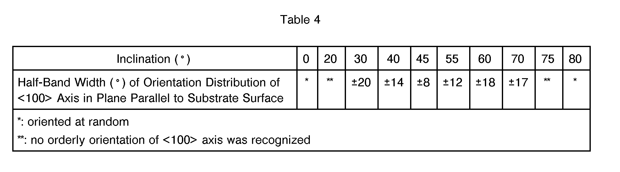
- An yttrium oxide superconducting thin film was formed on a small piece of a hastelloy tape which was previously provided with an amorphous yttria stabilized zirconia (YSZ) layer by laser ablation employing a KrF excimer laser of 248 nm in wavelength. First, the substrate and the target were arranged in parallel with each other as shown in Fig. 1 (a) to form the yttrium-based oxide superconducting thin film under conditions of a substrate temperature of 600 °C and an oxygen gas pressure of 200 mTorr, whereby it was confirmed that a <103> or <013> axis was most strongly oriented perpendicularly to the base material surface. In laser ablation, the laser was prepared from a KrF excimer laser of 248 nm in wavelength, while the target was prepared from a Y-based sintered body expressed as Y1Ba2Cu3Ox. Then, a small tape piece was inclined at an angle of 45° as shown in Fig. 1 (b), to form an yttrium-based oxide superconducting film under the same conditions as the above. This film exhibited the orientation of a <001> axis in a direction substantially perpendicular to the base material surface, while the same exhibited no orientation of a <103> or <013> axis. It was clarified through investigation by an X-ray pole figure technique that a <100> or <010> axis was strongly oriented in a direction parallel to the base material surface. Table 4 shows relations between inclinations and orientation distributions of the <100> axes in the base material surfaces. It was possible to obtain yttrium-based oxide superconducting films having strong single-crystallinity at inclinations in the range of 30 ° to 70 °.
- Cerium oxide and magnesium oxide were deposited under various substrate temperatures and oxygen gas pressures, similarly to Example 1. Consequently, it was confirmed that <100> axes were oriented perpendicularly to the substrate surfaces under conditions of 350 ° to 550 ° and 5 mTorr to 50 mTorr, and 400 °C to 600 °C and 50 mTorr to 100 mTorr respectively. The substrates were inclined at various angles, to form thin films of cerium oxide and magnesium oxide respectively under these conditions. Consequently, it was possible to obtain films strongly orienting <110> axes in planes parallel to the substrates when the inclinations were in the range of 30 ° to 70 °.
- Relations between the distributions of the <110> axes oriented in the planes parallel to the substrates and the inclinations were investigated by an X-ray pole figure technique. Table 5 shows the results.

- A small tape piece was inclined at 55 ° to form a YSZ thin film in the method of Example 1. A thin film of an yttrium-based oxide superconductor was formed on the YSZ film by laser ablation in substantially parallel arrangement of a substrate and a target. At this time, the substrate temperature and the oxygen gas pressure were set at 750 °C and 300 mTorr respectively. The YSZ thin film regularized its orientations with a half-band width of an in-plane <100> axis of ±7 similarly to Example 1, and the thin film of the yttrium-based oxide superconductor formed thereon oriented a c-axis perpendicularly to the substrate surface while orienting an a-axis at a half-band width of ±6 as the orientation distribution in a plane parallel to the substrate. Thus, it can be inferred that the yttrium-based superconducting film, which was a second film, was epitaxially grown with respect to the first film. This film exhibited a critical current density of 3.2 x 10⁵ A/cm2 in liquid nitrogen.
- A small tape piece was inclined at 45 ° to form a YSZ thin film in the method of Example 3. A thin film of an yttrium-based oxide superconductor was formed thereon by laser ablation, in substantially parallel arrangement of a substrate and a target. Forming conditions were identical to those in Example 6. The YSZ thin film regularized its orientations at a half-band width of ±7° of an in-plane <100> axis similarly to Example 3, and the thin film of the yttrium-based oxide superconductor formed thereon oriented a c-axis perpendicularly to the substrate surface while orienting an a-axis at a half-band width of ±5 ° as the orientation distribution in the plane. Thus, it can be inferred that the first and second films were in an epitaxial relation to each other, similarly to Example 6. This film exhibited a critical current density of 4.3 x 10⁵ A/cm2 in liquid nitrogen.
- According to the present invention, as hereinabove described, it is possible to form a single-crystalline thin film on a polycrystalline or amorphous base material through a simple process with the minimum equipment required for laser deposition. When the base material is prepared from a long metal tape, it is possible to form a single-crystalline thin film consisting essentially of yttria stabilized zirconia, magnesium oxide or cerium oxide thereon along the longitudinal direction of the tape. When an oxide superconductor is heteroepitaxially grown on this thin film, it is possible to form a superconductor exhibiting a high critical current density. It is also possible to form a superconductor having high single-crystallinity and exhibiting a high critical current density by applying the present invention to formation of an oxide superconducting film itself. When the superconductor is formed along the longitudinal direction of the tape, it is possible to obtain a superconducting wire. The present invention is particularly useful for a process of manufacturing an oxide superconducting wire.
- Although the present invention has been described and illustrated in detail, it is clearly understood that the same is by way of illustration and example only and is not to be taken by way of limitation, the spirit and scope of the present invention being limited only by the terms of the appended claims.
Claims (16)
and
Applications Claiming Priority (6)
| Application Number | Priority Date | Filing Date | Title |
|---|---|---|---|
| JP2802294 | 1994-02-25 | ||
| JP2802294 | 1994-02-25 | ||
| JP28022/94 | 1994-02-25 | ||
| JP26877694 | 1994-11-01 | ||
| JP26877694A JP3623001B2 (en) | 1994-02-25 | 1994-11-01 | Method for forming single crystalline thin film |
| JP268776/94 | 1994-11-01 |
Publications (3)
| Publication Number | Publication Date |
|---|---|
| EP0669411A2 true EP0669411A2 (en) | 1995-08-30 |
| EP0669411A3 EP0669411A3 (en) | 1997-11-19 |
| EP0669411B1 EP0669411B1 (en) | 1999-09-01 |
Family
ID=26366046
Family Applications (1)
| Application Number | Title | Priority Date | Filing Date |
|---|---|---|---|
| EP95102682A Expired - Lifetime EP0669411B1 (en) | 1994-02-25 | 1995-02-24 | Method of forming single-crystalline thin film |
Country Status (5)
| Country | Link |
|---|---|
| US (1) | US5607899A (en) |
| EP (1) | EP0669411B1 (en) |
| JP (1) | JP3623001B2 (en) |
| CA (1) | CA2143265C (en) |
| DE (1) | DE69511743T2 (en) |
Cited By (7)
| Publication number | Priority date | Publication date | Assignee | Title |
|---|---|---|---|---|
| WO1999025908A1 (en) * | 1997-11-13 | 1999-05-27 | The Board Of Trustees Of The Leland Stanford Junior University | Thin films having a rock-salt-like structure deposited on amorphous surfaces |
| WO2001059186A1 (en) * | 2000-02-09 | 2001-08-16 | Microcoating Technologies, Inc. | Processing line having means to monitor crystallographic orientation |
| WO2002072909A1 (en) * | 2001-03-09 | 2002-09-19 | Sumitomo Electric Industries, Ltd. | Laminated film and method of forming film |
| DE10248025A1 (en) * | 2002-10-15 | 2004-05-13 | THEVA DüNNSCHICHTTECHNIK GMBH | Layer material and method for improving the current carrying capacity of high-temperature superconductor thin layers |
| WO2012013415A1 (en) | 2010-07-29 | 2012-02-02 | THEVA DüNNSCHICHTTECHNIK GMBH | High temperature superconducting tape conductor having high critical ampacity |
| EP2991126A1 (en) | 2014-08-25 | 2016-03-02 | Theva Dünnschichttechnik GmbH | Method and device for producing a high temperature superconductor |
| EP3282493A1 (en) | 2016-08-10 | 2018-02-14 | Theva Dünnschichttechnik GmbH | High temperature superconductor tape having stainless steel substrate |
Families Citing this family (106)
| Publication number | Priority date | Publication date | Assignee | Title |
|---|---|---|---|---|
| JP2894279B2 (en) * | 1996-06-10 | 1999-05-24 | 日本電気株式会社 | Metal thin film forming method |
| JP4131771B2 (en) * | 1999-10-18 | 2008-08-13 | 株式会社フジクラ | Polycrystalline thin film, manufacturing method thereof and oxide superconducting conductor |
| US6509070B1 (en) * | 2000-09-22 | 2003-01-21 | The United States Of America As Represented By The Secretary Of The Air Force | Laser ablation, low temperature-fabricated yttria-stabilized zirconia oriented films |
| JP2003055095A (en) * | 2001-08-07 | 2003-02-26 | Sumitomo Electric Ind Ltd | Thin film formation method |
| JP4155796B2 (en) * | 2002-10-31 | 2008-09-24 | 住友電気工業株式会社 | Monocrystalline thin film |
| JP4155795B2 (en) * | 2002-10-31 | 2008-09-24 | 住友電気工業株式会社 | Method for forming oxide high-temperature superconductor thin film on substrate via intermediate layer |
| WO2010065163A2 (en) * | 2008-06-05 | 2010-06-10 | Soraa, Inc. | Highly polarized white light source by combining blue led on semipolar or nonpolar gan with yellow led on semipolar or nonpolar gan |
| US8847249B2 (en) * | 2008-06-16 | 2014-09-30 | Soraa, Inc. | Solid-state optical device having enhanced indium content in active regions |
| US8805134B1 (en) | 2012-02-17 | 2014-08-12 | Soraa Laser Diode, Inc. | Methods and apparatus for photonic integration in non-polar and semi-polar oriented wave-guided optical devices |
| US8143148B1 (en) | 2008-07-14 | 2012-03-27 | Soraa, Inc. | Self-aligned multi-dielectric-layer lift off process for laser diode stripes |
| US8259769B1 (en) | 2008-07-14 | 2012-09-04 | Soraa, Inc. | Integrated total internal reflectors for high-gain laser diodes with high quality cleaved facets on nonpolar/semipolar GaN substrates |
| US8284810B1 (en) | 2008-08-04 | 2012-10-09 | Soraa, Inc. | Solid state laser device using a selected crystal orientation in non-polar or semi-polar GaN containing materials and methods |
| US8124996B2 (en) | 2008-08-04 | 2012-02-28 | Soraa, Inc. | White light devices using non-polar or semipolar gallium containing materials and phosphors |
| US8242375B2 (en) * | 2008-09-18 | 2012-08-14 | United Technologies Corporation | Conductive emissions protection |
| US20100295088A1 (en) * | 2008-10-02 | 2010-11-25 | Soraa, Inc. | Textured-surface light emitting diode and method of manufacture |
| US8247886B1 (en) | 2009-03-09 | 2012-08-21 | Soraa, Inc. | Polarization direction of optical devices using selected spatial configurations |
| US8422525B1 (en) | 2009-03-28 | 2013-04-16 | Soraa, Inc. | Optical device structure using miscut GaN substrates for laser applications |
| US8634442B1 (en) | 2009-04-13 | 2014-01-21 | Soraa Laser Diode, Inc. | Optical device structure using GaN substrates for laser applications |
| US8294179B1 (en) | 2009-04-17 | 2012-10-23 | Soraa, Inc. | Optical device structure using GaN substrates and growth structures for laser applications |
| US8837545B2 (en) | 2009-04-13 | 2014-09-16 | Soraa Laser Diode, Inc. | Optical device structure using GaN substrates and growth structures for laser applications |
| DE112010001615T5 (en) | 2009-04-13 | 2012-08-02 | Soraa, Inc. | Structure of an optical element using GaN substrates for laser applications |
| US8242522B1 (en) | 2009-05-12 | 2012-08-14 | Soraa, Inc. | Optical device structure using non-polar GaN substrates and growth structures for laser applications in 481 nm |
| US8254425B1 (en) | 2009-04-17 | 2012-08-28 | Soraa, Inc. | Optical device structure using GaN substrates and growth structures for laser applications |
| US8416825B1 (en) | 2009-04-17 | 2013-04-09 | Soraa, Inc. | Optical device structure using GaN substrates and growth structure for laser applications |
| US8791499B1 (en) | 2009-05-27 | 2014-07-29 | Soraa, Inc. | GaN containing optical devices and method with ESD stability |
| US10108079B2 (en) | 2009-05-29 | 2018-10-23 | Soraa Laser Diode, Inc. | Laser light source for a vehicle |
| US9800017B1 (en) | 2009-05-29 | 2017-10-24 | Soraa Laser Diode, Inc. | Laser device and method for a vehicle |
| US8427590B2 (en) | 2009-05-29 | 2013-04-23 | Soraa, Inc. | Laser based display method and system |
| US9250044B1 (en) | 2009-05-29 | 2016-02-02 | Soraa Laser Diode, Inc. | Gallium and nitrogen containing laser diode dazzling devices and methods of use |
| US8509275B1 (en) | 2009-05-29 | 2013-08-13 | Soraa, Inc. | Gallium nitride based laser dazzling device and method |
| US8247887B1 (en) * | 2009-05-29 | 2012-08-21 | Soraa, Inc. | Method and surface morphology of non-polar gallium nitride containing substrates |
| US9829780B2 (en) | 2009-05-29 | 2017-11-28 | Soraa Laser Diode, Inc. | Laser light source for a vehicle |
| US20110056429A1 (en) * | 2009-08-21 | 2011-03-10 | Soraa, Inc. | Rapid Growth Method and Structures for Gallium and Nitrogen Containing Ultra-Thin Epitaxial Structures for Devices |
| US9000466B1 (en) | 2010-08-23 | 2015-04-07 | Soraa, Inc. | Methods and devices for light extraction from a group III-nitride volumetric LED using surface and sidewall roughening |
| US8314429B1 (en) | 2009-09-14 | 2012-11-20 | Soraa, Inc. | Multi color active regions for white light emitting diode |
| US8355418B2 (en) * | 2009-09-17 | 2013-01-15 | Soraa, Inc. | Growth structures and method for forming laser diodes on {20-21} or off cut gallium and nitrogen containing substrates |
| US8750342B1 (en) | 2011-09-09 | 2014-06-10 | Soraa Laser Diode, Inc. | Laser diodes with scribe structures |
| US8933644B2 (en) | 2009-09-18 | 2015-01-13 | Soraa, Inc. | LED lamps with improved quality of light |
| CN107256915A (en) | 2009-09-18 | 2017-10-17 | 天空公司 | LED device |
| US9583678B2 (en) | 2009-09-18 | 2017-02-28 | Soraa, Inc. | High-performance LED fabrication |
| US9293644B2 (en) | 2009-09-18 | 2016-03-22 | Soraa, Inc. | Power light emitting diode and method with uniform current density operation |
| US8905588B2 (en) | 2010-02-03 | 2014-12-09 | Sorra, Inc. | System and method for providing color light sources in proximity to predetermined wavelength conversion structures |
| US20110186874A1 (en) * | 2010-02-03 | 2011-08-04 | Soraa, Inc. | White Light Apparatus and Method |
| US10147850B1 (en) | 2010-02-03 | 2018-12-04 | Soraa, Inc. | System and method for providing color light sources in proximity to predetermined wavelength conversion structures |
| US20110182056A1 (en) * | 2010-06-23 | 2011-07-28 | Soraa, Inc. | Quantum Dot Wavelength Conversion for Optical Devices Using Nonpolar or Semipolar Gallium Containing Materials |
| US9927611B2 (en) | 2010-03-29 | 2018-03-27 | Soraa Laser Diode, Inc. | Wearable laser based display method and system |
| US8451876B1 (en) | 2010-05-17 | 2013-05-28 | Soraa, Inc. | Method and system for providing bidirectional light sources with broad spectrum |
| US9450143B2 (en) | 2010-06-18 | 2016-09-20 | Soraa, Inc. | Gallium and nitrogen containing triangular or diamond-shaped configuration for optical devices |
| US8816319B1 (en) | 2010-11-05 | 2014-08-26 | Soraa Laser Diode, Inc. | Method of strain engineering and related optical device using a gallium and nitrogen containing active region |
| US9048170B2 (en) | 2010-11-09 | 2015-06-02 | Soraa Laser Diode, Inc. | Method of fabricating optical devices using laser treatment |
| US8975615B2 (en) | 2010-11-09 | 2015-03-10 | Soraa Laser Diode, Inc. | Method of fabricating optical devices using laser treatment of contact regions of gallium and nitrogen containing material |
| US8786053B2 (en) | 2011-01-24 | 2014-07-22 | Soraa, Inc. | Gallium-nitride-on-handle substrate materials and devices and method of manufacture |
| US9025635B2 (en) | 2011-01-24 | 2015-05-05 | Soraa Laser Diode, Inc. | Laser package having multiple emitters configured on a support member |
| US9595813B2 (en) | 2011-01-24 | 2017-03-14 | Soraa Laser Diode, Inc. | Laser package having multiple emitters configured on a substrate member |
| US9318875B1 (en) | 2011-01-24 | 2016-04-19 | Soraa Laser Diode, Inc. | Color converting element for laser diode |
| US9093820B1 (en) | 2011-01-25 | 2015-07-28 | Soraa Laser Diode, Inc. | Method and structure for laser devices using optical blocking regions |
| US9287684B2 (en) | 2011-04-04 | 2016-03-15 | Soraa Laser Diode, Inc. | Laser package having multiple emitters with color wheel |
| US8686431B2 (en) | 2011-08-22 | 2014-04-01 | Soraa, Inc. | Gallium and nitrogen containing trilateral configuration for optical devices |
| US8971370B1 (en) | 2011-10-13 | 2015-03-03 | Soraa Laser Diode, Inc. | Laser devices using a semipolar plane |
| US8912025B2 (en) | 2011-11-23 | 2014-12-16 | Soraa, Inc. | Method for manufacture of bright GaN LEDs using a selective removal process |
| EP2823515A4 (en) | 2012-03-06 | 2015-08-19 | Soraa Inc | LIGHT EMITTING DIODE WITH LOW REFRACTIVE INDEX TO REDUCE LIGHT GUIDING EFFECTS |
| US9020003B1 (en) | 2012-03-14 | 2015-04-28 | Soraa Laser Diode, Inc. | Group III-nitride laser diode grown on a semi-polar orientation of gallium and nitrogen containing substrates |
| US9343871B1 (en) | 2012-04-05 | 2016-05-17 | Soraa Laser Diode, Inc. | Facet on a gallium and nitrogen containing laser diode |
| US9800016B1 (en) | 2012-04-05 | 2017-10-24 | Soraa Laser Diode, Inc. | Facet on a gallium and nitrogen containing laser diode |
| US10559939B1 (en) | 2012-04-05 | 2020-02-11 | Soraa Laser Diode, Inc. | Facet on a gallium and nitrogen containing laser diode |
| US9088135B1 (en) | 2012-06-29 | 2015-07-21 | Soraa Laser Diode, Inc. | Narrow sized laser diode |
| US9184563B1 (en) | 2012-08-30 | 2015-11-10 | Soraa Laser Diode, Inc. | Laser diodes with an etched facet and surface treatment |
| US9012848B2 (en) | 2012-10-02 | 2015-04-21 | Coherent, Inc. | Laser power and energy sensor utilizing anisotropic thermoelectric material |
| US9059346B2 (en) | 2012-10-02 | 2015-06-16 | Coherent, Inc. | Laser power and energy sensor utilizing anisotropic thermoelectric material |
| US9978904B2 (en) | 2012-10-16 | 2018-05-22 | Soraa, Inc. | Indium gallium nitride light emitting devices |
| US8802471B1 (en) | 2012-12-21 | 2014-08-12 | Soraa, Inc. | Contacts for an n-type gallium and nitrogen substrate for optical devices |
| US9166372B1 (en) | 2013-06-28 | 2015-10-20 | Soraa Laser Diode, Inc. | Gallium nitride containing laser device configured on a patterned substrate |
| US8994033B2 (en) | 2013-07-09 | 2015-03-31 | Soraa, Inc. | Contacts for an n-type gallium and nitrogen substrate for optical devices |
| JP6255647B2 (en) | 2013-07-25 | 2018-01-10 | 株式会社ユーテック | Crystal film, crystal film manufacturing method, vapor deposition apparatus, and multi-chamber apparatus |
| US9368939B2 (en) | 2013-10-18 | 2016-06-14 | Soraa Laser Diode, Inc. | Manufacturable laser diode formed on C-plane gallium and nitrogen material |
| US9520695B2 (en) | 2013-10-18 | 2016-12-13 | Soraa Laser Diode, Inc. | Gallium and nitrogen containing laser device having confinement region |
| US9362715B2 (en) | 2014-02-10 | 2016-06-07 | Soraa Laser Diode, Inc | Method for manufacturing gallium and nitrogen bearing laser devices with improved usage of substrate material |
| US9379525B2 (en) | 2014-02-10 | 2016-06-28 | Soraa Laser Diode, Inc. | Manufacturable laser diode |
| US9419189B1 (en) | 2013-11-04 | 2016-08-16 | Soraa, Inc. | Small LED source with high brightness and high efficiency |
| US9209596B1 (en) | 2014-02-07 | 2015-12-08 | Soraa Laser Diode, Inc. | Manufacturing a laser diode device from a plurality of gallium and nitrogen containing substrates |
| US9871350B2 (en) | 2014-02-10 | 2018-01-16 | Soraa Laser Diode, Inc. | Manufacturable RGB laser diode source |
| US9520697B2 (en) | 2014-02-10 | 2016-12-13 | Soraa Laser Diode, Inc. | Manufacturable multi-emitter laser diode |
| US9564736B1 (en) * | 2014-06-26 | 2017-02-07 | Soraa Laser Diode, Inc. | Epitaxial growth of p-type cladding regions using nitrogen gas for a gallium and nitrogen containing laser diode |
| US12126143B2 (en) | 2014-11-06 | 2024-10-22 | Kyocera Sld Laser, Inc. | Method of manufacture for an ultraviolet emitting optoelectronic device |
| US9246311B1 (en) | 2014-11-06 | 2016-01-26 | Soraa Laser Diode, Inc. | Method of manufacture for an ultraviolet laser diode |
| US9653642B1 (en) | 2014-12-23 | 2017-05-16 | Soraa Laser Diode, Inc. | Manufacturable RGB display based on thin film gallium and nitrogen containing light emitting diodes |
| US9666677B1 (en) | 2014-12-23 | 2017-05-30 | Soraa Laser Diode, Inc. | Manufacturable thin film gallium and nitrogen containing devices |
| US10879673B2 (en) | 2015-08-19 | 2020-12-29 | Soraa Laser Diode, Inc. | Integrated white light source using a laser diode and a phosphor in a surface mount device package |
| US10938182B2 (en) | 2015-08-19 | 2021-03-02 | Soraa Laser Diode, Inc. | Specialized integrated light source using a laser diode |
| US11437775B2 (en) | 2015-08-19 | 2022-09-06 | Kyocera Sld Laser, Inc. | Integrated light source using a laser diode |
| US11437774B2 (en) | 2015-08-19 | 2022-09-06 | Kyocera Sld Laser, Inc. | High-luminous flux laser-based white light source |
| US9787963B2 (en) | 2015-10-08 | 2017-10-10 | Soraa Laser Diode, Inc. | Laser lighting having selective resolution |
| US10995624B2 (en) * | 2016-08-01 | 2021-05-04 | General Electric Company | Article for high temperature service |
| US10771155B2 (en) | 2017-09-28 | 2020-09-08 | Soraa Laser Diode, Inc. | Intelligent visible light with a gallium and nitrogen containing laser source |
| US10222474B1 (en) | 2017-12-13 | 2019-03-05 | Soraa Laser Diode, Inc. | Lidar systems including a gallium and nitrogen containing laser light source |
| US10551728B1 (en) | 2018-04-10 | 2020-02-04 | Soraa Laser Diode, Inc. | Structured phosphors for dynamic lighting |
| US11239637B2 (en) | 2018-12-21 | 2022-02-01 | Kyocera Sld Laser, Inc. | Fiber delivered laser induced white light system |
| US11421843B2 (en) | 2018-12-21 | 2022-08-23 | Kyocera Sld Laser, Inc. | Fiber-delivered laser-induced dynamic light system |
| US11884202B2 (en) | 2019-01-18 | 2024-01-30 | Kyocera Sld Laser, Inc. | Laser-based fiber-coupled white light system |
| US12152742B2 (en) | 2019-01-18 | 2024-11-26 | Kyocera Sld Laser, Inc. | Laser-based light guide-coupled wide-spectrum light system |
| US12000552B2 (en) | 2019-01-18 | 2024-06-04 | Kyocera Sld Laser, Inc. | Laser-based fiber-coupled white light system for a vehicle |
| US11228158B2 (en) | 2019-05-14 | 2022-01-18 | Kyocera Sld Laser, Inc. | Manufacturable laser diodes on a large area gallium and nitrogen containing substrate |
| US10903623B2 (en) | 2019-05-14 | 2021-01-26 | Soraa Laser Diode, Inc. | Method and structure for manufacturable large area gallium and nitrogen containing substrate |
| TWI743525B (en) | 2019-07-30 | 2021-10-21 | 國立陽明交通大學 | Quasi-single-crystal film and manufacturing method thereof |
| TWI726777B (en) | 2020-07-27 | 2021-05-01 | 國立陽明交通大學 | Large grain quasi-single-crystal film and manufacturing method thereof |
| US12191626B1 (en) | 2020-07-31 | 2025-01-07 | Kyocera Sld Laser, Inc. | Vertically emitting laser devices and chip-scale-package laser devices and laser-based, white light emitting devices |
Family Cites Families (11)
| Publication number | Priority date | Publication date | Assignee | Title |
|---|---|---|---|---|
| US5077270A (en) * | 1987-03-26 | 1991-12-31 | Matsushita Electric Industrial Co., Ltd. | Elements comprising a film of a perovskite compound whose crystallographic axes are oriented and a method of making such elements |
| JP2650910B2 (en) * | 1987-04-22 | 1997-09-10 | 株式会社日立製作所 | Method of forming oxide superconductor thin film |
| EP0343649A1 (en) * | 1988-05-24 | 1989-11-29 | Siemens Aktiengesellschaft | Method of making thin films of superconducting material and films made therewith |
| JPH0826451B2 (en) * | 1989-04-13 | 1996-03-13 | 松下電器産業株式会社 | Sputtering method |
| JP2822447B2 (en) * | 1989-05-19 | 1998-11-11 | 住友電気工業株式会社 | Method and apparatus for producing oxide superconducting wire |
| JPH03174307A (en) * | 1989-11-30 | 1991-07-29 | Chiyoudendou Hatsuden Kanren Kiki Zairyo Gijutsu Kenkyu Kumiai | Production of oxide superconductor |
| JPH03188272A (en) * | 1989-12-14 | 1991-08-16 | Matsushita Electric Ind Co Ltd | Laser sputtering device |
| JPH0446082A (en) * | 1990-06-13 | 1992-02-17 | Sumitomo Electric Ind Ltd | Formation of high-quality oxide superconducting thin film |
| US5597411A (en) * | 1991-02-19 | 1997-01-28 | Energy Conversion Devices, Inc. | Method of forming a single crystal material |
| US5242706A (en) * | 1991-07-31 | 1993-09-07 | The United States Of America As Represented By The Secretary Of The Navy | Laser-deposited biocompatible films and methods and apparatuses for producing same |
| DE69324633T2 (en) * | 1992-07-30 | 1999-12-16 | Sumitomo Electric Industries, Ltd. | Process for producing a single-crystal thin film |
-
1994
- 1994-11-01 JP JP26877694A patent/JP3623001B2/en not_active Expired - Fee Related
-
1995
- 1995-02-23 CA CA002143265A patent/CA2143265C/en not_active Expired - Fee Related
- 1995-02-24 EP EP95102682A patent/EP0669411B1/en not_active Expired - Lifetime
- 1995-02-24 DE DE69511743T patent/DE69511743T2/en not_active Expired - Lifetime
- 1995-02-24 US US08/393,747 patent/US5607899A/en not_active Expired - Lifetime
Cited By (12)
| Publication number | Priority date | Publication date | Assignee | Title |
|---|---|---|---|---|
| WO1999025908A1 (en) * | 1997-11-13 | 1999-05-27 | The Board Of Trustees Of The Leland Stanford Junior University | Thin films having a rock-salt-like structure deposited on amorphous surfaces |
| US6190752B1 (en) | 1997-11-13 | 2001-02-20 | Board Of Trustees Of The Leland Stanford Junior University | Thin films having rock-salt-like structure deposited on amorphous surfaces |
| WO2001059186A1 (en) * | 2000-02-09 | 2001-08-16 | Microcoating Technologies, Inc. | Processing line having means to monitor crystallographic orientation |
| WO2002072909A1 (en) * | 2001-03-09 | 2002-09-19 | Sumitomo Electric Industries, Ltd. | Laminated film and method of forming film |
| AU2002221113B2 (en) * | 2001-03-09 | 2007-03-29 | Sumitomo Electric Industries, Ltd. | Laminated film and method of forming film |
| EP1375697A4 (en) * | 2001-03-09 | 2008-08-27 | Sumitomo Electric Industries | Laminated film and method of forming film |
| US7544273B2 (en) | 2001-03-09 | 2009-06-09 | Sumitomo Electric Industries, Ltd. | Deposition methods and stacked film formed thereby |
| DE10248025A1 (en) * | 2002-10-15 | 2004-05-13 | THEVA DüNNSCHICHTTECHNIK GMBH | Layer material and method for improving the current carrying capacity of high-temperature superconductor thin layers |
| WO2012013415A1 (en) | 2010-07-29 | 2012-02-02 | THEVA DüNNSCHICHTTECHNIK GMBH | High temperature superconducting tape conductor having high critical ampacity |
| DE102010038656A1 (en) | 2010-07-29 | 2012-02-02 | THEVA DüNNSCHICHTTECHNIK GMBH | High-temperature superconductor strip conductor with high critical current carrying capacity |
| EP2991126A1 (en) | 2014-08-25 | 2016-03-02 | Theva Dünnschichttechnik GmbH | Method and device for producing a high temperature superconductor |
| EP3282493A1 (en) | 2016-08-10 | 2018-02-14 | Theva Dünnschichttechnik GmbH | High temperature superconductor tape having stainless steel substrate |
Also Published As
| Publication number | Publication date |
|---|---|
| CA2143265A1 (en) | 1995-08-26 |
| DE69511743D1 (en) | 1999-10-07 |
| JPH07291626A (en) | 1995-11-07 |
| CA2143265C (en) | 1998-10-06 |
| EP0669411B1 (en) | 1999-09-01 |
| US5607899A (en) | 1997-03-04 |
| DE69511743T2 (en) | 2000-04-27 |
| JP3623001B2 (en) | 2005-02-23 |
| EP0669411A3 (en) | 1997-11-19 |
Similar Documents
| Publication | Publication Date | Title |
|---|---|---|
| US5607899A (en) | Method of forming single-crystalline thin film | |
| EP0581254B1 (en) | Method of forming single-crystalline thin film | |
| US6921741B2 (en) | Substrate structure for growth of highly oriented and/or epitaxial layers thereon | |
| US8216978B2 (en) | Fluorinated precursors of superconducting ceramics, and methods of making the same | |
| US7736761B2 (en) | Buffer layer for thin film structures | |
| US7258927B2 (en) | High rate buffer layer for IBAD MgO coated conductors | |
| US6466805B2 (en) | Shielded high-Tc bscco tapes or wires for high field applications | |
| US7727934B2 (en) | Architecture for coated conductors | |
| US5212151A (en) | Superconducting thin film having a matrix and foreign phases | |
| Wang et al. | Film microstructure-deposition condition relationships in the growth of epitaxial NiO films by metalorganic chemical vapor deposition on oxide and metal substrates | |
| US5130296A (en) | Method of preparing an oxide superconducting thin film on a substrate with a plurality of grooves | |
| CA2031591C (en) | Oxide superconducting thin film | |
| Wells et al. | In-plane aligned YBCO thick films on {110} rolled and single crystal silver by ultrasonic mist pyrolysis | |
| JP3045705B2 (en) | Oxide-based superconducting material, method for producing the same, and apparatus using the same | |
| Varlashkin et al. | Universal texturing layer for high-current HTSC tapes | |
| Reddy et al. | A novel process for textured thick film YBa2Cu3O y coated conductors based on a constitutional gradients principle | |
| Asano et al. | Epitaxial growth of superconducting Nb3Ge films on YSZ single-crystal substrates | |
| Mozhaev et al. | Tilted-axes YBCO thin films: from vicinal range to step bunching | |
| JPH01167912A (en) | Sheathing material of superconducting material and manufacture thereof | |
| JPH08109469A (en) | Method for producing metal oxide thin film | |
| JPH0692787A (en) | Method for forming single crystalline thin film | |
| JP2004207482A (en) | Oxide superconductive thin film | |
| Norton et al. | Epitaxial growth of oxide thin films on (001) metal surfaces using pulsed-laser deposition | |
| Burger et al. | Scanning Tunneling Microscopy of Surface Properties of Epitaxial YBa sub 2 Cu sub 3 O sub md delta and Bi sub 2 Sr sub 2 Ca sub 1 Cu sub 2 O sub 8+ delta High-T sub c Thin Films Prepared by Different Methods | |
| Chang et al. | Substrate Effects on The Growth of Oriented MgO Thin Films |
Legal Events
| Date | Code | Title | Description |
|---|---|---|---|
| PUAI | Public reference made under article 153(3) epc to a published international application that has entered the european phase |
Free format text: ORIGINAL CODE: 0009012 |
|
| AK | Designated contracting states |
Kind code of ref document: A2 Designated state(s): DE FR GB |
|
| PUAL | Search report despatched |
Free format text: ORIGINAL CODE: 0009013 |
|
| AK | Designated contracting states |
Kind code of ref document: A3 Designated state(s): DE FR GB |
|
| 17P | Request for examination filed |
Effective date: 19971118 |
|
| 17Q | First examination report despatched |
Effective date: 19980113 |
|
| GRAG | Despatch of communication of intention to grant |
Free format text: ORIGINAL CODE: EPIDOS AGRA |
|
| GRAG | Despatch of communication of intention to grant |
Free format text: ORIGINAL CODE: EPIDOS AGRA |
|
| GRAG | Despatch of communication of intention to grant |
Free format text: ORIGINAL CODE: EPIDOS AGRA |
|
| GRAH | Despatch of communication of intention to grant a patent |
Free format text: ORIGINAL CODE: EPIDOS IGRA |
|
| GRAH | Despatch of communication of intention to grant a patent |
Free format text: ORIGINAL CODE: EPIDOS IGRA |
|
| GRAA | (expected) grant |
Free format text: ORIGINAL CODE: 0009210 |
|
| AK | Designated contracting states |
Kind code of ref document: B1 Designated state(s): DE FR GB |
|
| REF | Corresponds to: |
Ref document number: 69511743 Country of ref document: DE Date of ref document: 19991007 |
|
| ET | Fr: translation filed | ||
| PLBE | No opposition filed within time limit |
Free format text: ORIGINAL CODE: 0009261 |
|
| STAA | Information on the status of an ep patent application or granted ep patent |
Free format text: STATUS: NO OPPOSITION FILED WITHIN TIME LIMIT |
|
| 26N | No opposition filed | ||
| REG | Reference to a national code |
Ref country code: GB Ref legal event code: IF02 |
|
| PGFP | Annual fee paid to national office [announced via postgrant information from national office to epo] |
Ref country code: FR Payment date: 20100223 Year of fee payment: 16 |
|
| PGFP | Annual fee paid to national office [announced via postgrant information from national office to epo] |
Ref country code: GB Payment date: 20100202 Year of fee payment: 16 Ref country code: DE Payment date: 20100303 Year of fee payment: 16 |
|
| GBPC | Gb: european patent ceased through non-payment of renewal fee |
Effective date: 20110224 |
|
| REG | Reference to a national code |
Ref country code: FR Ref legal event code: ST Effective date: 20111102 |
|
| REG | Reference to a national code |
Ref country code: DE Ref legal event code: R119 Ref document number: 69511743 Country of ref document: DE Effective date: 20110901 |
|
| PG25 | Lapsed in a contracting state [announced via postgrant information from national office to epo] |
Ref country code: FR Free format text: LAPSE BECAUSE OF NON-PAYMENT OF DUE FEES Effective date: 20110228 |
|
| PG25 | Lapsed in a contracting state [announced via postgrant information from national office to epo] |
Ref country code: GB Free format text: LAPSE BECAUSE OF NON-PAYMENT OF DUE FEES Effective date: 20110224 |
|
| PG25 | Lapsed in a contracting state [announced via postgrant information from national office to epo] |
Ref country code: DE Free format text: LAPSE BECAUSE OF NON-PAYMENT OF DUE FEES Effective date: 20110901 |