EP0674019A1 - Dispositifs semi-conducteurs et leurs procédés de fabrication - Google Patents
Dispositifs semi-conducteurs et leurs procédés de fabrication Download PDFInfo
- Publication number
- EP0674019A1 EP0674019A1 EP95103656A EP95103656A EP0674019A1 EP 0674019 A1 EP0674019 A1 EP 0674019A1 EP 95103656 A EP95103656 A EP 95103656A EP 95103656 A EP95103656 A EP 95103656A EP 0674019 A1 EP0674019 A1 EP 0674019A1
- Authority
- EP
- European Patent Office
- Prior art keywords
- alkoxide
- lead
- titanium
- zirconium
- forming
- Prior art date
- Legal status (The legal status is an assumption and is not a legal conclusion. Google has not performed a legal analysis and makes no representation as to the accuracy of the status listed.)
- Granted
Links
Images


Classifications
-
- C—CHEMISTRY; METALLURGY
- C23—COATING METALLIC MATERIAL; COATING MATERIAL WITH METALLIC MATERIAL; CHEMICAL SURFACE TREATMENT; DIFFUSION TREATMENT OF METALLIC MATERIAL; COATING BY VACUUM EVAPORATION, BY SPUTTERING, BY ION IMPLANTATION OR BY CHEMICAL VAPOUR DEPOSITION, IN GENERAL; INHIBITING CORROSION OF METALLIC MATERIAL OR INCRUSTATION IN GENERAL
- C23C—COATING METALLIC MATERIAL; COATING MATERIAL WITH METALLIC MATERIAL; SURFACE TREATMENT OF METALLIC MATERIAL BY DIFFUSION INTO THE SURFACE, BY CHEMICAL CONVERSION OR SUBSTITUTION; COATING BY VACUUM EVAPORATION, BY SPUTTERING, BY ION IMPLANTATION OR BY CHEMICAL VAPOUR DEPOSITION, IN GENERAL
- C23C18/00—Chemical coating by decomposition of either liquid compounds or solutions of the coating forming compounds, without leaving reaction products of surface material in the coating; Contact plating
- C23C18/02—Chemical coating by decomposition of either liquid compounds or solutions of the coating forming compounds, without leaving reaction products of surface material in the coating; Contact plating by thermal decomposition
- C23C18/12—Chemical coating by decomposition of either liquid compounds or solutions of the coating forming compounds, without leaving reaction products of surface material in the coating; Contact plating by thermal decomposition characterised by the deposition of inorganic material other than metallic material
- C23C18/1204—Chemical coating by decomposition of either liquid compounds or solutions of the coating forming compounds, without leaving reaction products of surface material in the coating; Contact plating by thermal decomposition characterised by the deposition of inorganic material other than metallic material inorganic material, e.g. non-oxide and non-metallic such as sulfides, nitrides based compounds
- C23C18/1208—Oxides, e.g. ceramics
- C23C18/1216—Metal oxides
-
- C—CHEMISTRY; METALLURGY
- C23—COATING METALLIC MATERIAL; COATING MATERIAL WITH METALLIC MATERIAL; CHEMICAL SURFACE TREATMENT; DIFFUSION TREATMENT OF METALLIC MATERIAL; COATING BY VACUUM EVAPORATION, BY SPUTTERING, BY ION IMPLANTATION OR BY CHEMICAL VAPOUR DEPOSITION, IN GENERAL; INHIBITING CORROSION OF METALLIC MATERIAL OR INCRUSTATION IN GENERAL
- C23C—COATING METALLIC MATERIAL; COATING MATERIAL WITH METALLIC MATERIAL; SURFACE TREATMENT OF METALLIC MATERIAL BY DIFFUSION INTO THE SURFACE, BY CHEMICAL CONVERSION OR SUBSTITUTION; COATING BY VACUUM EVAPORATION, BY SPUTTERING, BY ION IMPLANTATION OR BY CHEMICAL VAPOUR DEPOSITION, IN GENERAL
- C23C18/00—Chemical coating by decomposition of either liquid compounds or solutions of the coating forming compounds, without leaving reaction products of surface material in the coating; Contact plating
- C23C18/02—Chemical coating by decomposition of either liquid compounds or solutions of the coating forming compounds, without leaving reaction products of surface material in the coating; Contact plating by thermal decomposition
- C23C18/12—Chemical coating by decomposition of either liquid compounds or solutions of the coating forming compounds, without leaving reaction products of surface material in the coating; Contact plating by thermal decomposition characterised by the deposition of inorganic material other than metallic material
- C23C18/1225—Deposition of multilayers of inorganic material
-
- C—CHEMISTRY; METALLURGY
- C23—COATING METALLIC MATERIAL; COATING MATERIAL WITH METALLIC MATERIAL; CHEMICAL SURFACE TREATMENT; DIFFUSION TREATMENT OF METALLIC MATERIAL; COATING BY VACUUM EVAPORATION, BY SPUTTERING, BY ION IMPLANTATION OR BY CHEMICAL VAPOUR DEPOSITION, IN GENERAL; INHIBITING CORROSION OF METALLIC MATERIAL OR INCRUSTATION IN GENERAL
- C23C—COATING METALLIC MATERIAL; COATING MATERIAL WITH METALLIC MATERIAL; SURFACE TREATMENT OF METALLIC MATERIAL BY DIFFUSION INTO THE SURFACE, BY CHEMICAL CONVERSION OR SUBSTITUTION; COATING BY VACUUM EVAPORATION, BY SPUTTERING, BY ION IMPLANTATION OR BY CHEMICAL VAPOUR DEPOSITION, IN GENERAL
- C23C18/00—Chemical coating by decomposition of either liquid compounds or solutions of the coating forming compounds, without leaving reaction products of surface material in the coating; Contact plating
- C23C18/02—Chemical coating by decomposition of either liquid compounds or solutions of the coating forming compounds, without leaving reaction products of surface material in the coating; Contact plating by thermal decomposition
- C23C18/12—Chemical coating by decomposition of either liquid compounds or solutions of the coating forming compounds, without leaving reaction products of surface material in the coating; Contact plating by thermal decomposition characterised by the deposition of inorganic material other than metallic material
- C23C18/125—Process of deposition of the inorganic material
- C23C18/1254—Sol or sol-gel processing
-
- C—CHEMISTRY; METALLURGY
- C23—COATING METALLIC MATERIAL; COATING MATERIAL WITH METALLIC MATERIAL; CHEMICAL SURFACE TREATMENT; DIFFUSION TREATMENT OF METALLIC MATERIAL; COATING BY VACUUM EVAPORATION, BY SPUTTERING, BY ION IMPLANTATION OR BY CHEMICAL VAPOUR DEPOSITION, IN GENERAL; INHIBITING CORROSION OF METALLIC MATERIAL OR INCRUSTATION IN GENERAL
- C23C—COATING METALLIC MATERIAL; COATING MATERIAL WITH METALLIC MATERIAL; SURFACE TREATMENT OF METALLIC MATERIAL BY DIFFUSION INTO THE SURFACE, BY CHEMICAL CONVERSION OR SUBSTITUTION; COATING BY VACUUM EVAPORATION, BY SPUTTERING, BY ION IMPLANTATION OR BY CHEMICAL VAPOUR DEPOSITION, IN GENERAL
- C23C18/00—Chemical coating by decomposition of either liquid compounds or solutions of the coating forming compounds, without leaving reaction products of surface material in the coating; Contact plating
- C23C18/02—Chemical coating by decomposition of either liquid compounds or solutions of the coating forming compounds, without leaving reaction products of surface material in the coating; Contact plating by thermal decomposition
- C23C18/12—Chemical coating by decomposition of either liquid compounds or solutions of the coating forming compounds, without leaving reaction products of surface material in the coating; Contact plating by thermal decomposition characterised by the deposition of inorganic material other than metallic material
- C23C18/125—Process of deposition of the inorganic material
- C23C18/1279—Process of deposition of the inorganic material performed under reactive atmosphere, e.g. oxidising or reducing atmospheres
-
- C—CHEMISTRY; METALLURGY
- C23—COATING METALLIC MATERIAL; COATING MATERIAL WITH METALLIC MATERIAL; CHEMICAL SURFACE TREATMENT; DIFFUSION TREATMENT OF METALLIC MATERIAL; COATING BY VACUUM EVAPORATION, BY SPUTTERING, BY ION IMPLANTATION OR BY CHEMICAL VAPOUR DEPOSITION, IN GENERAL; INHIBITING CORROSION OF METALLIC MATERIAL OR INCRUSTATION IN GENERAL
- C23C—COATING METALLIC MATERIAL; COATING MATERIAL WITH METALLIC MATERIAL; SURFACE TREATMENT OF METALLIC MATERIAL BY DIFFUSION INTO THE SURFACE, BY CHEMICAL CONVERSION OR SUBSTITUTION; COATING BY VACUUM EVAPORATION, BY SPUTTERING, BY ION IMPLANTATION OR BY CHEMICAL VAPOUR DEPOSITION, IN GENERAL
- C23C18/00—Chemical coating by decomposition of either liquid compounds or solutions of the coating forming compounds, without leaving reaction products of surface material in the coating; Contact plating
- C23C18/02—Chemical coating by decomposition of either liquid compounds or solutions of the coating forming compounds, without leaving reaction products of surface material in the coating; Contact plating by thermal decomposition
- C23C18/12—Chemical coating by decomposition of either liquid compounds or solutions of the coating forming compounds, without leaving reaction products of surface material in the coating; Contact plating by thermal decomposition characterised by the deposition of inorganic material other than metallic material
- C23C18/125—Process of deposition of the inorganic material
- C23C18/1295—Process of deposition of the inorganic material with after-treatment of the deposited inorganic material
-
- H—ELECTRICITY
- H10—SEMICONDUCTOR DEVICES; ELECTRIC SOLID-STATE DEVICES NOT OTHERWISE PROVIDED FOR
- H10P—GENERIC PROCESSES OR APPARATUS FOR THE MANUFACTURE OR TREATMENT OF DEVICES COVERED BY CLASS H10
- H10P14/00—Formation of materials, e.g. in the shape of layers or pillars
- H10P14/60—Formation of materials, e.g. in the shape of layers or pillars of insulating materials
- H10P14/63—Formation of materials, e.g. in the shape of layers or pillars of insulating materials characterised by the formation processes
- H10P14/6326—Deposition processes
- H10P14/6342—Liquid deposition, e.g. spin-coating, sol-gel techniques or spray coating
-
- H—ELECTRICITY
- H10—SEMICONDUCTOR DEVICES; ELECTRIC SOLID-STATE DEVICES NOT OTHERWISE PROVIDED FOR
- H10P—GENERIC PROCESSES OR APPARATUS FOR THE MANUFACTURE OR TREATMENT OF DEVICES COVERED BY CLASS H10
- H10P14/00—Formation of materials, e.g. in the shape of layers or pillars
- H10P14/60—Formation of materials, e.g. in the shape of layers or pillars of insulating materials
- H10P14/69—Inorganic materials
- H10P14/692—Inorganic materials composed of oxides, glassy oxides or oxide-based glasses
- H10P14/6938—Inorganic materials composed of oxides, glassy oxides or oxide-based glasses the material containing at least one metal element, e.g. metal oxides, metal oxynitrides or metal oxycarbides
- H10P14/69398—Inorganic materials composed of oxides, glassy oxides or oxide-based glasses the material containing at least one metal element, e.g. metal oxides, metal oxynitrides or metal oxycarbides the material having a perovskite structure, e.g. BaTiO3
Definitions
- This invention is concerned with a method for forming a ferroelectric film (in particular, a lead zirconate titanate (PZT) film) by the sol gel method, a method to manufacture a capacitor (in particular, a capacitor in a semiconductor memory cell), a method to prepare its source solution, and the source solution.
- a ferroelectric film in particular, a lead zirconate titanate (PZT) film
- PZT lead zirconate titanate
- An ONO film that is structured to have successively laminated SiO2, Si3N4, and SiO2 is used as an insulating film (dielectric film) that makes up a capacitor for memory cells in a dynamic RAM, for example.
- the effective dielectric constant of said ONO film is small, at approximately 5, so the thickness of the capacitor dielectric film must be made thin under restrictions that concern the size of the area and complexity of shape that is required in order to expand the area when a large-capacity memory of less than 256 Mb is used, thus bringing much difficulty into the process.
- the sol gel method for forming a PZT film, referred to as Pb(Zr, Ti)O3, among the ferroelectric materials, the sol gel method, CVD (chemical vapor-phase growth) method, and the sputtering method, for example, can be used as the method for forming thin films. Formation by the sol gel method is particularly preferable. When forming films by the sol gel method, the quality of the source solution (sol gel solution) prepared determines the electrical characteristics of the thin film obtained at the end.
- the hydrate lead triacetate Pb(CH3COC)2 ⁇ 3H2O as the raw material is diluted with a solvent (methoxyethanol is often used in many cases, for example) in process 1.
- the water of crystallization of the hydrate lead triacetate is successively eliminated through boiling at 120-160°C in process 2.
- titanium ⁇ isopropoxide Ti ⁇ (CH3)2CHO ⁇ 4 and zirconium ⁇ n-butoxide Zr ⁇ (CH3(CH2)2CH2O ⁇ 4 are added to said lead acetate solution in process 3.
- Diethanolamine may be added at the same time as a stabilizer.
- This sol gel solution (source solution) is then coated on top of a substrate by the spin-coating method or the dip-coating method, for example, dried at a temperature of 100-300°C, with the thin-coated sol gel film being changed into a dried gel condition (polymer gel).
- a thin sintered film of Pb(Zr, Ti)O3 with a perovskite crystal structure -- the thin PZT film -- is formed from the dry gel through an oxidation sintering process in a high-temperature oxidizing atmosphere of above 600°C.
- each of the double alkoxides: PbTiO2 ⁇ OCH(CH3)2 ⁇ 2 and PbZrO2 ⁇ OCH2(CH2)2CH3 ⁇ 2 formed in process 4 has different alcohol residues (OR), so the hydrolysis and condensation in process 6 and process 7 do not uniformly advance, and different types of alcohol residues (OR) are mixed and present in the molecules formed in each of these reaction stages.
- Such different alcohol residues namely the isopropoxy group and the n-butoxy group, have a different reaction speed during hydrolysis and may react with other by-products in some cases. Therefore, it is highly possible that various types of molecular structures will be mixed and present in the condensation products formed, that structural separations will be caused, or various types of by-products will be formed.
- methoxyethanol used as the solvent also participates in the reaction in the manner below, so this solvent reacts with the alkoxide of process 3 during process 4 and mixes with the double alkoxide, further allowing the reaction to be nonuniform. This cannot be avoided even when the aforementioned alcohol residues (OR) are the same in both double alkoxides.
- the aim of this invention is to provide: a method for forming a ferroelectric film having excellent membranaceousness and electrical characteristics as a result of uniform reactions during the preparatory processes for the sol gel solution, along with a satisfactory acceleration in the polymerization of the metallic oxides. It also concerns a method for manufacturing a capacitor using said film, as well as a method for preparing the source solution (sol gel solution), and the source solution itself.
- This inventor has elucidated the complicated reactions occurring during the aforementioned preparatory processes for the sol gel solution, has clarified the polymerization processes of a precursor of the metallic oxide (double alkoxide) by reviewing the processing conditions of the preparatory processes, and has established new preparatory processes.
- this invention involves a process consisting of: a process (a) for obtaining fatty acid lead, a process (b) for obtaining titanium ⁇ alkoxide, a process (c) for obtaining zirconium ⁇ alkoxide that has the same alcohol residue as said titanium ⁇ alkoxide, and a process (d) for forming lead titanium ⁇ double alkoxide and lead zirconium ⁇ double alkoxide by mixing together the aforementioned fatty acid lead, the aforementioned titanium ⁇ alkoxide, and the aforementioned zirconium ⁇ alkoxide.
- the method for forming the ferroelectric film in this invention consists of: a process (a) for forming fatty acid lead (lead acetate Pb(CH3COO)2, for example) in which a hydrate fatty acid lead (hydrate lead acetate Pb(CH3COO)2 ⁇ 3H2O, for example) is first diluted by an alcohol solvent (methoxyethanol CH3OC2H4OH, for example) then boiled at 120-180°C, for example, for 30 min to 2 h in order to eliminate the water of crystallization, a process (b) for forming titanium ⁇ alkoxide (titanium ⁇ methoxyethoxide Ti(OC2H4OCH3)4, for example) through an alcohol exchange in which titanium ⁇ alkoxide (titanium ⁇ isopropoxide Ti ⁇ (CH3)2CHO ⁇ 4, for example) as the raw material is first diluted by the aforementioned alcohol solvent, then boiled at a temperature above the boiling point of the alcohol (isopropyl alcohol
- Precipitation of the products and formation of the by-products can be prevented by boiling the reaction solution at a temperature above 100°C after the polymerization of said reaction products.
- a stabilizer consisting of an alkanolamine (diethanolamine, for example) and/or ⁇ -diketone (acetylacetone, for example) may be added in order to prevent the precipitation of the products at least during the process for forming the titanium lead ⁇ double alkoxide and zirconium lead ⁇ double alkoxide from each of the aforementioned processes.
- the amount added is preferably less than 1.0 times that of the total number of moles of the constitutive metals of the ferroelectric film.
- Quaternary metallic elements such as lanthanum, niobium, and iron, for example, may be added during the forming process of the double alkoxide, for example, in the aforementioned processes in order to prevent fatigue (reduction in the remanence value) and a leakage of current through an inversion of the voltage applied when the formed thin PZT film is used.
- a ferroelectric film can be formed by coating this source, forming a dry film by drying this coated source solution, and sintering said dry film.
- This invention also provides a method for manufacturing a capacitor (capacitor in a semiconductor memory device, for example) in which the ferroelectric film is formed by coating the aforementioned prepared source solution on top of an upper electrode, drying it, and sintering the obtained dry film, with the unnecessary portion of this film being eliminated and the ferroelectric film being left in a specific pattern on top of the aforementioned upper electrode, and with an upper electrode being further formed on top of said ferroelectric film.
- This invention also provides a method to prepare a source solution for the ferroelectric film through each of the aforementioned processes, and also provides the prepared source solution itself.
- process I in which water of crystallization in the hydrate lead triacetate Pb(CH3COO)2 ⁇ 3H2O is eliminated; processes II and III in which titanium ⁇ isopropoxide Ti ⁇ (CH3)2CHO ⁇ 4 and zirconium ⁇ n-butoxide Zr ⁇ CH3(CH2)2CH2O ⁇ 4 are respectively provided with an alcohol exchange after being diluted with a solvent (methoxyethanol CH3OC2H4OH); process IV in which a double alkoxide is formed and the by-products are eliminated at the same time; and processes VII and VIII in which polymerization through hydrolysis and the condensation reaction are accelerated.
- process II and III in which titanium ⁇ isopropoxide Ti ⁇ (CH3)2CHO ⁇ 4 and zirconium ⁇ n-butoxide Zr ⁇ CH3(CH2)2CH2O ⁇ 4 are respectively provided with an alcohol exchange after being diluted with a solvent (methoxyethanol CH3OC2H4OH); process IV in which a double alkoxide is formed and the by-products are eliminated
- CH3OC2H4OH has a [-OH] (hydroxyl group) and performs an alcohol exchange between Zr(OR b )4 through boiling above the boiling point (117.4°C) of n-butanol R b OH, particularly 70-190°C (160°C, for example), for 30 min to 2 h (1 h, for example).
- the concentration of the double alkoxide increases according to the consumption or distillation of RmOH during the aforementioned process, so the solvent RmOH is added to dilute it to the desirable concentration.
- the aforementioned organometallic compound (double alkoxide) is formed as an intermediate product in the solution obtained through distillation during process IV, and the -ORm groups that are present in such material undergo hydrolysis when encountering H2O, as indicated below, and are changed into [-OH] groups.
- -OH condenses with other -OH, and the H2O formed here again contributes to hydrolysis.
- [-ORm] is transformed into [-OH] in the aforementioned reaction and polymerization further advances through condensation.
- This can be sufficiently attained through stirring, particularly above the boiling point of water (120°C, for example), for 12-36 h (24 h, for example) according to the reaction indicated below (M represents Ti or Zr).
- M represents Ti or Zr.
- the double alkoxide is polymerized as these reactions (7) and (8) successively advance. In this manner, a polymerized solution for the double alkoxide (metallic oxide) intended, which is a sol gel solution used to form the thin PZT film, can be obtained.
- the preparatory method for the sol gel solution based on this invention is characterized by having the alcohol residue (ORm) for each of the reaction products titanium ⁇ alkoxide Ti(ORm)4 and zirconium ⁇ alkoxide Zr(ORm)4, particularly during the forming process (process IV) of the double alkoxide, already matched in processes II and III. That characteristic allows for a prominent interaction that could not be expected in the existing methods.
- the processing temperature in processes II, III, and IV is established at above the boiling point of the by-products that are to be eliminated (H2O, RmOAc, R p OH, and R b OH), so undesirable by-products can be sufficiently eliminated and the polymerization reaction of the metallic oxide that follows can be more uniformly attained.
- Precipitation from the solution can be prevented by boiling the solution at a temperature higher than 100°C after completion of the aforementioned process VIII.
- Quaternary metallic elements such as lanthanum, niobium, and iron, for example, may be added during the forming process of the double alkoxide, for example, among the aforementioned processes in order to prevent fatigue (reduction in the remanence value) and a leakage of current through an inversion of the voltage applied when the thin PZT film is being used.
- Precipitation of the reaction products in the solution can be prevented by adding an alkanolamine (diethanolamine, for example) and/or ⁇ -diketone (acetylacetone, for example) as a stabilizer. It is possible to advance the reaction by adding an appropriate amount of this stabilizer at least in process IV (however, such an addition in processes II and III is not recommended if circumstances allow) among the aforementioned process II, process III, process IV, and process VIII. The amount added is recommended to be less than 1.0 times that of the total number of moles of metal of the constitutive elements of the ferroelectric film when the intention is to improve the performance of the thin PZT film (improvement of the remanence density, for example).
- Diethanolamine NH(C2H4OH)2 for example, that is mixed as the stabilizer has the function of preventing the precipitation of M(OH) n through the binding and formation of ⁇ NH(C2H4O-)2 ⁇ n M, and the polymerization of the metallic atoms that are bound with NH(C2H4OH)2 does not advance further.
- NH(C2H4OH)2 has the function of preventing precipitation by controlling hydrolysis, and has the function of controlling the polymerization of [-Pb-O-].
- a stabilizer such as diethanolamine, for example can be added to a concentration of 0.25 mol/L, for example, but such an addition is not required when the aforementioned reaction ideally advances, and is in a condition in which precipitation does not occur (not forming M(OH) n ).
- diethanolamine at approximately 10% of the total number of moles of metal can be added after stirring in the aforementioned process VIII in order to prevent precipitation when formation is expected after a period of time due to moisture in the air.
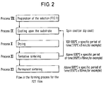
- the sol gel solution obtained in the aforementioned preparatory processes (Figure 1) is coated over a Si substrate by the spin coat method (or the dip coat method) in process IX.
- the coating thickness when dried may be 2000 ⁇ .
- the substrate, onto which the sol gel solution is coated, is successively dried for 3 min, for example, over a heating block warmed to 100-300°C (170°C, for example) in process X, and a tentative sintering is provided for 10 min, for example, at above 600°C (650°C, for example) in process XI.
- a permanent sintering is provided for 1 h, for example, at above 600°C (650°C, for example) in process XII.
- a thin PZT film with a thickness of 2000 ⁇ was obtained through said procedure.
- An Au upper electrode was formed by the sputtering method at the surface of the thin PZT film obtained; the electrical characteristics measured are indicated in Figures 3-5.
- the measurement voltage is established between ⁇ 1.65 V and ⁇ 4.0 V.
- the capacitance of the thin PZT film formed by the solution based on this invention increases together with the measurement voltage as indicated by the solid lines, displaying characteristic peculiar to the ferroelectric film.
- Figure 4 indicates hysteresis curves that are determined by the C-V curves in Figure 3.
- the remanence value Pr of the thin PZT film based on this invention increases in proportion to the increase in the measurement voltage as indicated by the solid lines, and a value of 19.0-20.0 ⁇ C/cm2 was obtained during a measurement at ⁇ 4 V.
- This remanence density is at the level that allows for the storage of a large amount of electrical charge of 380-400 /fc ⁇ m2 when a capacitor in a nonvolatile memory, which will be described later, is prepared using the thin PZT film. This level far exceeds the 100 fc/ ⁇ m2 that is required.
- the resistance electrical field Ec is small and switching is easy.
- Figure 5 indicates the I-V curve of the thin PZT film. A relatively small value of less than 10 ⁇ 8 A/cm2 was obtained when a positive bias was applied to the upper Au electrode. This indicates that the leakage of current of the thin film formed by the solution prepared based on this invention is substantially small while the commonly reported value is large at 10 ⁇ 6 A/cm2.
- a broken section is produced by forming the aforementioned upper electrode (Pt/Ti) (6) on top of a silicon substrate (1), forming a thin PZT film (7) on the top, and rupturing at the position indicated by line A-A in Figure 6(A).
- Figure 7 indicates SEM (scanning electron microscope) observed pictures of the surface of the thin PZT film based on this invention at the ruptured position. It can be observed that a smooth surface is formed with fine particles uniformly spread all over. It is thought that this brings about the aforementioned excellent characteristics.
- the thin PZT film formed using the sol gel solution based on this invention, is used in a capacitor (stack type, for example) in a dynamic RAM memory cell, for example, which is a nonvolatile memory type.
- An element region separated by a field oxide film (2) is formed at one main face of a P ⁇ type silicon substrate (1), for example, and to which a transfer gate TR, that consists of a MOS transistor and a memory cell M-CEL that consists of a capacitor CAP, are formed.
- a word line WL is formed through a gate oxide film (5) between these regions, with a bit line BL being connected to the drain region (4) through a contact hole (11) in insulation layers (9) and (10) such as SiO2.
- the capacitor CAP is referred to as a stack type.
- a lower electrode (6) is connected to the source region (3) through a contact hole (12) in the insulating layer (10); the PZT ferroelectric film (7) and an upper electrode (8) are successively laminated on top of said lower electrode.
- the ferroelectric film (7) which contains the capacitor CAP, consists of PZT, which is the Pb(Zr, Ti)O3 film formed by the sol gel method using the aforementioned source solution based on this invention.
- the lower electrode (6) consists of a tungsten layer or a titanium layer, for example, with Pt deposited, for example, on top (however, the indication of Pt, for example, is eliminated in the figure).
- the upper electrode (8) that makes contact with the ferroelectric film consists of Pt, Au, or aluminium, for example.
- a field oxide film (2) is formed on top of a P ⁇ -type silicon substrate (wafer) (1) by the selective oxidation process.
- a gate oxide film (5) and a polysilicon word line WL are respectively formed by the thermal oxidation method and the chemical gas-phase growth method.
- an N+-type source region (3) and a drain region (4) are respectively formed through thermal diffusion of N-type impurities such as As.
- a contact hole (12) is formed by photolithography at a SiO2 insulating layer (10) that is deposited onto the entire surface by the chemical gas-phase growth method over a source region (3).
- a lower electrode (6) having a Pt layer on top of the tungsten or titanium layer, is successively formed in a manner such that it forms a junction with the source region (3) at the contact hole (12).
- This can be formed by providing a certain patterning to the tungsten or titanium layer or the Pt surface layer coated onto the entire surface by photolithography.
- a sol gel source solution (17) is coated onto the entire surface including the lower electrode (6) by the spin coat method or the dip coat method.
- This source solution (17) has the same composition as the solution (refer to Figure 1) described above.
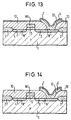
- the wafer coated with the source solution (17) is heated to a specific temperature (100-300°C, 170°C, for example) for 3 min, for example, the coated solution is dried, forming a dry gel film (27) as indicated in Figure 12.
- the wafer is tentatively sintered at a temperature that forms the perovskite crystals (above 600°C, 650°C, for example) for 10 min. It is then permanently sintered (oxidation sintering) at above 600°C (650°C, for example) for 60 min, for example, after repeating the aforementioned drying, with a ferroelectric film (7) being formed onto the entire surface as indicated in Figure 13.
- the ferroelectric film (7) For forming the ferroelectric film (7) at a specific thickness (2000 ⁇ , for example), dry film layers are laminated and the final film thickness can be obtained, without reaching the intended thickness all at once, through repeating the coating process in Figure 11, the drying process in Figure 12, and the aforementioned tentative sintering process as needed.
- the unnecessary portion of the thin ferroelectric film (7) formed onto the entire surface is eliminated by the dry etching method, for example, and the thin PZT ferroelectric film (7) is formed in a specific pattern on top of the lower electrode (6).
- an upper electrode (8) consisting of platinum, for example, is formed in a specific pattern at the junction with the thin ferroelectric film (7) by photolithography.
- interlayer insulating films (10) and (9), a contact hole (11), and a bit line BL are respectively formed by publicly known methods, and a memory cell indicated in Figure 16 is prepared.
- the ferroelectric film (7) of the capacitor CAP in this memory cell is formed using the source solution based on this invention. Therefore, as described above, its film surface is flat, and the electrical characteristics consisting of a large remanence value and a small leakage of current can be obtained.
- fatty acid lead compounds such as lead 2-ethylhexanoate and lead naphthenate can be used as a starting element for preparing the aforementioned sol gel source solution.
- titanium alkoxides such as titaniumtetraethoxide, titaniumtetra-n-butoxide, titanium-n-butoxide, and titanium-tetra-n-pentoxide can be used.
- zirconium alkoxides such as zirconium ⁇ isopropoxide, zirconiumtetraethoxide, zirconium-tetra-n-butoxide, and zirconium-tetra-n-pentoxide can be used.
- Each of these starting elements may be used as in one type or may be a combination of several types.
- each of the dilute alkoxide solutions in the aforementioned processes II and III may be established as mentioned below because the boiling point of isopropyl alcohol is 82.5°C, the boiling point of n-butanol is 98-100°C, and the boiling point of ethyl alcohol is 78.3°C.
- the temperature of the thermal process in the aforementioned processes II to III, the aforementioned process I, and the aforementioned process IV can be established at 70-190°C, 120-180°C, and 120-200°C, respectively.
- n-propanol isopropanol, or n-butanol, for example, can be used as the solvent.
- alkanolamines such as dipropanolamine and triethanolamine or ⁇ -diketones such as acetylacetone, applied jointly, can be used as the stabilizer.
- composition of the ferroelectric substance that can be obtained in this invention may be varied. Also, the application is not limited only to the stack-type capacitors. A structure may be used in which the aforementioned stack-type capacitor is formed on top of a SiO2 film and the lower electrode of said capacitor is extended and connected to the source region of the transfer gate. It can also be applied in a capacitor that is not a stack type, but has a structure in which the capacitor is integrated within a so-called trench (groove).
- the thin PZT film formed from this sol gel solution has sufficient electrical characteristics such as the display of a smooth surface, a large remanence, and a small leakage of current, for example, and satisfies the demanded performance.
Landscapes
- Chemical & Material Sciences (AREA)
- Engineering & Computer Science (AREA)
- Materials Engineering (AREA)
- Mechanical Engineering (AREA)
- Physics & Mathematics (AREA)
- Thermal Sciences (AREA)
- General Chemical & Material Sciences (AREA)
- Chemical Kinetics & Catalysis (AREA)
- Organic Chemistry (AREA)
- Inorganic Chemistry (AREA)
- Metallurgy (AREA)
- Ceramic Engineering (AREA)
- Dispersion Chemistry (AREA)
- Inorganic Compounds Of Heavy Metals (AREA)
- Semiconductor Memories (AREA)
- Chemically Coating (AREA)
- Semiconductor Integrated Circuits (AREA)
Applications Claiming Priority (2)
| Application Number | Priority Date | Filing Date | Title |
|---|---|---|---|
| JP69114/94 | 1994-03-14 | ||
| JP6069114A JPH07252664A (ja) | 1994-03-14 | 1994-03-14 | ゾルーゲル法による強誘電体膜の形成方法、キャパシタの製造方法、その原料溶液の調製方法及びその原料溶液 |
Publications (2)
| Publication Number | Publication Date |
|---|---|
| EP0674019A1 true EP0674019A1 (fr) | 1995-09-27 |
| EP0674019B1 EP0674019B1 (fr) | 1999-06-02 |
Family
ID=13393297
Family Applications (1)
| Application Number | Title | Priority Date | Filing Date |
|---|---|---|---|
| EP95103656A Expired - Lifetime EP0674019B1 (fr) | 1994-03-14 | 1995-03-14 | Dispositifs semi-conducteurs et leurs procédés de fabrication |
Country Status (5)
| Country | Link |
|---|---|
| EP (1) | EP0674019B1 (fr) |
| JP (1) | JPH07252664A (fr) |
| KR (1) | KR950032706A (fr) |
| DE (1) | DE69509959T2 (fr) |
| TW (1) | TW298670B (fr) |
Cited By (10)
| Publication number | Priority date | Publication date | Assignee | Title |
|---|---|---|---|---|
| EP0807965A3 (fr) * | 1996-05-14 | 1998-02-04 | Matsushita Electronics Corporation | Méthode de fabrication d'un couche mince ferroélectrique contenant Bi |
| EP0939434A1 (fr) * | 1998-02-25 | 1999-09-01 | Interuniversitair Micro-Elektronica Centrum Vzw | Méthode de fabrication d'une couche ferroélectrique utilisant la technique sol-gel |
| EP0687750B1 (fr) * | 1994-06-16 | 2000-07-26 | Sharp Kabushiki Kaisha | Procédé de fabrication d'un film mince d'un oxyde composite diélectrique |
| EP0950726A3 (fr) * | 1998-03-31 | 2002-05-02 | KRI International, Inc. | Solution de précurseur d'un film mince en matériau ferro-électrique et procédé de sa production |
| WO2003065438A1 (fr) * | 2002-01-31 | 2003-08-07 | Sharp Kabushiki Kaisha | Solutions de pgo utilisees dans la preparation de films minces de pgo par revetement par centrifugationsolutions de pgo utilisees dans la preparation de films minces de pgo par revetement par centrifugation |
| WO2003102629A3 (fr) * | 2002-05-27 | 2004-10-14 | 4078187 Canada Inc | Guide d'ondes planaire et dispositif optique actifs et passifs a oxyde de metal lourd |
| US7727322B2 (en) | 2004-09-17 | 2010-06-01 | Seiko Epson Corporation | Precursor solution, method for manufacturing precursor solution, PZTN compound oxide, method for manufacturing PZTN compound oxide, piezoelectric element, ink jet printer, ferroelectric capacitor, and ferroelectric memory |
| EP2436661A1 (fr) * | 2008-05-28 | 2012-04-04 | Mitsubishi Materials Corporation | Composition pour la formation d'un film mince ferroélectrique, procédé de formation d'un film mince ferroélectrique et film ferroélectrique formé selon ce procédé |
| US9136541B2 (en) | 2010-02-10 | 2015-09-15 | Showa Denko K.K. | Process for producing fuel cell electrode catalyst, process for producing transition metal oxycarbonitride, fuel cell electrode catalyst and uses thereof |
| US9318749B2 (en) | 2011-01-20 | 2016-04-19 | Showa Denko K.K. | Process for producing catalyst carrier, process for producing composite catalyst, composite catalyst, and fuel cell using same |
Families Citing this family (10)
| Publication number | Priority date | Publication date | Assignee | Title |
|---|---|---|---|---|
| EP1039525A4 (fr) * | 1997-11-10 | 2002-02-06 | Hitachi Ltd | Element dielectrique et mode de fabrication |
| KR100509588B1 (ko) * | 1998-09-28 | 2005-11-25 | 삼성에스디아이 주식회사 | 유기-무기 하이브리드 필름 및 그것을 구비하고 있는 표시소자 |
| JP4269172B2 (ja) * | 2004-12-24 | 2009-05-27 | セイコーエプソン株式会社 | インクジェット塗布用インクおよびその製造方法、ならびに強誘電体膜の製造方法 |
| KR101275609B1 (ko) * | 2005-03-30 | 2013-06-19 | 후지필름 가부시키가이샤 | 용액 캐스팅 방법 |
| JP4900588B2 (ja) * | 2007-01-12 | 2012-03-21 | セイコーエプソン株式会社 | 使用済みコロイド溶液の再生方法 |
| JP5417962B2 (ja) * | 2009-01-20 | 2014-02-19 | 三菱マテリアル株式会社 | 強誘電体薄膜形成用組成物、強誘電体薄膜の形成方法並びに該方法により形成された強誘電体薄膜 |
| JP5293347B2 (ja) * | 2008-12-24 | 2013-09-18 | 三菱マテリアル株式会社 | 強誘電体薄膜形成用組成物、強誘電体薄膜の形成方法並びに該方法により形成された強誘電体薄膜 |
| WO2011089748A1 (fr) | 2010-01-21 | 2011-07-28 | 株式会社ユーテック | Film ferroélectrique de pbnzt, solution sol-gel, procédé de formation de film, et procédé de production d'un film ferroélectrique |
| JP2013136502A (ja) | 2011-11-28 | 2013-07-11 | Mitsubishi Materials Corp | 強誘電体薄膜形成用組成物及びその薄膜の形成方法並びにその方法で形成された薄膜 |
| JP5929654B2 (ja) | 2012-09-11 | 2016-06-08 | 三菱マテリアル株式会社 | 強誘電体薄膜形成用組成物及びその薄膜の形成方法 |
Citations (1)
| Publication number | Priority date | Publication date | Assignee | Title |
|---|---|---|---|---|
| US4946710A (en) * | 1987-06-02 | 1990-08-07 | National Semiconductor Corporation | Method for preparing PLZT, PZT and PLT sol-gels and fabricating ferroelectric thin films |
-
1994
- 1994-03-14 JP JP6069114A patent/JPH07252664A/ja active Pending
-
1995
- 1995-03-14 DE DE69509959T patent/DE69509959T2/de not_active Expired - Fee Related
- 1995-03-14 EP EP95103656A patent/EP0674019B1/fr not_active Expired - Lifetime
- 1995-03-14 KR KR1019950005593A patent/KR950032706A/ko not_active Withdrawn
- 1995-05-15 TW TW084104766A patent/TW298670B/zh active
Patent Citations (1)
| Publication number | Priority date | Publication date | Assignee | Title |
|---|---|---|---|---|
| US4946710A (en) * | 1987-06-02 | 1990-08-07 | National Semiconductor Corporation | Method for preparing PLZT, PZT and PLT sol-gels and fabricating ferroelectric thin films |
Non-Patent Citations (2)
| Title |
|---|
| PAJEWSKI: "pzt coatings prepared by the sol-gel process on metallic substrates (al)", THIRD EURO-CERAMICS, vol. 2, 12 September 1993 (1993-09-12), SPAIN, pages 735 - 738, XP000416124 * |
| VIJAY: "ELECTRODES FOR PZT FERROELECTRIC THIN FILMS", JOURNAL OF THE ELECTROCHEMICAL SOCIETY, vol. 140, no. 9, September 1993 (1993-09-01), USA, pages 2640 - 2645 * |
Cited By (17)
| Publication number | Priority date | Publication date | Assignee | Title |
|---|---|---|---|---|
| EP0687750B1 (fr) * | 1994-06-16 | 2000-07-26 | Sharp Kabushiki Kaisha | Procédé de fabrication d'un film mince d'un oxyde composite diélectrique |
| EP0807965A3 (fr) * | 1996-05-14 | 1998-02-04 | Matsushita Electronics Corporation | Méthode de fabrication d'un couche mince ferroélectrique contenant Bi |
| EP0939434A1 (fr) * | 1998-02-25 | 1999-09-01 | Interuniversitair Micro-Elektronica Centrum Vzw | Méthode de fabrication d'une couche ferroélectrique utilisant la technique sol-gel |
| EP0950726A3 (fr) * | 1998-03-31 | 2002-05-02 | KRI International, Inc. | Solution de précurseur d'un film mince en matériau ferro-électrique et procédé de sa production |
| WO2003065438A1 (fr) * | 2002-01-31 | 2003-08-07 | Sharp Kabushiki Kaisha | Solutions de pgo utilisees dans la preparation de films minces de pgo par revetement par centrifugationsolutions de pgo utilisees dans la preparation de films minces de pgo par revetement par centrifugation |
| WO2003102629A3 (fr) * | 2002-05-27 | 2004-10-14 | 4078187 Canada Inc | Guide d'ondes planaire et dispositif optique actifs et passifs a oxyde de metal lourd |
| US7727322B2 (en) | 2004-09-17 | 2010-06-01 | Seiko Epson Corporation | Precursor solution, method for manufacturing precursor solution, PZTN compound oxide, method for manufacturing PZTN compound oxide, piezoelectric element, ink jet printer, ferroelectric capacitor, and ferroelectric memory |
| US8790538B2 (en) | 2008-05-28 | 2014-07-29 | Mitsubishi Materials Corporation | Composition for ferroelectric thin film formation, method for forming ferroelectric thin film, and ferroelectric thin film formed by the method thereof |
| EP2436661A1 (fr) * | 2008-05-28 | 2012-04-04 | Mitsubishi Materials Corporation | Composition pour la formation d'un film mince ferroélectrique, procédé de formation d'un film mince ferroélectrique et film ferroélectrique formé selon ce procédé |
| US8859051B2 (en) | 2008-05-28 | 2014-10-14 | Mitsubishi Materials Corporation | Composition for ferroelectric thin film formation, method for forming ferroelectric thin film and ferroelectric thin film formed by the method thereof |
| CN104446463A (zh) * | 2008-05-28 | 2015-03-25 | 三菱综合材料株式会社 | 强电介质薄膜形成用组合物、强电介质薄膜的形成方法及通过该方法形成的强电介质薄膜 |
| US9005358B2 (en) | 2008-05-28 | 2015-04-14 | Mitsubishi Materials Corporation | Composition for ferroelectric thin film formation, method for forming ferroelectric thin film, and ferroelectric thin film formed by the method thereof |
| US9502636B2 (en) | 2008-05-28 | 2016-11-22 | Mitsubishi Materials Corporation | Composition for ferroelectric thin film formation, method for forming ferroelectric thin film, and ferroelectric thin film formed by the method thereof |
| CN104446463B (zh) * | 2008-05-28 | 2017-04-12 | 三菱综合材料株式会社 | 强电介质薄膜形成用组合物、强电介质薄膜的形成方法及通过该方法形成的强电介质薄膜 |
| US9136541B2 (en) | 2010-02-10 | 2015-09-15 | Showa Denko K.K. | Process for producing fuel cell electrode catalyst, process for producing transition metal oxycarbonitride, fuel cell electrode catalyst and uses thereof |
| US9318749B2 (en) | 2011-01-20 | 2016-04-19 | Showa Denko K.K. | Process for producing catalyst carrier, process for producing composite catalyst, composite catalyst, and fuel cell using same |
| US9640801B2 (en) | 2011-01-20 | 2017-05-02 | Showa Denko K.K. | Process for producing catalyst carrier, process for producing composite catalyst, composite catalyst, and fuel cell using same |
Also Published As
| Publication number | Publication date |
|---|---|
| DE69509959D1 (de) | 1999-07-08 |
| KR950032706A (ko) | 1995-12-22 |
| JPH07252664A (ja) | 1995-10-03 |
| DE69509959T2 (de) | 1999-11-04 |
| TW298670B (fr) | 1997-02-21 |
| EP0674019B1 (fr) | 1999-06-02 |
Similar Documents
| Publication | Publication Date | Title |
|---|---|---|
| EP0674019A1 (fr) | Dispositifs semi-conducteurs et leurs procédés de fabrication | |
| US5439845A (en) | Process for fabricating layered superlattice materials and making electronic devices including same | |
| EP0766292B1 (fr) | Méthode de fabrication d'un élément à couche ferroélectrique et élément à couche ferroélectrique et élément ferroélectrique fabriqué par cette méthode | |
| US5690727A (en) | Thin films of ABO3 with excess B-site modifiers and method of fabricating integrated circuits with same | |
| EP0665981B1 (fr) | Procede de fabrication de materiaux stratifies a superstructure et de dispositifs electroniques contenant ces derniers | |
| US6072207A (en) | Process for fabricating layered superlattice materials and making electronic devices including same | |
| CN1265224A (zh) | 层状超晶格材料和abo3型金属氧化物的制备方法和在不暴露于氧气下制备包括这些材料的电元件的方法 | |
| US6815223B2 (en) | Low thermal budget fabrication of ferroelectric memory using RTP | |
| KR19980703182A (ko) | 성층 초격자 재료 및 이를 포함하는 전자 소자 제조를 위한저온 처리 | |
| JPH06305713A (ja) | ゾルーゲル法による強誘電体膜の形成方法及びキャパシタの製造方法、及びその原料溶液 | |
| JP2003510839A (ja) | バリア層を有する集積回路およびその製造方法 | |
| US7569400B2 (en) | Ferroelectric film, method of manufacturing ferroelectric film, ferroelectric capacitor, and ferroelectric memory | |
| US20040051129A1 (en) | Metal oxide integrated circuit on silicon germanium substrate | |
| US20040121492A1 (en) | Ferroelectric thin film and method for forming the same | |
| US5776788A (en) | Method for forming a strong dielectric film by the sol-gel technique and a method for manufacturing a capacitor | |
| EP0939434A1 (fr) | Méthode de fabrication d'une couche ferroélectrique utilisant la technique sol-gel | |
| JPH11163273A (ja) | 誘電体薄膜、誘電体キャパシタの製造方法、および誘電体メモリ | |
| US6857172B2 (en) | Method of manufacturing ferroelectric capacitor | |
| KR100252744B1 (ko) | 과잉의 A사이트와 B사이트 개질제(modifier)를 가진 ABO₃의 박막 및 그 박막을 가진 집적회로의 제조방법 | |
| KR19990082374A (ko) | 집적회로에 적용하기 위한 고유전율의 바륨-스트론튬-니오브 | |
| JP2007277082A (ja) | ゾル−ゲル法による強誘電体膜の形成方法及びキャパシタの製造方法 | |
| JP3294214B2 (ja) | 薄膜キャパシタ | |
| JPH10223847A (ja) | 強誘電体薄膜素子の製造方法、強誘電体薄膜素子及び強誘電体メモリ装置 | |
| JPH0536931A (ja) | メモリ素子及びその製造方法 | |
| JPH082919A (ja) | 強誘電体結晶薄膜及び該強誘電体結晶薄膜を有する強誘電体薄膜素子及び該強誘電体結晶薄膜の製造方法 |
Legal Events
| Date | Code | Title | Description |
|---|---|---|---|
| PUAI | Public reference made under article 153(3) epc to a published international application that has entered the european phase |
Free format text: ORIGINAL CODE: 0009012 |
|
| AK | Designated contracting states |
Kind code of ref document: A1 Designated state(s): DE FR GB IT NL |
|
| 17P | Request for examination filed |
Effective date: 19960319 |
|
| 17Q | First examination report despatched |
Effective date: 19970808 |
|
| GRAG | Despatch of communication of intention to grant |
Free format text: ORIGINAL CODE: EPIDOS AGRA |
|
| GRAG | Despatch of communication of intention to grant |
Free format text: ORIGINAL CODE: EPIDOS AGRA |
|
| GRAH | Despatch of communication of intention to grant a patent |
Free format text: ORIGINAL CODE: EPIDOS IGRA |
|
| GRAH | Despatch of communication of intention to grant a patent |
Free format text: ORIGINAL CODE: EPIDOS IGRA |
|
| GRAA | (expected) grant |
Free format text: ORIGINAL CODE: 0009210 |
|
| ITF | It: translation for a ep patent filed | ||
| AK | Designated contracting states |
Kind code of ref document: B1 Designated state(s): DE FR GB IT NL |
|
| PG25 | Lapsed in a contracting state [announced via postgrant information from national office to epo] |
Ref country code: NL Free format text: LAPSE BECAUSE OF FAILURE TO SUBMIT A TRANSLATION OF THE DESCRIPTION OR TO PAY THE FEE WITHIN THE PRESCRIBED TIME-LIMIT Effective date: 19990602 |
|
| REF | Corresponds to: |
Ref document number: 69509959 Country of ref document: DE Date of ref document: 19990708 |
|
| ET | Fr: translation filed | ||
| PLBE | No opposition filed within time limit |
Free format text: ORIGINAL CODE: 0009261 |
|
| STAA | Information on the status of an ep patent application or granted ep patent |
Free format text: STATUS: NO OPPOSITION FILED WITHIN TIME LIMIT |
|
| 26N | No opposition filed | ||
| PG25 | Lapsed in a contracting state [announced via postgrant information from national office to epo] |
Ref country code: FR Free format text: LAPSE BECAUSE OF NON-PAYMENT OF DUE FEES Effective date: 20010531 |
|
| REG | Reference to a national code |
Ref country code: FR Ref legal event code: ST |
|
| REG | Reference to a national code |
Ref country code: FR Ref legal event code: RN Ref country code: FR Ref legal event code: D3 |
|
| REG | Reference to a national code |
Ref country code: GB Ref legal event code: IF02 |
|
| PGFP | Annual fee paid to national office [announced via postgrant information from national office to epo] |
Ref country code: GB Payment date: 20040205 Year of fee payment: 10 |
|
| PGFP | Annual fee paid to national office [announced via postgrant information from national office to epo] |
Ref country code: DE Payment date: 20040331 Year of fee payment: 10 |
|
| PG25 | Lapsed in a contracting state [announced via postgrant information from national office to epo] |
Ref country code: IT Free format text: LAPSE BECAUSE OF NON-PAYMENT OF DUE FEES;WARNING: LAPSES OF ITALIAN PATENTS WITH EFFECTIVE DATE BEFORE 2007 MAY HAVE OCCURRED AT ANY TIME BEFORE 2007. THE CORRECT EFFECTIVE DATE MAY BE DIFFERENT FROM THE ONE RECORDED. Effective date: 20050314 Ref country code: GB Free format text: LAPSE BECAUSE OF NON-PAYMENT OF DUE FEES Effective date: 20050314 |
|
| PG25 | Lapsed in a contracting state [announced via postgrant information from national office to epo] |
Ref country code: DE Free format text: LAPSE BECAUSE OF NON-PAYMENT OF DUE FEES Effective date: 20051001 |
|
| GBPC | Gb: european patent ceased through non-payment of renewal fee |
Effective date: 20050314 |
|
| PG25 | Lapsed in a contracting state [announced via postgrant information from national office to epo] |
Ref country code: FR Free format text: LAPSE BECAUSE OF NON-PAYMENT OF DUE FEES Effective date: 20000331 |