EP0693827A2 - Portes adiabatiques quasi-statiques - Google Patents
Portes adiabatiques quasi-statiques Download PDFInfo
- Publication number
- EP0693827A2 EP0693827A2 EP95304707A EP95304707A EP0693827A2 EP 0693827 A2 EP0693827 A2 EP 0693827A2 EP 95304707 A EP95304707 A EP 95304707A EP 95304707 A EP95304707 A EP 95304707A EP 0693827 A2 EP0693827 A2 EP 0693827A2
- Authority
- EP
- European Patent Office
- Prior art keywords
- gate
- pair
- transistor
- ancillary
- clock signals
- Prior art date
- Legal status (The legal status is an assumption and is not a legal conclusion. Google has not performed a legal analysis and makes no representation as to the accuracy of the status listed.)
- Withdrawn
Links
- 230000000295 complement effect Effects 0.000 claims abstract description 28
- 230000000903 blocking effect Effects 0.000 abstract description 8
- 238000010586 diagram Methods 0.000 description 9
- 230000008859 change Effects 0.000 description 4
- 230000007704 transition Effects 0.000 description 4
- 239000004065 semiconductor Substances 0.000 description 3
- 230000008901 benefit Effects 0.000 description 2
- 230000006870 function Effects 0.000 description 2
- 230000009467 reduction Effects 0.000 description 2
- 230000004044 response Effects 0.000 description 2
- 102000016917 Complement C1 Human genes 0.000 description 1
- 108010028774 Complement C1 Proteins 0.000 description 1
- 230000009471 action Effects 0.000 description 1
- 239000002131 composite material Substances 0.000 description 1
- 230000003292 diminished effect Effects 0.000 description 1
- 230000000694 effects Effects 0.000 description 1
- 238000005516 engineering process Methods 0.000 description 1
- 230000003993 interaction Effects 0.000 description 1
- 239000000463 material Substances 0.000 description 1
- 230000004048 modification Effects 0.000 description 1
- 238000012986 modification Methods 0.000 description 1
- 238000001228 spectrum Methods 0.000 description 1
- 230000000153 supplemental effect Effects 0.000 description 1
Images


Classifications
-
- H—ELECTRICITY
- H03—ELECTRONIC CIRCUITRY
- H03K—PULSE TECHNIQUE
- H03K19/00—Logic circuits, i.e. having at least two inputs acting on one output; Inverting circuits
- H03K19/0008—Arrangements for reducing power consumption
- H03K19/0019—Arrangements for reducing power consumption by energy recovery or adiabatic operation
-
- H—ELECTRICITY
- H03—ELECTRONIC CIRCUITRY
- H03K—PULSE TECHNIQUE
- H03K19/00—Logic circuits, i.e. having at least two inputs acting on one output; Inverting circuits
- H03K19/02—Logic circuits, i.e. having at least two inputs acting on one output; Inverting circuits using specified components
- H03K19/08—Logic circuits, i.e. having at least two inputs acting on one output; Inverting circuits using specified components using semiconductor devices
- H03K19/094—Logic circuits, i.e. having at least two inputs acting on one output; Inverting circuits using specified components using semiconductor devices using field-effect transistors
- H03K19/096—Synchronous circuits, i.e. using clock signals
- H03K19/0963—Synchronous circuits, i.e. using clock signals using transistors of complementary type
Definitions
- the present invention pertains to low-power Semiconductor circuitry. More particularly, the present invention pertains to complementary transistor gates for adiabatic circuits.
- CMOS circuitry that operate with low power requirements are desirable for use in many electronic devices, particularly portable devices that are powered by batteries, solar cells, or other limited-capacity power supplies.
- One of the advantages of CMOS circuitry has been its low rate of power dissipation relative to emitter-coupled logic (ECL), bipolar, and other types of semiconductor circuit devices.
- ECL emitter-coupled logic
- CMOS structral elements are increasingly called upon to perform their switching functions at the high end of the frequency spectrum.
- some recent CMOS circuit designs have wattages more appropriate for the common lightbulb than for submicron, heat-sensitive VLSI semiconductor packages.
- the energy dissipated in switching can be reduced to provide adiabatic performance if logic switching is performed quasi-statically: the dissipation of energy through a dissipative medium is reduced if the transfer is made gradually enough.
- so-called "hot clock” circuits are unconventional circuit designs that apply this principle to provide adiabatic performance. These devices reduce the rate of change in the circuit, but “gradually” is a relative concept.
- Known "hot clock” circuits are capable of operating at frequencies as high as 20 mhz in 0.9 micron CMOS. Under these conditions a 5x to 10x power dissipation reduction can be achieved by hot-clock designs.
- Hot-clock logic designs supply all power to the gates via their clock lines, as described by Seitz, et al. at the Chapel Hill VLSI Conference in 1985. Quasi-static logic operations have two cardinal rules, rules familiar to those in the DC to DC converter art: (1) never enable a switch unless the potential across it is zero; (2) never disable a switch if there is a current flowing through it.
- a CMOS gate in accordance with the present invention includes a gate transistor pair, an output node between the gate transistors in the pair, and a pair of gate clock signals. Each gate clock signal is connected to the source electrode of a respective CMOS gate transistor.
- An ancillary transistor preferably has its channel adapted for connection to the drain of each gate transistor.
- a respective one of a pair of complementary ancillary clock signals is connected to the gate electrode, the "control element" of each respective ancillary transistor.
- Said ancillary clock signals are phase-shifted from the gate clock signals so that said four clock signals have four distinct phases, whereby the gate transistor pair is enabled to establish and maintain full-rail voltage values at the output node.
- these four clock signals are phase-shifted a full 90 degrees from each other.
- the ancillary transistors and offset clock signals of the present invention provide adiabatic performance while producing full-rail voltage swings at gate outputs. In a preferred embodiment this is achieved in homogeneous CMOS device packages. Homogeneous packages are simpler to fabricate than the composite packages required for circuits that include functions such as output level shifting or an asymmetric boost on the clock leads.
- the schottky diodes that are preferable for use as blocking diodes are non-MOS devices and their use can be avoided, for many applications, in accordance with the present invention.
- the interaction of blocking diodes with offset clock signals in accordance with the present invention provides a further reduction of non-adiabatic device charging in a circuit, for specially demanding applications.
- Fig. 1 shows a string of CMOS inverters using two offset trapezoidal "hot clock” signals C1 and C2 , and their complements, to obtain adiabatic operation.
- output waveforms A , B and D do not swing "full rail” through the full voltage range V SS - V DD in response to full-rail swings in the input signal In .
- the input signal that is supplied to the control element of each gate transistor changes during a SETUP PHASE (#1) when the clock signal input to that gate has been entirely disabled, as required for adiabatic operation, and the gate's output floats, as indicated by the dashed line.
- the gate's output is, by then, already floating in midrange rather than holding the full logic values V SS and V DD .
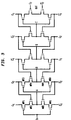
- Fig. 3 shows another serial string of inverters that provides full-rail signal transitions and improved adiabatic performance in accordance with a first embodiment of the present invention.
- each pair of gate clock signals such as C1 and C 1 ⁇
- each gate clock signals is connected to the source electrodes of a respective pair of CMOS gate transistors MP1 and MN1
- the drain electrode of each gate transistor MP1 and MN1 is connected to the gate's output node through ancillary transistors MP2 and MN2 .
- an ancillary transistor MP2 or MN2 is connected between each respective gate clock and the output node.
- the source elctrode of each ancillary transistor, MP2 and MN2 is connected to the drain electrode of the respective gate transistor MP1 or MN1 and the drain electrode is connected to the output node A .
- a respective one of a pair of complementary clock signals C 2 ⁇ and C2 that are offset from the gate clock signals of that gate, C1 and C 1 ⁇ is connected to the gate electrode, the "control element" of each respective ancillary transistor MP2 or MN2 .
- each stage for example C1 or C2 and its complement, is also supplied to a previous stage, a stage that is driven by another, offset clock, C2 or C1 respectively.
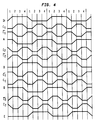
- each ancillary transistor MP2 , MN2 is fully cut off while the gate transistor MP1 , MN1 connected in series with it is in transition in Fig. 4, and the output A remains at its full-rail value.
- This action of the gate's ancillary transistors produces a full-rail voltage swing at output A during the subsequent ENABLE PHASE (#2), as in Fig. 4.
- Fig. 5a shows a CMOS NAND gate circuit in accordance with the present invention.
- Fig. 5b shows a CMOS NOR gate circuit in accordance with the present invention.
- the gate transistors are controlled by the input signals IN1 and IN2 .
- Offset clock C2 and its complement, control the auxiliary transistors MN3 and MP3 , respectively.
- These ancillary transistor pairs prevent the outputs A from following the trapezoidal clocks by disrupting the path to the gates' outputs during the transistions of clock C1 and its inverse, as in Figs. 3 and 4.
- inverters and other gates in accordance with the present invention can be connected in series as shown in Fig. 3, or in parallel as shown in Fig. 5c, or in any combination thereof.
- the gate may be a memory cell, as shown in Fig. 5d.
- the ancillary transistors between the respective gate clocks and the gate output prevent the trapezoidal clocks from wasting power and distorting the output signal, as explained above.
- hot-clock blocking diodes have been added to the circuit shown in Fig. 3 to prevent the non-adiabatic charging that may occur when a gate's input signal does not change.
- This non-adiabatic charging appears at the output nodes in the Fig. 6 timing chart during each gate's SETUP PHASE (#1) when the input signal to the gate is flat, as a low-level signal artifact shown in phantom.
- each ancillary transistor, MP2 and MN2 is connected to the drain electrode of the respective gate transistor MP1 or MN1 and the drain electrode is connected to the output node A .
- a respective one of a pair of complementary clock signals C 2 ⁇ and C2 that are offset from the gate clock signals of that gate, C1 and C 1 ⁇ is connected to the gate electrode, the "control element" of each respective ancillary transistor MP2 or MN2 .
- This remaining artifact can be removed by the use of blocking diodes, while minimizing the negative effects of the blocking diodes by providing a bus for each of four clock buses, for each symmetrical half of the CMOS circuit, as shown in Fig. 7, rather than a diode for each gate transistor.
- This one-diode-per-bus circuit is particularly advantageous when Schottky diodes are used, since Schottky diodes are not MOS devices and are quite expensive to add to an MOS chip.
- MOS diodes do not provide adequate blocking at the low voltage levels where the residual power losses and signal distortions occur in this circuit.
- supplemental diodes are used in circuits operated in accordance with the present invention they would, preferably, be Schottky diodes.
Landscapes
- Engineering & Computer Science (AREA)
- Physics & Mathematics (AREA)
- Computer Hardware Design (AREA)
- Computing Systems (AREA)
- General Engineering & Computer Science (AREA)
- Mathematical Physics (AREA)
- Power Engineering (AREA)
- Logic Circuits (AREA)
- Semiconductor Integrated Circuits (AREA)
Applications Claiming Priority (2)
| Application Number | Priority Date | Filing Date | Title |
|---|---|---|---|
| US276139 | 1988-11-23 | ||
| US27613994A | 1994-07-18 | 1994-07-18 |
Publications (2)
| Publication Number | Publication Date |
|---|---|
| EP0693827A2 true EP0693827A2 (fr) | 1996-01-24 |
| EP0693827A3 EP0693827A3 (fr) | 1997-10-15 |
Family
ID=23055349
Family Applications (1)
| Application Number | Title | Priority Date | Filing Date |
|---|---|---|---|
| EP95304707A Withdrawn EP0693827A3 (fr) | 1994-07-18 | 1995-07-05 | Portes adiabatiques quasi-statiques |
Country Status (4)
| Country | Link |
|---|---|
| US (1) | US5675263A (fr) |
| EP (1) | EP0693827A3 (fr) |
| JP (1) | JPH0865149A (fr) |
| CA (1) | CA2151850A1 (fr) |
Cited By (1)
| Publication number | Priority date | Publication date | Assignee | Title |
|---|---|---|---|---|
| DE19882086B4 (de) * | 1997-02-06 | 2005-06-23 | Intel Corporation, Santa Clara | Verfahren und Vorrichtung zum Implementieren einer adiabatischen Logikfamilie |
Families Citing this family (12)
| Publication number | Priority date | Publication date | Assignee | Title |
|---|---|---|---|---|
| US5473526A (en) | 1994-04-22 | 1995-12-05 | University Of Southern California | System and method for power-efficient charging and discharging of a capacitive load from a single source |
| USRE38918E1 (en) | 1994-04-22 | 2005-12-13 | University Of Southern California | System and method for power-efficient charging and discharging of a capacitive load from a single source |
| US5892372A (en) * | 1997-01-27 | 1999-04-06 | International Business Machines Corporation | Creating inversions in ripple domino logic |
| US5986476A (en) * | 1997-08-08 | 1999-11-16 | Intel Corporation | Method and apparatus for implementing a dynamic adiabatic logic family |
| US5926038A (en) * | 1997-11-10 | 1999-07-20 | The United States Of America As Represented By The Secretary Of The Navy | Two-phase dynamic logic circuits for gallium arsenide complementary HIGFET fabrication |
| US6985142B1 (en) * | 1998-09-03 | 2006-01-10 | University Of Southern California | Power-efficient, pulsed driving of capacitive loads to controllable voltage levels |
| WO2006002075A1 (fr) * | 2004-06-15 | 2006-01-05 | The Regents Of The University Of Michigan | Logique de survoltage de recuperation d'energie |
| US7973565B2 (en) * | 2007-05-23 | 2011-07-05 | Cyclos Semiconductor, Inc. | Resonant clock and interconnect architecture for digital devices with multiple clock networks |
| JP2013507887A (ja) * | 2009-10-12 | 2013-03-04 | サイクロス セミコンダクター, インコーポレイテッド | 共振クロック分配ネットワークの周波数スケール調整された作動のためのアーキテクチャ |
| US9041452B2 (en) * | 2010-01-27 | 2015-05-26 | Silicon Laboratories Inc. | Circuit and method of clocking multiple digital circuits in multiple phases |
| US9985611B2 (en) * | 2015-10-23 | 2018-05-29 | Intel Corporation | Tunnel field-effect transistor (TFET) based high-density and low-power sequential |
| FR3083638B1 (fr) * | 2018-07-06 | 2020-09-25 | Commissariat Energie Atomique | Circuit de memorisation en logique adiabatique capacitive |
Family Cites Families (9)
| Publication number | Priority date | Publication date | Assignee | Title |
|---|---|---|---|---|
| CA945641A (en) * | 1970-04-27 | 1974-04-16 | Tokyo Shibaura Electric Co. | Logic circuit using complementary type insulated gate field effect transistors |
| US3716724A (en) * | 1971-06-30 | 1973-02-13 | Ibm | Shift register incorporating complementary field effect transistors |
| US4164666A (en) * | 1976-06-08 | 1979-08-14 | Toyko Shibaura Electric Co., Ltd. | Electronic apparatus using complementary MOS transistor dynamic clocked logic circuits |
| JPS5829658B2 (ja) * | 1981-02-23 | 1983-06-24 | 株式会社東芝 | 波形変換装置 |
| JPS59134918A (ja) * | 1983-01-24 | 1984-08-02 | Toshiba Corp | ラツチ回路 |
| JPS60145721A (ja) * | 1984-01-10 | 1985-08-01 | Toshiba Corp | フリツプフロツプ回路 |
| JPS6150283A (ja) * | 1984-08-17 | 1986-03-12 | Mitsubishi Electric Corp | シエアドセンスアンプの駆動回路 |
| US4996454A (en) * | 1989-06-30 | 1991-02-26 | Honeywell Inc. | Hot clock complex logic |
| US5003204A (en) * | 1989-12-19 | 1991-03-26 | Bull Hn Information Systems Inc. | Edge triggered D-type flip-flop scan latch cell with recirculation capability |
-
1995
- 1995-06-15 CA CA002151850A patent/CA2151850A1/fr not_active Abandoned
- 1995-07-05 EP EP95304707A patent/EP0693827A3/fr not_active Withdrawn
- 1995-07-18 JP JP7202742A patent/JPH0865149A/ja active Pending
- 1995-11-21 US US08/561,547 patent/US5675263A/en not_active Expired - Fee Related
Cited By (1)
| Publication number | Priority date | Publication date | Assignee | Title |
|---|---|---|---|---|
| DE19882086B4 (de) * | 1997-02-06 | 2005-06-23 | Intel Corporation, Santa Clara | Verfahren und Vorrichtung zum Implementieren einer adiabatischen Logikfamilie |
Also Published As
| Publication number | Publication date |
|---|---|
| CA2151850A1 (fr) | 1996-01-19 |
| JPH0865149A (ja) | 1996-03-08 |
| US5675263A (en) | 1997-10-07 |
| EP0693827A3 (fr) | 1997-10-15 |
Similar Documents
| Publication | Publication Date | Title |
|---|---|---|
| US6404254B2 (en) | Latch circuit and semiconductor integrated circuit having the latch circuit with control signal having a large voltage amplitude | |
| KR100336236B1 (ko) | 반도체집적회로장치 | |
| KR100243850B1 (ko) | 비휘발성 메모리 집적 회로의 고전압 스위칭용고전압 레벨 시프터 | |
| EP0693827A2 (fr) | Portes adiabatiques quasi-statiques | |
| JPS58125298A (ja) | 低消費電力デジタル・レベル・シフタ | |
| JPH09246942A (ja) | 半導体出力回路 | |
| KR20130064006A (ko) | 고전압 영역에서 전력이 공급되고 저전압 영역에서 동작하도록 설계된 소자들로 이루어진 회로에서의 디지털 데이터 처리 | |
| KR101483038B1 (ko) | 전압 레벨 쉬프터 | |
| KR100301151B1 (ko) | 논리증폭기 | |
| JPH0338873A (ja) | 集積回路 | |
| KR100323792B1 (ko) | Mos 트랜지스터 출력 회로 | |
| CN1679236B (zh) | 半导体装置 | |
| CN107534441A (zh) | 电平移位器 | |
| JPH11103240A (ja) | クロック信号レベル変換機能付ラッチ回路及びフリップフロップ回路 | |
| US6249151B1 (en) | Inverter for outputting high voltage | |
| EP0388074A1 (fr) | Circuit CMOS de translation de niveaux logiques | |
| JP3033719B2 (ja) | 低消費電力半導体集積回路 | |
| KR100463246B1 (ko) | 저전력 신호 전달 회로 | |
| KR100261179B1 (ko) | 씨모스 전압 레벨 쉬프트 회로 | |
| JP2003188696A (ja) | 双安定回路 | |
| JP3767697B2 (ja) | 半導体集積回路装置 | |
| KR100256229B1 (ko) | 저전력소모를갖는d-형플립플롭회로 | |
| KR100457343B1 (ko) | 저소비 전류의 더블 버퍼 회로 | |
| JP4134160B2 (ja) | 半導体集積回路装置 | |
| JPH0774620A (ja) | バツフア回路 |
Legal Events
| Date | Code | Title | Description |
|---|---|---|---|
| PUAI | Public reference made under article 153(3) epc to a published international application that has entered the european phase |
Free format text: ORIGINAL CODE: 0009012 |
|
| AK | Designated contracting states |
Kind code of ref document: A2 Designated state(s): DE ES FR GB IT |
|
| PUAL | Search report despatched |
Free format text: ORIGINAL CODE: 0009013 |
|
| AK | Designated contracting states |
Kind code of ref document: A3 Designated state(s): DE ES FR GB IT |
|
| STAA | Information on the status of an ep patent application or granted ep patent |
Free format text: STATUS: THE APPLICATION IS DEEMED TO BE WITHDRAWN |
|
| 18D | Application deemed to be withdrawn |
Effective date: 19980416 |