EP0700204B1 - Appareil de prise de vue avec une échelle dynamique étendue - Google Patents
Appareil de prise de vue avec une échelle dynamique étendue Download PDFInfo
- Publication number
- EP0700204B1 EP0700204B1 EP95306086A EP95306086A EP0700204B1 EP 0700204 B1 EP0700204 B1 EP 0700204B1 EP 95306086 A EP95306086 A EP 95306086A EP 95306086 A EP95306086 A EP 95306086A EP 0700204 B1 EP0700204 B1 EP 0700204B1
- Authority
- EP
- European Patent Office
- Prior art keywords
- signal
- pickup device
- electric charge
- image pickup
- level
- Prior art date
- Legal status (The legal status is an assumption and is not a legal conclusion. Google has not performed a legal analysis and makes no representation as to the accuracy of the status listed.)
- Expired - Lifetime
Links
Images


Classifications
-
- H—ELECTRICITY
- H04—ELECTRIC COMMUNICATION TECHNIQUE
- H04N—PICTORIAL COMMUNICATION, e.g. TELEVISION
- H04N23/00—Cameras or camera modules comprising electronic image sensors; Control thereof
- H04N23/70—Circuitry for compensating brightness variation in the scene
-
- H—ELECTRICITY
- H04—ELECTRIC COMMUNICATION TECHNIQUE
- H04N—PICTORIAL COMMUNICATION, e.g. TELEVISION
- H04N23/00—Cameras or camera modules comprising electronic image sensors; Control thereof
- H04N23/70—Circuitry for compensating brightness variation in the scene
- H04N23/73—Circuitry for compensating brightness variation in the scene by influencing the exposure time
Definitions
- the present invention relates to an imaging apparatus for focusing a light into an image to generate an electric signal representing thus focused light image with a broader dynamic range.
- the conventional imaging apparatus Ic includes an image pickup device 1, an analog signal processor 2, an analog to digital converter 3, and an image pickup device controller 4.
- the image pickup device focuses a light into an object image to produce an electric signal based on thus obtained image.
- the imaging pickup device 1 accumulates the electric charge according to the quantity of light incident thereto for one imaging period.
- the imaging pickup device 1 outputs the accumulated electric charge as an image signal Sd representing the magnitude of thus accumulated electric charge, and further reset the amount of electric charge accumulated therein to zero.
- Figs. 13 and 14 electric charge accumulation characteristics of the image pickup device 1 are shown.
- Fig. 13 shows the quantity of accumulated electric charge with respect to incidental period.
- Fig. 14 shows the quantity of accumulated electric charge with respect to the quantity of incidental light.
- Q0 at the vertical axis indicates a saturation level which is a maximum accumulative electric charge of the image pickup device 1. Note that the amount Dp of incidental light Qinc at the time when the image pickup device reaches the saturation level Q0 represents a dynamic range of the image pickup device.
- the analog signal processor 2 applies various processes such as a noise filtration, a gamma correction, and amplification to the image signal Sd.
- the analog to digital converter 3 converts the electric signal processed by the analog signal processor 2 into a digital signal which will be transferred to the externals.
- the image pickup device controller 4 has an electric charge accumulation controller 4a and an electric charge transmission controller 4b.
- the accumulation controller 4a determines the quantity of the electric charge which the image pickup device 1 accumulates therein.
- the transmission controller 4b controls the image pickup device 1 to transmit the electric charge accumulated therein as a signal Sd to the analog signal processor 2.
- the accumulation controller 4a produces a charge accumulation control signal Sa indicating the quantity of the electric charge to be accumulated in the photo diode of the image pickup device 1.
- the charge accumulation control signal Sa has pulses changing between a first level V0 and a second level V2 in a predetermined period Pv.
- the first level V0 corresponds to the maximum accusative charge corresponding to the saturation level Q0.
- the second level V2 corresponds to "zero" charge level Q2.
- One period between each pulse of the signal Sa corresponds to one vertical blanking period of the image signal Sd.
- the transmission controller 4b produces a first charge transfer signal Sb similar to the charge accumulation control signal Sa.
- the first charge transfer signal Sb has the same frequency as, but is delayed by a predetermined period Ta from the signal Sa.
- the transmission controller 4b further produces a second charge transfer signal Sc which is a combination of plural pulses of vertical transmission signal and horizontal transmission signal. Each batch of plural pulses corresponds to a signal vertical blanking period.
- the photo diode is set to the saturation level Q0 and to zero level Q2 at the leading edge and trailing edge, respectively, of the charge accumulation control signal Sa.
- the photo diode At the trailing edge of the signal Sa, the photo diode begins to accumulate the electric charge, and then transmits the thus accumulated electric charge to the vertical CCD at the leading edge of the signal Sb.
- the photo diode accumulates the electric charge and outputs.
- the vertical CCD On receipt of each pulse of the second charge transfer signal Sc, the vertical CCD outputs the electric charge from the left top to the right bottom thereof, line by line, as the image signal Sd.
- the image pickup device 1 can not accumulate or output the electric charge more than the saturation level Q0 even if the light is being incident thereto over this level Q0.
- the image pickup device 1 when a light stronger than a light level that is determined according to a property of the image pickup device 1 is incident to the pickup device 1, it is impossible to express the strength of that incidental light as the quantity of electric charge accumulated in the image pickup device 1.
- the digital signal output from the A/D converter 3 cannot represent the strength of the light that has been incident to the image pickup device 1 beyond the saturation level Q0 of the image pickup device 1. In other words, it is impossible to reproduce an incidental image light whose brightness band is beyond a brightness range that is determined based on this saturated electric charge quantity. Thus, an imaging apparatus which can reproduce an incidental light with a broader dynamic range is needed.
- EP-A-484135 and EP-A-573235 Improvements to the above described system are disclosed in EP-A-484135 and EP-A-573235.
- the improved systems extend the dynamic range of the imaging apparatus by controlling the amount of electric charge storable by the image pickup device.
- imaging apparatus having an image pickup device for producing an image signal indicative of an object image for a pre-determined imaging period
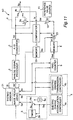
- the imaging apparatus Ip1 includes an image pickup device 1 such as a CCD (charge-coupled device) for focusing a light into an object image to produce an electric signal based on thus obtained image.
- the imaging pickup device 1 accumulates the electric charge according to the quantity of light incident thereto for one imaging period.
- the imaging pickup device 1 outputs the accumulated electric charge as an image signal Sd representing the magnitude of thus accumulated electric charge, and further resets the amount of electric charge accumulated therein to zero.
- An analog signal processor 2 is connected to the image pickup device 1 for receiving the image signal Sd therefrom.
- the analog signal processor 2 applies various processes such as a noise filtering, a gamma correction, and amplification to the image signal Sd.
- An analog to digital (A/D) converter 3 is connected to the analog signal processor 2 for receiving the image signal Sd therefrom.
- the A/D converter 3 converts the image signal Sd processed by the analog signal processor 2 into a digital signal Se.
- An image pickup device controller 4 is provided for controlling the operation of the image pickup device 1.
- the image pickup controller 4 has an electric charge accumulation controller 4a and an electric charge transmission controller 4b.
- the accumulation controller 4a produces a charge accumulation control signal Sa indicating the quantity of the electric charge to be accumulated in the photo diode of the image pickup device 1.
- the signal Sa represents a reference voltage Vsub for the over flow drain (OFD) control of the image pickup device 1.
- the transmission controller 4b produces a first charge transfer signal Sb and a second charge transfer signal Sc.
- An accumulating charge selector 5 is provided between the image pickup device 1 and the electric charge accumulation controller 4a for receiving the charge accumulation control signal Sa.
- the accumulating charge selector 5 includes a first reference voltage source 5a, a timer 5b, and a select switch 5c.
- the first reference voltage source 5a supplies a first reference voltage V1 corresponding to an intermediate level between the first and second levels V0 and V2 (these voltages will be explained below with reference to Fig. 16).
- the timer 5b is connected to the controller 4a for receiving the signal Sa (see Fig. 16) therefrom to produce a selection signal Ss indicating either one of the levels Sa or V1.
- the select switch 5c is connected to the timer 5b for receiving the selection signal Ss.
- the switch 5c selects either one of the electric charge accumulation controller 4a and the first reference voltage source 5a (based on the selection signal Ss) to apply the selected signal Sa or V1 to the image pickup device 1.
- an modified charge accumulation control signal Sa' which sequentially changes its level from the level V1 to level V2 through the predetermined period Tc is applied to the image pickup device 1.
- the charge accumulation control signal Sa is a pulse signal having pulses changing between a first level V0 and a second level V2 with a predetermined period Pv.
- the first level V0 corresponds to the maximum accumulative charge corresponding to the saturation level Q0.
- the second level V2 corresponds to "zero" charge level Q2.
- One period Pv between each pulse of the first pulse signal Sa corresponds to one imaging period such as one vertical blanking period of the image signal Sd, and is usually set to 1/60 seconds for example.
- the first charge transfer signal Sb is a pulse signal similar to the charge accumulation control signal Sa, but is delayed by a predetermined period Ta from the signal Sa. For this period Ta, the image pickup device 1 accumulates the electric charge therein.
- the second charge transfer signal Sc is a combination of plural pulses of vertical transmission signal and horizontal transmission signal. Each batch of plural pulses corresponds to the one imaging period Pv.
- the photo diode of the image pickup device 1 is set to the saturation level Q0 and to zero level Q2 at the leading edge and trailing edge, respectively, of the charge accumulation control signal Sa.
- the photo diode At the trailing edge of the signal Sa, the photo diode begins to accumulate the electric charge, and then transmits this accumulated electric charge to the vertical CCD at the leading edge of the signal Sb.
- the photo diode accumulates the electric charge and outputs this.
- the vertical CCD On receipt of each pulse of the second charge transfer signal Sc, the vertical CCD outputs the electric charge from the left top to the right bottom thereof, line by line, as the image signal Sd.
- a pixel counter 6 is connected to the electric charge transmission controller 4b for receiving the signals Sb and Sc therefrom.
- the pixel counter 6 counts the number of pixels based on the horizontal transfer signal of the signal Sc, and is reset by the signal Sb.
- the pixel counter 6 produces an address signal Sad indicative of the address of the current pixel of the image signal Sd.
- a memory 8 is connected to the pixel counter 6 for receiving the address signal Sad therefrom.
- the memory 8 stores the accumulated charge data indicative of the electric charge which is actually accumulated in the image pickup device 1. This accumulated charge data is previously converted from the analog to digital data, and is stored in the memory 8.
- the memory 8 On receipt of the address data Sad, the memory 8 outputs a reference charge signal Sf indicative of a reference amount of the electric charge with respect to the current pixel address.
- the pixel of the signal Se which is currently output from the A/D convertor 3 corresponds to the pixel of the signal Sf which is currently output from the memory 8.
- a comparator 7 is connected to the A/D converter 3 and the memory 8 for receiving the digitised image signal Se and the reference charge signal Sf therefrom, respectively.
- the comparator 7 compares these signals Se and Sf to produces a result signal Sr indicative of the comparison result.
- a first reference value source 11 is provided for applying a first reference value signal indicative of, for example, a mean value of all the pixel data included in the signal Sf.
- the first reference value signal closes to the majority of the pixels within the image actually obtained.
- a subtracter 10 is connected to the memory 8 for receiving the signals Sf therefrom and, and is further connected to the first reference value source 11 for receiving the reference value signal therefrom to produce a subtraction signal Sst indicative of a difference therebetween.
- the first reference value source 11 stores the mean value of all the pixels in the signal Sf, the value of signal Sst is small.
- a noise remover 9 is connected to the A/D converter 3, the comparator 7, and the subtracter 10 for receiving the signals Se, Sr, and Sst therefrom, respectively.
- the noise remover 9 includes a subtracter 9a and a select switch 9b.
- the subtracter 9a is connected to the A/D converter 3 and to the subtracter 10 for subtracting the signal Sst from the digitized image signal Sd to produce a second subtraction signal.
- the select switch 9b is connected to the comparator 7 for selectively connecting the subtracter 9a based on the result signal Sr.
- the switch 9b selects the subtracter 9a to output the subtracted digitized signal (Se - Sst) as a final image signal Sg therefrom.
- the switch 9b selects the converter 3 to output the digitized image signal Se therefrom.
- Fig. 2 the quantity of accumulated electric charge QAC of the image pickup device according to the present invention with respect to incidental period is indicated by a solid line Lb.
- a dot line La indicates the same of the conventional imaging apparatus Ip of Fig. 12.
- the image pickup device linearly increases the accumulative electric charge amount along the line La until the intermediate saturation level Q1 is reached. Thereafter, the image pickup device will not accumulate more than the level Q1 until a predetermined time Tc has passed since the start of the charge accumulating operation. Thereafter, the image pickup device resumes to increase the accumulative charge linearly having the same gradient as the line La. Finally, the image pickup device reaches the saturation level Q0.
- Fig. 3 the quantity of accumulated electric charge QAC of the image pickup device with respect to the quantity of incidental light Qinc is indicated by a solid line Ld.
- a dot line Lc indicates the same of conventional imaging apparatus Ip of Fig. 12.
- the image pickup device 1 linearly increases the accumulative charge amount along the line Lc until reaching the intermediate saturation level Qm. Thereafter, the image pickup device increases the accumulative electric charge linearly at a predetermined rate smaller than that of the conventional line Lc.
- the image pickup device can accumulate the electric charge even after the conventional image pickup device (having no intermediate saturation level Qm) reaches the saturation level Q0.
- the image pickup device 1 has an expanded dynamic range Di by applying the intermediate saturation level Qm. Specifically speaking, by controlling the saturation level of the image pickup device from a first level Qm to a second level Q0, greater than the first level Qm, within one imaging period Pv, the dynamic range of the image pickup device can be expanded.
- the accumulative charge level of the image pickup device 1 is set to the intermediate level Qm, the actual amount of electric charge accumulated in the device 1 is not equal to the amount Qm.
- the actual accumulated charge amount in the device 1 is subject to some error, and differs from the level Qm at which the device 1 is set. This error or difference will act as noise in the image signal Se. According to the present invention, this noise is removed as follows.
- the comparator 7 compares the digitized signal Se with the previously stored actual accumulated charge data with respect to the same pixel based on the address signal Sad from the pixel counter. According to the comparison result indicating the error for the current pixel, a suitable value Sst which is produced by the subtracter 10 and reference value source 11 is added or subtracted from the current signal Sd by the select switch 9b.
- the dynamic range can be expanded without any image degradation.
- accumulating charge selector 5 operates such that the image pickup device 1 sequentially changes its charge accumulative level from the zero level Q2, to the intermediate level Q1 and then to the saturation level Q0 in that order through the predetermined period Tc.
- Fig. 4 the quantity of accumulated electric charge QAC of the image pickup device according to this alternative with respect to incidental period is indicated by a solid line Lf.
- a dot line Le indicates the line Lb of Fig. 2.
- the image pickup device 1 does not accumulate initially and then linearly increases the accumulative charge amount at the same rate as the line Le until reaching the intermediate saturation level Q1. Thereafter, the image pickup device will not accumulate more than the level Q1 until the predetermined time Tc. Thereafter, the image pickup device resumes to increase the accumulative charge linearly along with the line Le. Finally, the image pickup device 1 reaches the saturation level Q0.
- Fig. 5 the quantity of accumulated electric charge QAC of the image pickup device with respect to the quantity of incidental light Qinc is indicated by a solid line Lg.
- a dot line Lh indicates the line Ld of Fig. 3.
- the dynamic range of the image pickup device 1 can be changed actively, compared with the device 1 described with reference to Fig. 3. Furthermore, the time for the device 1 to accumulate the electric charge can be reduced, as best shown in Fig. 4. As a result, it is possible to obtain an image of a moving object without blurring. Specifically speaking, by changing the saturation level of the image pickup device 1 from the zero level Q2 to the first level Qm, and further to the second level Q0 within one imaging period Pv, the dynamic range of the image pickup device can be expanded actively. Thus, an effect of an electric shutter can be realized.
- the imaging apparatus Ip2 has a construction similar to that of Fig. 1, but the following components are additionally provided.
- a second reference value source 13 is provided for supplying a second reference value signal Sh.
- the second reference value may be set to the maximum amount that a video camera in the NTSC signal system can output. This is because the image data greater than the maximum range of a video camera is not useful.
- a second comparator 12 is connected to the output port of noise remover 9 for receiving the digitized image signal Sg therefrom. The comparator 12 is further connected to the second reference value signal Sh which is compared with the signal Sg and produces a second result signal. When the signal Sg is greater than the signal Sh, the second result signal is High (one). When the signal Sg is equal to or smaller than the signal Sh, the second result signal is Low (zero).
- a counter 14 is connected to the second comparator 12 for receiving the second result signal therefrom. Every time the second result signal becomes High (one), the counter 14 counts up by one to produce a counter signal Sn.
- the counter 14 is further connected to the electric charge transmission controller 4b for receiving the signal Sc therefrom. On receipt of each of the plural pulses of vertical transmission signal and horizontal transmission signal included in the signal, the counter 14 outputs the counter signal Sn corresponding to the current pixel
- a second memory 15 is connected to the second counter 14 and the electric charge transmission controller 4b for receiving the counter signal Sn and the signal Sb therefrom, respectively. On receipt of the signal Sb the memory 15 stores the signal Sn. Thereafter, the counter 14 is reset.
- a third reference value source 16 is provided for supplying a third reference signal Sj indicative of a third predetermined reference value indicative of any number of pixels in the image signal Sd. For example, for producing an image signal representing only one or a few spots in a black background like a star in the sky, one or a few number is adapted as the third reference value Sj. For a brighter image, the third reference value is increased. Thus, the third reference value source 16 is set to store any number suitable for the object image.
- a third comparator 17 is connected to the memory 15 for receiving the signal Si therefrom. The comparator 17 is further connected to the third reference value source 16 for receiving the reference signals Sj therefrom to compare with the signal Si, and produces a third result signal.
- the timer 5b of the accumulating charge selector 5 is connected to the third comparator 17 for receiving the third result signal. Based on the third result signal, the timer 5b changes the timing to turn on.
- the signal Si is smaller than the signal Sj
- the turning on timing of the timer 5b is set to the predetermined time Tc.
- the signal Si is greater than the signal Sj
- the turning on timing of the timer 5b is set to a predetermined time Tc' shorter than the time Tc.
- a modified accumulation control signal Sa" is output to the image pickup device 1.
- wave forms of signal Sa", Sb, Sg, Sn, and Si are shown. Every time the signal Sg becomes greater than the signal Sh, the signal Sn is incremented by one. The signal Sn is output to the memory 15 at the leading edge of the signal Sb, so that a value Ah that the counter 14 counted is stored in the memory 15 as the signal Si. Then, the stored value Ah is compared with the signal Sj. When the value Ah is smaller than the signal Sj, the modified accumulation control signal Sa" is changed to the zero level V0 from the first level V1 after the period Tc'. When the value Ah is greater than the signal Sj, the modified accumulation control signal Sa" having the same shape as the signal Sa' is produced.
- the accumulating charge selector 5 changes the time Tc (Tc') for switching the accumulative charge level QAC of the image pickup device 1 from the first level Q1 to the second level Q0. Furthermore, the intermediate level Qm of the image pickup device 1 is changed.
- the components 12, 13, 14, 15, 16, and 17 control the image pickup device 1 to change its dynamic range so that the image signal Se is kept to be smaller than the reference value Sj.
- the dynamic range of the image pickup device 1 can be suitably actively adjusted for a light image incident to the image pickup device 1.
- the accumulating charge selector 5 operates such that the image pickup device 1 sequentially actively changes its charge accumulative level from the intermediate level Q1 to the saturation level Q0 according to the incidental light to the device 1.
- Fig. 7 the quantity of accumulated electric charge QAC of the image pickup device with respect to incidental period is indicated by a solid line Lj.
- a dot line Li indicates the line Lb of Fig. 2 (the first embodiment). As specifically shown by the solid line Lj, the image pickup device 1 stays at the intermediate level Q1 longer than the that of the first embodiment.
- Fig. 8 the quantity of accumulated electric charge QAC of the image pickup device with respect to the quantity of incidental light Qinc is indicated by a solid line Ll.
- a dot line Lk indicates the line Ld of Fig. 3 (the first embodiment).
- Fig. 9 the quantity of accumulated electric charge QAC of the image pickup device with respect to incidental period is indicated by the solid line Lm.
- a dot line Ln indicates the line Lb of Fig. 2 (the first embodiment).
- Fig. 10 the quantity of accumulated electric charge QAC of the image pickup device with respect to the quantity of incidental light Qinc is indicated by the solid line Lo.
- a dot line Lp indicates the line Ld of Fig. 3 (the first embodiment).
- the dynamic range of the image pickup device 1 can be suitably actively adjusted for a light image incident to the image pickup device 1.
- the imaging apparatus Ip3 has a construction similar to that of Fig. 1, but the following components are additionally provided.
- thermo sensor 21 is provide beside the image pickup device 1 for detecting the temperature therearound to produce a temperature signal St.
- a third memory 22 storing a temperature conversion data is connected to the thermo sensor 21 for receiving the temperature signal St.
- the third memory 22 outputs compensation coefficients Stc corresponding to the temperature signal St based on the conversion data therein.
- An adder 23 is provided just after the first memory 8, and is connected to the third memory 22 for receiving the signal Sf and the compensation coefficients Stc therefrom, respectively.
- the adder 23 adds the coefficients to the reference charge signal Sf to produce a compensated reference charge signal Sf' wherein the thermal influence on the obtained image signal is compensated by the coefficients Stc.
- the charge amount that the image pickup device 1 can actually accumulate therein may vary according to its temperature or the ambient temperature.
- the data stored in the first memory 8 is useless as the reference value for the noise removing operation.
- the above components 21, 22, and 23 are provided. Therefore, according to this embodiment, the dynamic range can be improved without image degradation even when the image pickup device used changes its accumulative charge according to the temperature.
- FIG. 18 With reference to Fig. 18, the improved dynamic range of the image pickup device according to the present invention is described.
- Fig. 18 electric charge accumulation characteristics of the image pickup device 1 according to the present invention are shown.
- the quantity of accumulated electric charge QAC of the image pickup device with respect to the quantity of incidental light Qinc is indicated by the solid lines L1 and L2 having inclination angles ⁇ and ⁇ ', respectively.
- the dot line indicates that of the conventional image pickup device having a dynamic range D1.
- the dynamic range D2 of the image pickup device 1 according to the present invention can be obtained as described bellow.
- the dynamic range of the image pickup device can be expanded to express the incidental light thereto having a wider range as an accumulated electric charge amount. Furthermore, it is also possible to control the image pickup device to have the dynamic range suitably enhanced according to the incidental light.
Landscapes
- Engineering & Computer Science (AREA)
- Multimedia (AREA)
- Signal Processing (AREA)
- Transforming Light Signals Into Electric Signals (AREA)
Claims (12)
- Appareil de formation d'image (Ip1, Ip2, Ip3) ayant un dispositif de prise de vue (1) pour produire un signal d'image (Se) représentatif de l'image d'un objet pendant une période de formation d'image prédéterminée (Pv) ;caractérisé en ce que ledit appareil de formation d'image comporte également un moyen comparateur (7) pour comparer ledit signal d'image (Se), qui dépend dudit niveau de quantité de charge électrique accumulée (Q0, Q1), à un signal de référence prédéterminé (Sf) pour produire un signal de commande (Sr) ; etun moyen de commande (4) pour commander le niveau d'une charge électrique (QAC) que ledit dispositif de prise de vue (1) peut accumuler dans celui-ci ; etun moyen de commutation du niveau de charge électrique accumulée (5) pour commuter ledit dispositif de prise de vue (1) à un premier niveau de quantité de charge électrique accumulée (Q1) et à un second niveau de quantité de charge électrique accumulée (Q0) supérieur audit premier niveau de quantité de charge électrique accumulée (Q1) au cours de ladite période de formation d'image (Pv) ;
un moyen de compensation (9) pour compenser ledit signal d'image (Se) sur la base dudit signal de commande (Sr). - Appareil de formation d'image (Ip1, Ip2, Ip3) selon la revendication 1, comprenant en outre une première source de niveau de référence (11) pour stocker la donnée correspondant audit premier niveau de quantité de charge électrique accumulée (Q1) en tant que ledit niveau de référence prédéterminé (Sf).
- Appareil de formation d'image (Ip1, Ip2, Ip3) selon la revendication 2, dans lequel ladite première source de niveau de référence (11) stocke la donnée correspondant à une quantité maximale de charge électrique (QAC) que ledit dispositif de prise de vue (1) peut accumuler.
- Appareil de formation d'image (Ip1, Ip2, Ip3) selon l'une quelconque des revendications précédentes, dans lequel ledit signal de référence prédéterminé (Sf) correspond à une quantité maximale de charge électrique (QAC) que ledit dispositif de prise de vue (1) peut accumuler.
- Appareil de formation d'image (Ip2) selon l'une quelconque des revendications précédentes, comprenant en outre :un second moyen comparateur (12) pour comparer ledit signal d'image (Se) à un signal de référence prédéterminé (Sh) afin de produire un second signal de commande ; etun moyen de commande des instants de commutation pour commander l'instant où ledit moyen de commutation de quantité de charge électrique accumulée (5) fait commuter ledit dispositif de prise de vue (1) sur la base dudit second signal de commande.
- Appareil de formation d'image (Ip2) selon l'une quelconque des revendications 1 à 4, comprenant en outre :un moyen comparateur (12) pour comparer ledit signal d'image (Sg) à un signal de référence prédéterminé (Sh) afin de produire un second signal de commande ; etun moyen de commande du niveau de quantité de charge électrique accumulée (5, 17) pour commander la valeur dudit premier niveau de quantité de charge électrique accumulée (Q1) sur la base dudit second signal de commande.
- Appareil de formation d'image (Ip2) selon la revendication 5 ou 6, dans lequel ledit niveau de référence prédéterminé (Sh) est le niveau maximum que ledit dispositif de prise de vue (1) peut fournir en sortie.
- Appareil de formation d'image (Ip1) selon l'une quelconque des revendications précédentes, dans lequel ledit moyen de commutation de la quantité de charge accumulée (5) fait en outre commuter ledit dispositif de prise de vue (1) à un troisième niveau de quantité de charge électrique accumulée (Q2) inférieur audit premier niveau de quantité de charge électrique accumulée (Q1).
- Appareil de formation d'image (Ip1) selon la revendication 8, dans lequel ledit troisième niveau de quantité de charge électrique accumulée (Q2) correspond à un niveau d'accumulation nul.
- Appareil de formation d'image (Ip1) selon la revendication 8 ou 9, dans lequel ledit moyen de commutation de quantité de charge accumulée (5) fait commuter ledit dispositif de prise de vue (1) entre lesdits troisième (Q2), premier (Q1) et second (Q2) niveaux, dans cet ordre.
- Appareil de formation d'image (Ip3) selon l'une quelconque des revendications précédentes, comprenant en outre :un moyen détecteur de température (21) pour détecter la température dudit dispositif de prise de vue (1) afin de produire un signal de température (St), etun moyen de compensation (22, 23) pour compenser ledit signal d'image (Se) sur la base dudit signal de température (St).
- Appareil de formation d'image (Ip1, Ip2, Ip3) selon l'une quelconque des revendications précédentes, dans lequel ledit second niveau de quantité de charge électrique accumulée (Q0) correspond à la quantité maximale que ledit dispositif de prise de vue (1) peut accumuler.
Applications Claiming Priority (3)
| Application Number | Priority Date | Filing Date | Title |
|---|---|---|---|
| JP206755/94 | 1994-08-31 | ||
| JP20675594 | 1994-08-31 | ||
| JP6206755A JPH089260A (ja) | 1994-04-19 | 1994-08-31 | 固体撮像装置 |
Publications (3)
| Publication Number | Publication Date |
|---|---|
| EP0700204A2 EP0700204A2 (fr) | 1996-03-06 |
| EP0700204A3 EP0700204A3 (fr) | 1996-12-04 |
| EP0700204B1 true EP0700204B1 (fr) | 2000-06-07 |
Family
ID=16528558
Family Applications (1)
| Application Number | Title | Priority Date | Filing Date |
|---|---|---|---|
| EP95306086A Expired - Lifetime EP0700204B1 (fr) | 1994-08-31 | 1995-08-31 | Appareil de prise de vue avec une échelle dynamique étendue |
Country Status (3)
| Country | Link |
|---|---|
| US (1) | US5642163A (fr) |
| EP (1) | EP0700204B1 (fr) |
| DE (1) | DE69517375T2 (fr) |
Families Citing this family (8)
| Publication number | Priority date | Publication date | Assignee | Title |
|---|---|---|---|---|
| DE69519088T2 (de) * | 1995-07-19 | 2001-05-10 | Oce-Technologies B.V., Venlo | Verfahren und System zum Digitalisieren von CCD-Daten |
| US6750906B1 (en) * | 1998-05-08 | 2004-06-15 | Cirrus Logic, Inc. | Histogram-based automatic gain control method and system for video applications |
| DE69941659D1 (de) * | 1998-09-25 | 2010-01-07 | Bae Systems Information | Erweiterung des Dynamikbereichs von CCD-Bildaufnahmevorrichtungen |
| US6069377A (en) * | 1999-05-13 | 2000-05-30 | Eastman Kodak Company | Image sensor incorporating saturation time measurement to increase dynamic range |
| CN100389596C (zh) * | 2001-08-24 | 2008-05-21 | 迪亚洛格半导体有限公司 | 全集成固态成象器和照相机电路及处理来自其信号的方法 |
| US20050057670A1 (en) * | 2003-04-14 | 2005-03-17 | Tull Damon L. | Method and device for extracting and utilizing additional scene and image formation data for digital image and video processing |
| CN1823336A (zh) * | 2003-05-07 | 2006-08-23 | Dvip多媒体股份有限公司 | 消除传感器电平图像失真的方法和装置 |
| US20090102939A1 (en) * | 2007-10-18 | 2009-04-23 | Narendra Ahuja | Apparatus and method for simultaneously acquiring multiple images with a given camera |
Family Cites Families (10)
| Publication number | Priority date | Publication date | Assignee | Title |
|---|---|---|---|---|
| US3953733A (en) * | 1975-05-21 | 1976-04-27 | Rca Corporation | Method of operating imagers |
| US4479062A (en) * | 1981-02-06 | 1984-10-23 | Asahi Kogaku Kogyo Kabushiki Kaisha | Photo-electric conversion device with accumulation time control |
| US4399464A (en) * | 1981-05-04 | 1983-08-16 | General Dynamics, Pomona Division | Signal processor for an array of CID radiation detector elements |
| JPS6465270A (en) * | 1987-09-04 | 1989-03-10 | Matsushita Electric Industrial Co Ltd | Production of sintered zinc oxide film |
| JPH0793706B2 (ja) * | 1988-03-18 | 1995-10-09 | 松下電器産業株式会社 | 撮像装置と電子スチルカメラ |
| KR100188897B1 (ko) * | 1990-01-31 | 1999-06-01 | 이데이 노부유끼 | 고체촬상장치의 화상결합보정회로 |
| US5055667A (en) * | 1990-06-21 | 1991-10-08 | Loral Fairchild Corporation | Non-linear photosite response in CCD imagers |
| US5295001A (en) * | 1990-11-01 | 1994-03-15 | Canon Kabushiki Kaisha | Image sensing apparatus having tone control function |
| US5463421A (en) * | 1992-05-30 | 1995-10-31 | Sony Corporation | Solid-state image apparatus which sweeps out independently ineffective electric charges so that the exposure period can be varied within a range from one field period to one frame period |
| JP2994158B2 (ja) * | 1992-11-24 | 1999-12-27 | 株式会社東芝 | 固体撮像装置 |
-
1995
- 1995-08-31 EP EP95306086A patent/EP0700204B1/fr not_active Expired - Lifetime
- 1995-08-31 US US08/521,970 patent/US5642163A/en not_active Expired - Fee Related
- 1995-08-31 DE DE69517375T patent/DE69517375T2/de not_active Expired - Fee Related
Also Published As
| Publication number | Publication date |
|---|---|
| US5642163A (en) | 1997-06-24 |
| EP0700204A3 (fr) | 1996-12-04 |
| EP0700204A2 (fr) | 1996-03-06 |
| DE69517375T2 (de) | 2001-03-01 |
| DE69517375D1 (de) | 2000-07-13 |
Similar Documents
| Publication | Publication Date | Title |
|---|---|---|
| JP3467780B2 (ja) | ビデオ信号処理装置及び方法 | |
| KR100286069B1 (ko) | 비디오 카메라 | |
| KR100411207B1 (ko) | 디지탈카메라 | |
| US7262793B2 (en) | Imager and image quality correcting method performing correction based on the output of different readout modes | |
| KR100880085B1 (ko) | 촬상 장치 및 노이즈 제거 방법 | |
| US5825415A (en) | Electronic image-movement correcting device with a variable correction step feature | |
| JP2005130045A (ja) | 撮像装置及びこれに用いる撮像素子 | |
| US6839084B1 (en) | Image pickup apparatus capable of switching modes based on signals from photoelectric conversion pixels | |
| JP4742652B2 (ja) | 撮像装置 | |
| JP4763375B2 (ja) | 撮像装置および画像データの補正方法 | |
| EP0700204B1 (fr) | Appareil de prise de vue avec une échelle dynamique étendue | |
| US5477265A (en) | Device for controlling imaging device | |
| JP4367910B2 (ja) | 固体撮像装置 | |
| US5920344A (en) | CCD camera defective pixel compensation using stored gain values | |
| JP3137339B2 (ja) | ダークシェーディング補正回路 | |
| JP4268643B2 (ja) | 撮像装置およびその雑音低減方法 | |
| JP2007300368A (ja) | 固体撮像装置 | |
| JP4237429B2 (ja) | 画像信号処理装置および欠陥画素補正方法 | |
| JP2007027845A (ja) | 撮像装置 | |
| JP2994158B2 (ja) | 固体撮像装置 | |
| CN102007760B (zh) | 图像拾取设备及其噪声减少方法 | |
| US7714891B2 (en) | Imaging apparatus | |
| JP3298211B2 (ja) | ビデオカメラ及びビデオ再生装置 | |
| JP3212858B2 (ja) | 固体撮像装置 | |
| JP3187068B2 (ja) | スメア除去回路 |
Legal Events
| Date | Code | Title | Description |
|---|---|---|---|
| PUAI | Public reference made under article 153(3) epc to a published international application that has entered the european phase |
Free format text: ORIGINAL CODE: 0009012 |
|
| 17P | Request for examination filed |
Effective date: 19950915 |
|
| AK | Designated contracting states |
Kind code of ref document: A2 Designated state(s): DE FR GB |
|
| PUAL | Search report despatched |
Free format text: ORIGINAL CODE: 0009013 |
|
| AK | Designated contracting states |
Kind code of ref document: A3 Designated state(s): DE FR GB |
|
| 17Q | First examination report despatched |
Effective date: 19981208 |
|
| GRAG | Despatch of communication of intention to grant |
Free format text: ORIGINAL CODE: EPIDOS AGRA |
|
| GRAG | Despatch of communication of intention to grant |
Free format text: ORIGINAL CODE: EPIDOS AGRA |
|
| GRAH | Despatch of communication of intention to grant a patent |
Free format text: ORIGINAL CODE: EPIDOS IGRA |
|
| GRAH | Despatch of communication of intention to grant a patent |
Free format text: ORIGINAL CODE: EPIDOS IGRA |
|
| GRAA | (expected) grant |
Free format text: ORIGINAL CODE: 0009210 |
|
| AK | Designated contracting states |
Kind code of ref document: B1 Designated state(s): DE FR GB |
|
| REF | Corresponds to: |
Ref document number: 69517375 Country of ref document: DE Date of ref document: 20000713 |
|
| ET | Fr: translation filed | ||
| PLBE | No opposition filed within time limit |
Free format text: ORIGINAL CODE: 0009261 |
|
| STAA | Information on the status of an ep patent application or granted ep patent |
Free format text: STATUS: NO OPPOSITION FILED WITHIN TIME LIMIT |
|
| 26N | No opposition filed | ||
| REG | Reference to a national code |
Ref country code: GB Ref legal event code: IF02 |
|
| PGFP | Annual fee paid to national office [announced via postgrant information from national office to epo] |
Ref country code: FR Payment date: 20040810 Year of fee payment: 10 |
|
| PGFP | Annual fee paid to national office [announced via postgrant information from national office to epo] |
Ref country code: GB Payment date: 20040825 Year of fee payment: 10 |
|
| PGFP | Annual fee paid to national office [announced via postgrant information from national office to epo] |
Ref country code: DE Payment date: 20040902 Year of fee payment: 10 |
|
| PG25 | Lapsed in a contracting state [announced via postgrant information from national office to epo] |
Ref country code: GB Free format text: LAPSE BECAUSE OF NON-PAYMENT OF DUE FEES Effective date: 20050831 |
|
| PG25 | Lapsed in a contracting state [announced via postgrant information from national office to epo] |
Ref country code: DE Free format text: LAPSE BECAUSE OF NON-PAYMENT OF DUE FEES Effective date: 20060301 |
|
| GBPC | Gb: european patent ceased through non-payment of renewal fee |
Effective date: 20050831 |
|
| PG25 | Lapsed in a contracting state [announced via postgrant information from national office to epo] |
Ref country code: FR Free format text: LAPSE BECAUSE OF NON-PAYMENT OF DUE FEES Effective date: 20060428 |
|
| REG | Reference to a national code |
Ref country code: FR Ref legal event code: ST Effective date: 20060428 |