EP0714169A1 - Schaltung zur Klemmung eines Signals auf einen Referenzwert - Google Patents
Schaltung zur Klemmung eines Signals auf einen Referenzwert Download PDFInfo
- Publication number
- EP0714169A1 EP0714169A1 EP95410130A EP95410130A EP0714169A1 EP 0714169 A1 EP0714169 A1 EP 0714169A1 EP 95410130 A EP95410130 A EP 95410130A EP 95410130 A EP95410130 A EP 95410130A EP 0714169 A1 EP0714169 A1 EP 0714169A1
- Authority
- EP
- European Patent Office
- Prior art keywords
- converter
- reference value
- output
- nref
- value
- Prior art date
- Legal status (The legal status is an assumption and is not a legal conclusion. Google has not performed a legal analysis and makes no representation as to the accuracy of the status listed.)
- Granted
Links
Images

Classifications
-
- H—ELECTRICITY
- H03—ELECTRONIC CIRCUITRY
- H03M—CODING; DECODING; CODE CONVERSION IN GENERAL
- H03M1/00—Analogue/digital conversion; Digital/analogue conversion
- H03M1/12—Analogue/digital converters
- H03M1/124—Sampling or signal conditioning arrangements specially adapted for A/D converters
- H03M1/129—Means for adapting the input signal to the range the converter can handle, e.g. limiting, pre-scaling ; Out-of-range indication
- H03M1/1295—Clamping, i.e. adjusting the DC level of the input signal to a predetermined value
-
- H—ELECTRICITY
- H04—ELECTRIC COMMUNICATION TECHNIQUE
- H04N—PICTORIAL COMMUNICATION, e.g. TELEVISION
- H04N5/00—Details of television systems
- H04N5/14—Picture signal circuitry for video frequency region
- H04N5/16—Circuitry for reinsertion of DC and slowly varying components of signal; Circuitry for preservation of black or white level
- H04N5/18—Circuitry for reinsertion of DC and slowly varying components of signal; Circuitry for preservation of black or white level by means of "clamp" circuit operated by switching circuit
Definitions
- the present invention relates to a circuit for slaving a signal to a continuous reference value during successive time intervals in order to regularly restore a basic level of the signal.
- the present invention relates more particularly to such a control circuit making it possible, in a television set, to restore the black level of a chrominance or luminance signal after line returns.
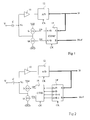
- FIG. 1 represents a conventional circuit for controlling a luminance or chrominance signal on the black level.
- the non-controlled signal V is applied to the input of an amplifier 10 via a capacitor C.
- the signal Vc at the input of the amplifier 10 corresponds to the signal to be controlled on the black level.
- This signal Vc, amplified by the amplifier 10 is most often converted to digital by an analog / digital converter 12.
- a digital comparator 14 receives on an input A the digital output N of the converter 12 and on an input B a digital value reference Nref.
- the terminal of the capacitor C, from which the slave signal Vc is taken, is connected to a high supply potential Vdd by a load current source Ic, and to the GND ground by a discharge current source Id.
- the charge source Ic is activated by a signal UP delivered by the comparator 14 when the value N is less than Nref.
- the source Id is activated by a signal DN delivered by the comparator 14 when the value N is greater than Nref.
- the source Ic or Id is activated at the rate of a clock CK supplied to the comparator 14 and to the converter 12.
- This circuit is only used during line returns; for the duration of the lines, the current sources Ic and Id are deactivated.
- the voltage V is assumed to be constant. In practice, this voltage V includes noise caused by various surrounding parasitic phenomena. This noise is directly transmitted by the capacitor C and the amplifier 10 to the input of the converter 12 and can cause a modification of the digital signal N.
- the noise which is random and of zero mean value, is not annoying in a loop open, that is to say outside the control phases.
- the circuit performs a correction of the signal N at each clock cycle as a function of the value of the signal N found in the previous cycle.
- a spurious pulse of the voltage Vc causes an increase in the value N
- the circuit performs, in the next cycle, a negative correction of the voltage Vc, even if this voltage Vc simultaneously undergoes a negative spurious pulse : the negative correction and the negative parasitic pulse are cumulated and increase the error of the value N rather than decreasing it.
- Such cumulative errors have a non-negligible probability of occurring and cause an oscillation of the signal N with an amplitude of several units. While an oscillation of one unit is normal and tolerable, an oscillation of several units becomes visible on the screen and deteriorates the image quality.
- the converter 12 generally used in such a circuit is a converter which has a latency of several clock cycles CK, often three, between the moment when a sample of the input signal of the converter is acquired and the 'moment when the numerical value of this sample is provided by the converter.
- CK clock cycles
- a charge or discharge current is applied to the capacity C during all these latency cycles.
- the voltage Vc could reach the desired value during the first of the following latency cycles. If this happens, the correction still continues to be carried out during the remaining latency cycles, which again moves the value Vc from the desired value.
- this distance from the voltage Vc is likely to be sufficient to modify the value N in the wrong direction. This also results in an oscillation of the signal N (and of the value Vc) with an amplitude which may become visible on the screen.
- An object of the present invention is to provide a circuit for controlling a signal on a reference value, which is not very sensitive to noise.
- Another object of the present invention is to provide such a circuit which does not oscillate due to the latency time of an analog / digital converter.
- a circuit for controlling an analog signal to a reference value comprising an analog / digital converter receiving the analog signal modified by the charge stored in a capacity.
- a digital comparator receives the output of the converter and a digital reference value, and controls sources of charge and discharge of the capacity.
- a memory point represents a stability condition flag to inhibit charging and discharging of the capacity.
- a converter output analysis circuit activates the flag when the successive values of the converter output satisfy a predetermined stability condition, and deactivates the flag when the successive values of the converter output satisfy a predetermined divergence condition .
- the circuit comprises a window detector, active when the output of the converter is in the vicinity of the reference value, to reduce the amount of charge or discharge of the capacitor.
- the reduced amount of charge or discharge is such that the output of the converter varies by at most one unit from one value to the next.
- the circuit comprises a drift detector for, when the successive values of the output of the converter satisfy a predetermined drift condition and while said flag is active, applying a charge or discharge of quantity scaled down.
- the window of the window detector is delimited by the reference value increased by one and by the reference value decreased by one.
- the stability condition corresponds to two consecutive values equal to the reference value
- the divergence condition corresponds to four consecutive values greater or less than the reference value
- the drift condition corresponds to three consecutive values greater or less than the reference value, the second value among these three values possibly being equal to the reference value.
- FIG. 2 shows the same elements as in Figure 1, designated by the same references.
- These four signals are supplied, according to the invention, to a control circuit 16 which analyzes these signals and controls the current sources Ic and Id (by the signals UP and DN) in the manner described below.
- the circuit of FIG. 2 operates initially like that of FIG. 1 as long as the control circuit 16 detects that the values N and Nref are different. As soon as the signal N stabilizes at Nref, the control circuit 16 enters a locked mode where the sources Ic and Id are no longer activated. In this case, even if the signal Vc or N varies randomly due to noise, the circuit does not make any correction which could cause the signals Vc and N to oscillate.
- the circuit has a rapid convergence mode when the signal N is distant from Nref, and a fine convergence mode when the signal N differs from Nref by one unit.
- the fine correction is chosen to be sufficiently weak so that the signal N does not vary during the latency cycles of the converter 12, which avoids an entry into oscillation of the signal Vc or N.
- this fine correction is also used when the control circuit 16, being in locked mode, detects a condition of low drift insufficient to switch the mode.
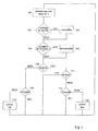
- FIG. 3 represents a flowchart illustrating in more detail the operation of the control circuit 16 according to the first embodiment.
- a paragraph describing a flowchart block begins with the block number.
- the last N values are analyzed to determine if they satisfy a stability condition. This stability condition is satisfied, for example, if the last two values N are equal to Nref.
- a stability condition is satisfied, for example, if the last two values N are equal to Nref.
- the circuit goes into a locked mode indicated, for example, by a flag corresponding to the state of a memory point (a flip-flop).
- the last N values are analyzed to determine if they satisfy a divergence condition. This condition is satisfied, for example, if the last four values of N are either all greater or all less than Nref.
- a divergence condition is satisfied, for example, if the last four values of N are either all greater or all less than Nref.
- the divergence condition is satisfied if these four couples are all equal to (1.0) or to (0.0).
- the circuit goes into unlocked mode by a validation of the flag which had been validated at block 104.
- the value N is strictly greater than Nref. We check if the circuit is in locked mode. If so, the value N is slightly greater than Nref and the difference is only a parasitic phenonema which should not be corrected. The circuit waits for a new value N at block 100.
- the circuit is not in locked mode.
- the signal N is in phase of convergence decreasing towards Nref, or has reached Nref but begins to diverge in increasing.
- the signal DN is activated during a clock cycle, which causes the discharge of the capacity C by the source Id of an amount determined by the current of the source Id, the period of the clock CK, and the value of capacity C.
- Symmetric operations are performed if the value N is less than Nref. It is checked in a block 114 ', as in block 114, if the circuit is locked. In the affirmative, no correction is made and a new value N is awaited at block 100. If not, the signal UP is activated in a block 116 ′ during a clock cycle to charge the capacitance C of a predetermined amount.
- Blocks 102 to 108 which are used to put the circuit in locked or unlocked mode, have been integrated in the flow diagram of FIG. 3. However, the corresponding operations can be carried out separately, in parallel with the rest of the operations of the organization chart.
- the control circuit according to the invention does not correct random interference of the signal Vc or N, once the signal N has reached Nref.
- the signal Vc or N is again corrected only if it has divergence characteristics (several successive values greater or less than the desired value).
- FIG. 4 partially represents a flowchart, starting from block 110 of the flowchart of FIG. 3, illustrating an optimized operation of the control circuit according to the invention. This flow chart comprises all the blocks of FIG. 3 which are not described again.
- N is strictly greater than Nref and it is checked whether it is equal to Nref + 1. If not, the operations continue, as previously described, at block 114 to carry out, if necessary, a normal correction.
- N is equal to Nref + 1.
- the circuit is not in locked mode. At this stage, this means either that the signal N is converging in decreasing direction towards Nref and is in the vicinity of Nref, or that the signal N begins to diverge in increasing direction. A fine correction is then made.
- the capacity C is discharged by a reduced quantity compared to that of the block 116.
- the signal DN is activated only during an alternation of the clock CK, that is to say say for half a clock period or even less if the duty cycle of the clock is chosen to be less than 0.5.
- the optimal value of this reduced discharge is such that the voltage Vc does not reach a value corresponding to Nref-1 during the latency cycles of the converter. This thus eliminates the oscillations due to too large corrections made in the vicinity of Nref. Rapid convergence is also ensured by blocks 114 and 116 when the signal N is far from Nref.
- the circuit is in locked mode and the value N is equal to Nref + 1.
- Nref + 1 we check if the last values N satisfy to a positive drift condition which is insufficient to trigger the unlocking of the circuit. This drift condition corresponds, for example, to three consecutive values equal to Nref + 1, that of the medium possibly being equal to Nref. If so, a decision is made to make a correction, but a fine correction is made in block 122. In the negative, no correction is made and a new value N is expected in block 100.
Landscapes
- Engineering & Computer Science (AREA)
- Multimedia (AREA)
- Signal Processing (AREA)
- Theoretical Computer Science (AREA)
- Processing Of Color Television Signals (AREA)
- Picture Signal Circuits (AREA)
- Color Television Systems (AREA)
- Stabilization Of Oscillater, Synchronisation, Frequency Synthesizers (AREA)
- Manipulation Of Pulses (AREA)
- Analogue/Digital Conversion (AREA)
Applications Claiming Priority (2)
| Application Number | Priority Date | Filing Date | Title |
|---|---|---|---|
| FR9414414 | 1994-11-25 | ||
| FR9414414A FR2727595A1 (fr) | 1994-11-25 | 1994-11-25 | Circuit d'asservissement d'un signal sur une valeur de preference |
Publications (2)
| Publication Number | Publication Date |
|---|---|
| EP0714169A1 true EP0714169A1 (de) | 1996-05-29 |
| EP0714169B1 EP0714169B1 (de) | 2001-09-05 |
Family
ID=9469349
Family Applications (1)
| Application Number | Title | Priority Date | Filing Date |
|---|---|---|---|
| EP95410130A Expired - Lifetime EP0714169B1 (de) | 1994-11-25 | 1995-11-23 | Schaltung zur Klemmung eines Signals auf einen Referenzwert |
Country Status (5)
| Country | Link |
|---|---|
| US (1) | US5731771A (de) |
| EP (1) | EP0714169B1 (de) |
| JP (1) | JP2947149B2 (de) |
| DE (1) | DE69522536D1 (de) |
| FR (1) | FR2727595A1 (de) |
Cited By (6)
| Publication number | Priority date | Publication date | Assignee | Title |
|---|---|---|---|---|
| FR2762162A1 (fr) * | 1997-04-15 | 1998-10-16 | Philips Electronics Nv | Dispositif d'alignement numerique |
| EP0920195A1 (de) * | 1997-11-28 | 1999-06-02 | Koninklijke Philips Electronics N.V. | Vorrichtung zum Gewinnen und Verstärken von elektronischen Signalen |
| WO2000014883A3 (de) * | 1998-09-04 | 2000-05-25 | Infineon Technologies Ag | Differentielle eingangsschaltung für ein digitales signalverarbeitungssystem |
| EP0944246A3 (de) * | 1998-03-18 | 2001-03-21 | Nec Corporation | Klemmschaltung |
| EP1313309A1 (de) * | 2001-11-19 | 2003-05-21 | STMicroelectronics S.A. | Kalibriervorrichtung für eine Video-Eingangsstufe |
| CN108347247A (zh) * | 2012-09-07 | 2018-07-31 | 三星电子株式会社 | 图像传感器 |
Families Citing this family (3)
| Publication number | Priority date | Publication date | Assignee | Title |
|---|---|---|---|---|
| JP2000278132A (ja) * | 1999-03-24 | 2000-10-06 | Matsushita Electric Ind Co Ltd | 多信号のクランプ装置 |
| FR2835327B1 (fr) * | 2002-01-31 | 2004-08-27 | St Microelectronics Sa | Dispositif de calibrage pour un etage d'entree video |
| EP2421281A3 (de) * | 2010-08-17 | 2012-04-04 | Nxp B.V. | Schaltung und Verfahren zur Überwachung einer kapazitativen Signalquelle |
Citations (4)
| Publication number | Priority date | Publication date | Assignee | Title |
|---|---|---|---|---|
| JPS61210770A (ja) * | 1985-03-15 | 1986-09-18 | Hitachi Ltd | クランプ回路 |
| EP0220894A2 (de) * | 1985-10-21 | 1987-05-06 | Rank Cintel Limited | Klemmschaltung für einen Analog-zu-Digital-Wandler |
| EP0280123A1 (de) * | 1987-02-13 | 1988-08-31 | Fujitsu Limited | Spannungspegelklemmschaltung |
| JPH0335666A (ja) * | 1989-06-30 | 1991-02-15 | Mitsubishi Electric Corp | 映像信号クランプ回路 |
Family Cites Families (5)
| Publication number | Priority date | Publication date | Assignee | Title |
|---|---|---|---|---|
| JPS62122465A (ja) * | 1985-11-22 | 1987-06-03 | Nec Corp | クランプ回路 |
| JPS63204975A (ja) * | 1987-02-20 | 1988-08-24 | Fujitsu Ltd | 信号レベルクランプ回路 |
| JP3143117B2 (ja) * | 1990-09-25 | 2001-03-07 | キヤノン株式会社 | 信号処理装置 |
| JP2731641B2 (ja) * | 1991-07-25 | 1998-03-25 | 日本電気株式会社 | 映像アナログディジタル変換器 |
| KR950007419A (ko) * | 1993-08-19 | 1995-03-21 | 김광호 | 적응적 클램핑 회로 |
-
1994
- 1994-11-25 FR FR9414414A patent/FR2727595A1/fr active Granted
-
1995
- 1995-11-16 JP JP7321300A patent/JP2947149B2/ja not_active Expired - Lifetime
- 1995-11-21 US US08/561,522 patent/US5731771A/en not_active Expired - Lifetime
- 1995-11-23 DE DE69522536T patent/DE69522536D1/de not_active Expired - Lifetime
- 1995-11-23 EP EP95410130A patent/EP0714169B1/de not_active Expired - Lifetime
Patent Citations (4)
| Publication number | Priority date | Publication date | Assignee | Title |
|---|---|---|---|---|
| JPS61210770A (ja) * | 1985-03-15 | 1986-09-18 | Hitachi Ltd | クランプ回路 |
| EP0220894A2 (de) * | 1985-10-21 | 1987-05-06 | Rank Cintel Limited | Klemmschaltung für einen Analog-zu-Digital-Wandler |
| EP0280123A1 (de) * | 1987-02-13 | 1988-08-31 | Fujitsu Limited | Spannungspegelklemmschaltung |
| JPH0335666A (ja) * | 1989-06-30 | 1991-02-15 | Mitsubishi Electric Corp | 映像信号クランプ回路 |
Non-Patent Citations (2)
| Title |
|---|
| PATENT ABSTRACTS OF JAPAN vol. 011, no. 046 (E - 479) 12 February 1987 (1987-02-12) * |
| PATENT ABSTRACTS OF JAPAN vol. 015, no. 165 (E - 1061) 25 April 1991 (1991-04-25) * |
Cited By (12)
| Publication number | Priority date | Publication date | Assignee | Title |
|---|---|---|---|---|
| FR2762162A1 (fr) * | 1997-04-15 | 1998-10-16 | Philips Electronics Nv | Dispositif d'alignement numerique |
| EP0872960A1 (de) * | 1997-04-15 | 1998-10-21 | Koninklijke Philips Electronics N.V. | Digitale Abgleichanordnung |
| US6118830A (en) * | 1997-04-15 | 2000-09-12 | U.S. Philips Corporation | Digital DC restoration device |
| EP0920195A1 (de) * | 1997-11-28 | 1999-06-02 | Koninklijke Philips Electronics N.V. | Vorrichtung zum Gewinnen und Verstärken von elektronischen Signalen |
| EP0944246A3 (de) * | 1998-03-18 | 2001-03-21 | Nec Corporation | Klemmschaltung |
| WO2000014883A3 (de) * | 1998-09-04 | 2000-05-25 | Infineon Technologies Ag | Differentielle eingangsschaltung für ein digitales signalverarbeitungssystem |
| US6552592B1 (en) | 1998-09-04 | 2003-04-22 | Micronas Gmbh | Differential input circuit for digital signal processing system |
| EP1313309A1 (de) * | 2001-11-19 | 2003-05-21 | STMicroelectronics S.A. | Kalibriervorrichtung für eine Video-Eingangsstufe |
| FR2832579A1 (fr) * | 2001-11-19 | 2003-05-23 | St Microelectronics Sa | Dispositif de calibrage pour un etage d'entree video |
| US7050116B2 (en) | 2001-11-19 | 2006-05-23 | Stmicroelectronics, S.A. | Calibration device for a video input stage |
| CN108347247A (zh) * | 2012-09-07 | 2018-07-31 | 三星电子株式会社 | 图像传感器 |
| CN108347247B (zh) * | 2012-09-07 | 2021-08-31 | 三星电子株式会社 | 图像传感器 |
Also Published As
| Publication number | Publication date |
|---|---|
| FR2727595A1 (fr) | 1996-05-31 |
| JP2947149B2 (ja) | 1999-09-13 |
| EP0714169B1 (de) | 2001-09-05 |
| FR2727595B1 (de) | 1997-02-14 |
| US5731771A (en) | 1998-03-24 |
| JPH08228303A (ja) | 1996-09-03 |
| DE69522536D1 (de) | 2001-10-11 |
Similar Documents
| Publication | Publication Date | Title |
|---|---|---|
| US7391452B2 (en) | Successive approximation calibration apparatus, system, and method for dynamic range extender | |
| US4783701A (en) | Focus condition detecting device for use in a camera | |
| EP0714169A1 (de) | Schaltung zur Klemmung eines Signals auf einen Referenzwert | |
| FR2816131A1 (fr) | Generateur de fonction avec frequence d'oscillation reglable | |
| FR2798791A1 (fr) | Convertisseur numerique-analogique en courant | |
| EP0718887A1 (de) | Abgleichschaltung für Widerstände | |
| EP3667275B1 (de) | Temperatursensor | |
| FR2959367A1 (fr) | Circuit tampon pour charge capacitive de forte valeur | |
| EP1484910A1 (de) | Adaptive redundante A/D Umsetzungsvorrichtung und -verfahren für Bildaufnahmesensor | |
| EP1071213B1 (de) | Steuerung eines MOS-Leistungstransistors | |
| EP0317421B1 (de) | Analog/Digital-Umwandler vom parallelen Typ | |
| EP2327160B1 (de) | Analogzähler und ein einen solchen zähler enthaltenden bildgeber | |
| EP0346988A2 (de) | Integrierte Halbleiterschaltung mit synchronisiertem Komparator | |
| EP0625849B1 (de) | Schaltungsanordnung zum Einstellen des Schwarzwertes eines Videosignals | |
| JP3985897B2 (ja) | 画像センサの暗レベル決定回路 | |
| EP0959630B1 (de) | Schaltung zum Regulieren der Chrominanzsignalamplitude | |
| EP0644654A1 (de) | Digitaler Integrator und Filter erster Ordnung | |
| US4862273A (en) | Focus condition detecting device for use in a camera | |
| FR2829318A1 (fr) | Boucle a verrouillage de phase realisee sous forme de circuit integre | |
| FR2758021A1 (fr) | Circuit elevateur de tension | |
| EP0848547B1 (de) | Schnittstellenschaltung für Videokamera | |
| EP0952740B1 (de) | Demodulator, insbesondere von SECAM-Chrominanzsignal, mit Frequenzdoppelabstimmungsvorrichtung | |
| FR2943179A1 (fr) | Capteur d'image mos et procede de lecture avec transistor en regime de faible inversion. | |
| EP4002689A1 (de) | Oszillator | |
| FR2725327A1 (fr) | Circuit compteur ayant une fonction de chargement |
Legal Events
| Date | Code | Title | Description |
|---|---|---|---|
| PUAI | Public reference made under article 153(3) epc to a published international application that has entered the european phase |
Free format text: ORIGINAL CODE: 0009012 |
|
| AK | Designated contracting states |
Kind code of ref document: A1 Designated state(s): DE FR GB IT |
|
| 17P | Request for examination filed |
Effective date: 19961106 |
|
| RAP3 | Party data changed (applicant data changed or rights of an application transferred) |
Owner name: STMICROELECTRONICS S.A. |
|
| 17Q | First examination report despatched |
Effective date: 19990720 |
|
| GRAG | Despatch of communication of intention to grant |
Free format text: ORIGINAL CODE: EPIDOS AGRA |
|
| GRAG | Despatch of communication of intention to grant |
Free format text: ORIGINAL CODE: EPIDOS AGRA |
|
| GRAH | Despatch of communication of intention to grant a patent |
Free format text: ORIGINAL CODE: EPIDOS IGRA |
|
| GRAH | Despatch of communication of intention to grant a patent |
Free format text: ORIGINAL CODE: EPIDOS IGRA |
|
| GRAA | (expected) grant |
Free format text: ORIGINAL CODE: 0009210 |
|
| AK | Designated contracting states |
Kind code of ref document: B1 Designated state(s): DE FR GB IT |
|
| PG25 | Lapsed in a contracting state [announced via postgrant information from national office to epo] |
Ref country code: IT Free format text: LAPSE BECAUSE OF FAILURE TO SUBMIT A TRANSLATION OF THE DESCRIPTION OR TO PAY THE FEE WITHIN THE PRESCRIBED TIME-LIMIT;WARNING: LAPSES OF ITALIAN PATENTS WITH EFFECTIVE DATE BEFORE 2007 MAY HAVE OCCURRED AT ANY TIME BEFORE 2007. THE CORRECT EFFECTIVE DATE MAY BE DIFFERENT FROM THE ONE RECORDED. Effective date: 20010905 Ref country code: GB Free format text: LAPSE BECAUSE OF FAILURE TO SUBMIT A TRANSLATION OF THE DESCRIPTION OR TO PAY THE FEE WITHIN THE PRESCRIBED TIME-LIMIT Effective date: 20010905 |
|
| REF | Corresponds to: |
Ref document number: 69522536 Country of ref document: DE Date of ref document: 20011011 |
|
| PG25 | Lapsed in a contracting state [announced via postgrant information from national office to epo] |
Ref country code: DE Free format text: LAPSE BECAUSE OF FAILURE TO SUBMIT A TRANSLATION OF THE DESCRIPTION OR TO PAY THE FEE WITHIN THE PRESCRIBED TIME-LIMIT Effective date: 20011206 |
|
| RAP2 | Party data changed (patent owner data changed or rights of a patent transferred) |
Owner name: STMICROELECTRONICS S.A. |
|
| GBV | Gb: ep patent (uk) treated as always having been void in accordance with gb section 77(7)/1977 [no translation filed] |
Effective date: 20010905 |
|
| PLBE | No opposition filed within time limit |
Free format text: ORIGINAL CODE: 0009261 |
|
| STAA | Information on the status of an ep patent application or granted ep patent |
Free format text: STATUS: NO OPPOSITION FILED WITHIN TIME LIMIT |
|
| PG25 | Lapsed in a contracting state [announced via postgrant information from national office to epo] |
Ref country code: FR Free format text: LAPSE BECAUSE OF NON-PAYMENT OF DUE FEES Effective date: 20020730 |
|
| 26N | No opposition filed | ||
| REG | Reference to a national code |
Ref country code: FR Ref legal event code: ST |
|
| REG | Reference to a national code |
Ref country code: FR Ref legal event code: ST |