EP0716910A2 - Multi-wire saw device, slice method using the same and cassette for housing a wafer sliced with the same - Google Patents
Multi-wire saw device, slice method using the same and cassette for housing a wafer sliced with the same Download PDFInfo
- Publication number
- EP0716910A2 EP0716910A2 EP95119709A EP95119709A EP0716910A2 EP 0716910 A2 EP0716910 A2 EP 0716910A2 EP 95119709 A EP95119709 A EP 95119709A EP 95119709 A EP95119709 A EP 95119709A EP 0716910 A2 EP0716910 A2 EP 0716910A2
- Authority
- EP
- European Patent Office
- Prior art keywords
- wafer
- semiconductor
- cutting
- housing
- wire saw
- Prior art date
- Legal status (The legal status is an assumption and is not a legal conclusion. Google has not performed a legal analysis and makes no representation as to the accuracy of the status listed.)
- Granted
Links
- 238000000034 method Methods 0.000 title claims description 15
- 238000005192 partition Methods 0.000 claims abstract description 17
- 235000012431 wafers Nutrition 0.000 claims description 157
- 239000004065 semiconductor Substances 0.000 claims description 151
- 239000004020 conductor Substances 0.000 claims 1
- 239000000463 material Substances 0.000 abstract description 7
- 239000004809 Teflon Substances 0.000 abstract description 4
- 229920006362 Teflon® Polymers 0.000 abstract description 4
- 229920005989 resin Polymers 0.000 abstract description 4
- 239000011347 resin Substances 0.000 abstract description 4
- 229910021419 crystalline silicon Inorganic materials 0.000 abstract description 3
- 239000000853 adhesive Substances 0.000 description 17
- 230000001070 adhesive effect Effects 0.000 description 17
- 239000002002 slurry Substances 0.000 description 13
- OKTJSMMVPCPJKN-UHFFFAOYSA-N Carbon Chemical compound [C] OKTJSMMVPCPJKN-UHFFFAOYSA-N 0.000 description 9
- 229910052799 carbon Inorganic materials 0.000 description 9
- 229910052751 metal Inorganic materials 0.000 description 9
- 239000002184 metal Substances 0.000 description 9
- 229910052782 aluminium Inorganic materials 0.000 description 5
- XAGFODPZIPBFFR-UHFFFAOYSA-N aluminium Chemical compound [Al] XAGFODPZIPBFFR-UHFFFAOYSA-N 0.000 description 5
- 239000003921 oil Substances 0.000 description 4
- 239000011521 glass Substances 0.000 description 3
- 239000000203 mixture Substances 0.000 description 3
- 239000002699 waste material Substances 0.000 description 3
- XUIMIQQOPSSXEZ-UHFFFAOYSA-N Silicon Chemical compound [Si] XUIMIQQOPSSXEZ-UHFFFAOYSA-N 0.000 description 2
- 230000002708 enhancing effect Effects 0.000 description 2
- 229910052710 silicon Inorganic materials 0.000 description 2
- 239000010703 silicon Substances 0.000 description 2
- 239000002904 solvent Substances 0.000 description 2
- PXGOKWXKJXAPGV-UHFFFAOYSA-N Fluorine Chemical compound FF PXGOKWXKJXAPGV-UHFFFAOYSA-N 0.000 description 1
- -1 aluminum Chemical class 0.000 description 1
- 239000003795 chemical substances by application Substances 0.000 description 1
- 238000005336 cracking Methods 0.000 description 1
- 229920006332 epoxy adhesive Polymers 0.000 description 1
- 229910052731 fluorine Inorganic materials 0.000 description 1
- 239000011737 fluorine Substances 0.000 description 1
- 238000013467 fragmentation Methods 0.000 description 1
- 238000006062 fragmentation reaction Methods 0.000 description 1
- 239000007788 liquid Substances 0.000 description 1
- 239000002075 main ingredient Substances 0.000 description 1
- 150000002739 metals Chemical class 0.000 description 1
- WFKWXMTUELFFGS-UHFFFAOYSA-N tungsten Chemical compound [W] WFKWXMTUELFFGS-UHFFFAOYSA-N 0.000 description 1
Images


Classifications
-
- B—PERFORMING OPERATIONS; TRANSPORTING
- B28—WORKING CEMENT, CLAY, OR STONE
- B28D—WORKING STONE OR STONE-LIKE MATERIALS
- B28D5/00—Fine working of gems, jewels, crystals, e.g. of semiconductor material; apparatus or devices therefor
- B28D5/0058—Accessories specially adapted for use with machines for fine working of gems, jewels, crystals, e.g. of semiconductor material
-
- B—PERFORMING OPERATIONS; TRANSPORTING
- B28—WORKING CEMENT, CLAY, OR STONE
- B28D—WORKING STONE OR STONE-LIKE MATERIALS
- B28D5/00—Fine working of gems, jewels, crystals, e.g. of semiconductor material; apparatus or devices therefor
- B28D5/04—Fine working of gems, jewels, crystals, e.g. of semiconductor material; apparatus or devices therefor by tools other than rotary type, e.g. reciprocating tools
- B28D5/045—Fine working of gems, jewels, crystals, e.g. of semiconductor material; apparatus or devices therefor by tools other than rotary type, e.g. reciprocating tools by cutting with wires or closed-loop blades
Definitions
- the present invention relates to a multi-wire saw device used for slicing a semiconductor ingot block and cutting the sliced ingot into a semiconductor wafer, and to a slice method using the same and to a cassette for housing a wafer sliced with the same.
- MWS device multi-wire saw device
- a disposable board 101 of glass board or carbon board to said aluminum plate with adhesive.
- a semiconductor ingot block 103 has been bonded to said disposable board 101 with adhesive 102.
- the wafer cut surface thereof comprises a square and the width direction comprises a long rectangle.
- a substantially circular semiconductor ingot block having partially flat cut surface in the width direction is also allowable.
- the peeled wafer is housed in the cassette.
- resins such as fluorine and Teflon, or metals, such as aluminum, are used and the spaces between wafers must be taken to be as wide as several mm from the point of structural view.
- the number of housed wafers is normally 20 to 25 sheets.
- a plate-like partition made of resin or metal extremely diminishes in strength and cannot substantially function as "partition".
- a thin plate as partition it is extremely difficult to maintain the flatness over the whole surface and there is a fear about mutual contact of adjacent walls.
- a tens to hundreds of ⁇ m thick plate has only a strength substantially equal to that of papers, is far inferior in strength and cannot serve as partition.
- the aforesaid first object can be achieved with a multi-wire saw for cutting a semiconductor ingot into plenty of wafer by using a row of wires spanned at predetermined spaces, comprising hold means for holding said semiconductor ingot therein and moving it at a right angle to the travelling direction of said wire for cutting it into wafers, wherein it is arranged to let a wafer fall from said hold means into a wafer housing cassette after the completion of cutting.
- said hold means comprises a first sandwich holding section for holding a semiconductor ingot therein at the first half of the cutting step and a second sandwich holding section for holding said semiconductor ingot therein at the second half of the cutting step.
- the aforesaid second object can be achieved with the wafer housing cassette of the present invention wherein wires, 50 to 300 ⁇ m in diameter, are spanned as partitions for separating wafers from each other.
- the partition interval can be narrowed while keeping a sufficient strength of partitions because a wire is used as partition.
- the multi-wire saw device of the present invention is a multi-wire saw device for cutting a semiconductor ingot into plenty of semiconductor wafer by using a row of wires tensely arranged at predetermined spaces, comprising hold means for holding said semiconductor ingot and a laser for cutting said semiconductor ingot at a right angle to the cutting direction of said wires.
- the multi-wire saw device of the present invention is a device wherein said laser is arranged to be movable vertically, longitudinally and transversely.
- the multi-wire saw device of the present invention is a device further comprising a wafer cassette for housing a semiconductor wafer to fall under said semiconductor ingot after the completion of cutting.
- the multi-wire saw device of the present invention is a device in which said wafer cassette includes housing sections for individually housing individual semiconductor wafers, further comprising control means for controlling the focal position of the laser on the semiconductor wafer to be cut and the position of the housing area start surface in said housing section for housing the relevant semiconductor wafer to come into much the same plane.
- the slice method of the present invention using the multi-wire saw device of the present invention is a method wherein the wafer cut surface of said semiconductor ingot comprises a rectangle, comprising: the steps of fixing the short side of said semiconductor ingot on said hold means; half-slicing said semiconductor ingot in the range from the short side up to the long side of the cut surface thereof; and cutting the semiconductor wafer after cutting in such a manner the wafer cut surface becomes a square by means of said laser.
- the multi-wire saw device of the present invention can cut said semiconductor ingot into individual semiconductor wafers by using a row of wires and the laser and separate them from each other. Thus, it becomes unnecessary to slice even the hold means by means of wires.
- the multi-wire saw device of the present invention can set the size of two vertical sides in the cut surface of a semiconductor wafer by the vertical translation, cut it into a semiconductor wafer by the longitudinal translation and adjust the focal position of said laser to each semiconductor wafer.
- the multi-wire saw device of the present invention in which semiconductor wafers after cutting are automatically housed in the wafer cassette can omit the very laborious operation of manually separating semiconductor wafers hardly separable due to the residual slurry from each other.
- said wafer cassette includes housing sections for individually housing individual semiconductor wafers and control means is further provided for controlling the focal position of the laser on the semiconductor wafer to be cut and the position of the housing area start surface in said housing section for housing the relevant semiconductor wafer to come into much the same plane, the multi-wire saw device of the present invention can stably house said semiconductor wafers in the housing section of the wafer cassette even if a variation occurs in the thickness of cut semiconductor wafers.
- the wafer cut surface of said semiconductor ingot comprises a rectangle and this method is arranged to comprise the steps of fixing the short side of said semiconductor ingot on said hold means; half-slicing said semiconductor ingot in the range from the short side up to the long side of the cut surface thereof; and cutting the semiconductor wafer after cutting in such a manner the wafer cut surface becomes a square by means of said laser, semiconductor wafers whose cut surface after cutting is a square can be obtained as ever without use of a disposable board as a part of said hold means or without wasting a disposable board if used.
- Fig. 1A is a perspective view showing a cassette according to the present invention.
- Fig. 1B is to illustrate an arrangement of holes on boards of the cassette.
- Fig. 2A is a perspective view showing another cassette according to the present invention.
- Fig. 2B is to illustrate wires serving as partitions.
- Fig. 3 is a structure outline of a multi-wire saw according to the present invention.
- Figs. 4A to 4D are explanatory drawings of the operation of a multi-wire saw according to the present invention.
- Fig. 5 is an explanatory drawing of the operation of a multi-wire saw according to the present invention.
- Fig. 6 is a perspective view of a multi-wire saw device according to an embodiment of the present invention.
- Figs. 7A and 7B are perspective views showing an adhesion state of a semiconductor ingot and a disposable board, where Fig. 7A shows the state before slice and Fig. 7B shows the state after slice.
- Figs. 8A and 8B are to illustrate a slice method using the multi-wire saw device of Fig. 1, where Fig. 8A is a front sectional view and Fig. 8B is a side view.
- Fig. 9 is an explanatory drawing of the relation between the focal position of a laser and the housing section of a wafer cassette.
- Fig. 10A and 10B are perspective views showing the conventional adhesion state of a semiconductor ingot and a disposable board, where Fig. 10A shows the state before slice and Fig. 10B shows the state after slice.
- a multi-wire saw according to this embodiment is provided with three wire guides 20, 21 and 22.
- wire guides grooves corresponding to the thickness of the wafer to be sliced, the diameter of a wire and the like are cut and wires 23 are wound along these grooves at a pitch of 600 ⁇ m. These wires 23 are travelled by a wire drive not shown.
- two sets of clip boards 25a, 25b and 26a, 26b for holding a 100 ⁇ 100 ⁇ 160 mm crystalline silicon block 24 therebetween are disposed movable on a wall free to ascend and descend 28 (cf. Figs. 4A to 4D).
- the clip boards 25a, 25b as the first sandwich hold section are 40 mm wide and as the second sandwich hold section are 50 mm wide, rubber is placed on the contact surface of these clip boards with the silicon block 24 so as to keep the silicon block 24 from being damaged.
- slurry nozzles 27a and 27b for jetting slurry, a mixture of whetstone grains and oil, having a lubricity and grindability are disposed near the wire guides 21 and 22 disposed slurry nozzles 27a and 27b for jetting slurry, a mixture of whetstone grains and oil, having a lubricity and grindability.
- a multi-wire saw is provided with a cassette 5 as shown in Fig. 1A for housing a wafer sliced as it is.
- Teflon resin is used as material of a cassette.
- 20 holes, 100 ⁇ m in diameter, are bored vertically at a 3 mm pitch and 230 rows of holes are bored horizontally at a 600 ⁇ m pitch.
- two 105 ⁇ 110 ⁇ 10 mm boards 2a and 2b are disposed, at the bottom of which rod-like boards 3a and 3b are disposed as the base boards for preventing the fall of housed wafers.
- a wire 4 is spanned as partition.
- a 70 ⁇ m-diametered tungsten wire is used for wire 4.
- a cassette may be arranged as shown in Fig. 2A.
- the cassette 6 comprises side boards 11a and 11b, at whose four corners SUS round bars 10a, 10b, 10c and 10d of 18 mm diameter and 180 mm length are disposed for holding the side boards 11a and 11b at a predetermined space.
- These round bars 10a, 10b, 10c and 10d are covered with 1 mm thick Teflon tubes, on which grooves, 60 ⁇ m in depth, are cut at a 600 ⁇ m pitch.
- the spacing of the round bars 10a, 10c to those 10b, 10d is respectively 100 mm, whereas that of the round bars 10a, 10b to those 10c, 10d is respectively 125 mm.
- the boards 12a and 12b are disposed, forming a floor for preventing the housed wafers from falling.
- a plurality of wires 13 serving as partitions are disposed over a width of 70 mm from the center to the right and the left, that is, total width of 140 mm at a pitch of 600 ⁇ m.
- the clip boards 25a and 25b move forward and hold the top of a semiconductor block 24 therebetween.
- the wire 23 travels and simultaneously slurry jets from the slurry nozzles 27a and 27b.
- the wall 28 is lowered by a not shown lift mechanism and consequently the clip boards 25a and 25b lowers. With this lowering movement, slicing the semiconductor block 24 with the wire 23 is accomplished as shown in Fig. 4B.
- the width of the clip boards 25a and 25b is 40 mm
- the clip boards 26a and 26b move forward and hold the lower portion of the semiconductor block 24 therebetween as shown in Fig. 4C.
- the lower end of the semiconductor block 24 is kept exposed on the order of 2 mm from the bottom of the clip boards 26a and 26b. Sandwich hold of the semiconductor block 24 with the clip boards 25a and 25b is released and further the clip boards 26a and 26b are lowered by a not shown lift mechanism, thereby continuing the slice of the semiconductor block 24.
- the thickness of a wafer can be set at 200 to 450 ⁇ m and the cutting off ranges from 210 to 220 ⁇ m.
- the wafer 7 is held between clip boards 26a and 26b and the lower end of each wafer is exposed on the order of 2 mm from the bottom of the clip boards 26a and 26b.
- the top wires 4 of the cassette 5 are inserted into the respective gaps between a plurality of wafers 7 and each wafer is held between the clip boards 25a and 25b as well.
- the hold between the clip boards 26a and 26b is released.
- each wafer begins to be housed along the relevant wires 4 serving as partitions of the cassette 5 into the cassette 5, and when the half length of each wafer 7 is housed in the cassette 5, the hold between the clip boards 25a and 25b is released and individual wafers 7 are housed into the cassette 5 while separated by the wires 4 serving as partitions of the cassette 5.
- the clip boards 26a and 26b are arranged to be somewhat swingable longitudinally and transversely and that the wafers 7 easily fall into the cassette 5.
- wafers With the multi-wire saw, wafers can be housed into the cassette as they are simultaneously to the completion of cutting and a very laborious work of manually tearing off a wafer hardly separable due to the residual slurry can be omitted.
- the steps of applying and tearing off the adhesive can be omitted, thereby facilitating the operation greatly, and further the expendables, such as adhesive and disposable boards, can be saved, thereby enabling a cost cut.
- Fig. 6 is a perspective view of a multi-wire saw device according to another embodiment of the present invention.
- Figs. 7A and 7B are perspective views showing an adhesion state of a semiconductor ingot and a disposable board, where Fig. 7A shows the state before slice by wires and Fig. 7B shows the state after slice.
- the relevant multi-wire saw device comprises wires 111, a wire guide 112 for tensely spanning the wires 111 at predetermined spaces, a disposable board 114 fastened to a base plate to be mounted in the MWS device for fixing a semiconductor ingot block 113, a CO2 laser 115 for cutting said semiconductor ingot block 113 at a right angle to the cutting direction of said wire 111 and a wafer cassette 116 for housing semiconductor wafers 113' after cutting.
- Numeral 117 denotes a travelling wafer cassette stand.
- Said wires 111 as one example, 180 ⁇ m in diameter, travel by wire driving mechanism not shown.
- Said wire guide 112 comprises, e.g., three wire guides, and these are provided with a plurality of grooves depending on the thickness of the semiconductor wafer 113' to be sliced, the diameter of said wires 111 and the like, with which grooves said wires 111 are spanned at predetermined spaces.
- only two wire guides are shown in Fig. 6.
- Said semiconductor ingot block 113 made of a crystalline silicon, whose wafer cut surface is 110 mm in long side and 100 mm in short side, comprises a parallelepiped, 160 mm long.
- Said disposable board 114 made, e.g., of glass board, carbon board or the like, is adhered and fixed through adhesives 118 at one short side of the semiconductor ingot block 113.
- the disposable board 114 is fixed to the base plate mounted through adhesive and a metal plate such as aluminum or a carbon board in the MWS device. Said base plate and said metal plate or carbon board are fastened with vises, or by inserting both ends of said metal plate or carbon board into said base plate.
- Said CO2 laser 115 e.g., 500W in output power and 2500 mm/min in cutting rate, with the assist gas of Air, and disposed movable vertically, longitudinally and transversely, sets the length of a semiconductor wafer 113' on the long side of a wafer cut surface of a semiconductor ingot block 113 by the vertical movement, cuts the semiconductor wafer 113' by the transverse movement and aligns the focal position of the CO2 laser 115 to the semiconductor wafer 113' to be cut by the longitudinal movement.
- Said wafer cassette 116 includes housing sections for individually housing a semiconductor wafer 113' after cutting and, for example, comprises as many housing sections as the number of semiconductor wafers 113' to be cut.
- Slice proceeds and the wire 111 enters the semiconductor ingot block by 105 mm to 107 mm, when the travelling of the wire and the lowering of the semiconductor ingot block 113 stops.
- the relevant cut semiconductor wafer 113' is housed in the wafer cassette 116 provided below the semiconductor ingot block 113 (semiconductor wafer 113').
- a variation in thickness e.g., a variation of 350 ⁇ m ⁇ 10 ⁇ m occurs.
- control means 119 for controlling the focal position of the CO2 laser 115 corresponding to the semiconductor wafer 113' to be cut and the position of the housing area start surface in said housing section 116a for housing the relevant semiconductor wafer 113' to come into much the same plane for example, electrically sensing the focal position of the CO2 laser 115 corresponding to the semiconductor wafer 113' to be cut and the position of the housing section 116a corresponding to the relevant semiconductor wafer 113' and mechanically moving the relevant housing section 116a in synchronization with this sensing, all semiconductor 113' wafers can be stably housed in individual housing sections 116a of the wafer cassette even if a variation occurs in the thickness of semiconductor wafers 113'. Thus, mistake in housing, damage of semiconductor wafers 113' or the like can be prevented.
- a fine adjustment of the travelling wafer cassette stand 117 adjust the position of the relevant housing section 116a.
- the multi-wire saw device of this embodiment because of being arranged to comprise a laser 115 for cutting said semiconductor ingot block 113 at a right angle to the cutting direction of a wire 111, said semiconductor ingot block 113 can be cut and separated by using a wire 111 out of a row of wires and the laser 115. This makes it unnecessary to slice even the disposable board 114 with a wire 111.
- semiconductor wafers 113' can be obtained without use of a disposable board 114 or without waste because a disposable board can be recycled even if used and consequently a cost cut in materials can be achieved.
- separating a semiconductor wafer 113' from the disposable board 114 without use of solvent or the like becomes possible, thereby enhancing the operational efficiency.
- said semiconductor wafers 113' can be stably housed in the housing sections 116a of the wafer cassette 116 even if a variation occurs in the thickness of cut semiconductor wafers 113'.
- the wafer cut surface of said semiconductor ingot block 113 comprises a rectangle and this method is arranged to comprise the steps of fixing the short side of said semiconductor ingot block 113 on said hold means; half-slicing said semiconductor ingot block 113 in the range from the short side up to the long side of the cut surface thereof; and cutting the semiconductor wafer after cutting in such a manner the wafer cut surface becomes a square by means of said laser, semiconductor wafers whose cut surface after cutting is a square can be obtained as ever without use of a disposable board 114 or without waste because a disposable board can be recycled if used.
- a multi-wire saw device is described by using a parallelepiped of semiconductor ingot block in this embodiment, but needless to say, even if using a semiconductor ingot block having a partially flat cut surface in the width direction and held at the relevant cut surface by hold means, an equal advantage can be obtained.
- a multi-wire saw device because of being arranged to comprise a laser for cutting said semiconductor ingot at a right angle to the cutting direction of said wire, it is possible to cut said semiconductor ingot into individual wafers by using a row of wires and the laser and separate them from each other.
- separating a semiconductor wafer from the hold means without use of solvent or the like becomes possible, thereby enhancing the operational efficiency.
- said semiconductor wafers can be stably housed in the housing section of the wafer cassette even if a variation occurs in the thickness of cut semiconductor wafers.
- the wafer cut surface of said semiconductor ingot comprises a rectangle and this method is arranged to comprise the steps of fixing the short side of said semiconductor ingot on said hold means; half-slicing said semiconductor ingot in the range from the short side up to the long side of the cut surface thereof; and cutting the semiconductor wafer after cutting in such a manner the wafer cut surface becomes a square by means of said laser, semiconductor wafers whose cut surface after cutting is a square can be obtained as ever without use of a disposable board as a part of said hold means or without wasting a disposable board if used.
Landscapes
- Engineering & Computer Science (AREA)
- Mechanical Engineering (AREA)
- Processing Of Stones Or Stones Resemblance Materials (AREA)
- Mechanical Treatment Of Semiconductor (AREA)
Abstract
Description
- The present invention relates to a multi-wire saw device used for slicing a semiconductor ingot block and cutting the sliced ingot into a semiconductor wafer, and to a slice method using the same and to a cassette for housing a wafer sliced with the same.
- When slicing a semiconductor ingot block of lump semiconductor by using a conventional multi-wire saw device (hereinafter occasionally abbreviated to "MWS device"), first fix a metal plate, made of aluminum or the like, or a carbon board on a base plate mounted in the MWS device with vises or by inserting both ends of said metal plate or carbon board into said base plate.
- Next, referring to Fig. 10A, bond a
disposable board 101 of glass board or carbon board to said aluminum plate with adhesive. Then, asemiconductor ingot block 103 has been bonded to saiddisposable board 101 with adhesive 102. - With respect to said
semiconductor ingot block 103, for example, the wafer cut surface thereof comprises a square and the width direction comprises a long rectangle. Or, a substantially circular semiconductor ingot block having partially flat cut surface in the width direction is also allowable. - After mounting this set ingot holder on the MWS device, start slice while applying a slurry, a mixture of whetstone grain and oil. When a slice advances and a wire cuts in the
disposable board 101 at somewhat degree (several mm), a slice ends (refer to Fig. 10B). - After this, draw out a wire from said
disposable board 101 and the semiconductor block and draw out the ingot holder from the MWS device. - Thereafter, remove the slurry sticking to the semiconductor wafer with light oil, then dip it into a dedicated solution for stripping off the
epoxy adhesive 102 and peel semiconductor wafers from thedisposable board 101 one by one. The semiconductor wafers peeled off are manually housed one by one in the wafer cassette. - The peeled wafer is housed in the cassette. As materials for partition separating wafers in the cassette, resins, such as fluorine and Teflon, or metals, such as aluminum, are used and the spaces between wafers must be taken to be as wide as several mm from the point of structural view. Thus, from a consideration of the factors of working conditions, such as weight and size of a cassette, the number of housed wafers is normally 20 to 25 sheets.
- For a width of less than 1 mm, a plate-like partition made of resin or metal, extremely diminishes in strength and cannot substantially function as "partition". In addition, when using a thin plate as partition, it is extremely difficult to maintain the flatness over the whole surface and there is a fear about mutual contact of adjacent walls. A tens to hundreds of µm thick plate has only a strength substantially equal to that of papers, is far inferior in strength and cannot serve as partition.
- With the above multi-wire saw device and the slice method using the same, a wire is cut into even a part of the
disposable board 101 and adisposable board 101 is needed for slicing each semiconductor ingot block, thereby forming a factor of raising the cost. - In addition, adjacent semiconductor wafers peeled off from a
disposable board 101 stick to each other before housing in the wafer cassette and are difficult to separate, thereby forming a factor of lowering the yield due to cracking and fragmentation as well as impairing the operational efficiency. - Furthermore, mentioned above, it is required in slicing to adhere a semiconductor ingot to a disposable board, but in the case of an adhesive comprising two liquids, the steps of taking out and mixing the main ingredient and the hardening agent, uniformly applying the adhesive to the disposable board and tearing off a wafer from the disposable board are needed and this forms a factor of an increase in cost from the viewpoints of number of steps and material costs (disposable board and adhesive).
- It is a first object of the present invention to provide a multi-wire saw that needs neither disposable board nor adhesive and can omit the steps of applying the adhesive to the disposable board and tearing off the adhesive after slice, and a slice method using the same, enabling a cost cut in materials, yield improving and operational efficiency raising.
- It is a second object of the present invention to provide a wafer housing cassette used for the above multi-wire saw and permitting a narrow partition interval.
- The aforesaid first object can be achieved with a multi-wire saw for cutting a semiconductor ingot into plenty of wafer by using a row of wires spanned at predetermined spaces, comprising hold means for holding said semiconductor ingot therein and moving it at a right angle to the travelling direction of said wire for cutting it into wafers, wherein it is arranged to let a wafer fall from said hold means into a wafer housing cassette after the completion of cutting.
- The aforesaid second object can be achieved with the multi-wire saw of the present invention wherein said hold means comprises a first sandwich holding section for holding a semiconductor ingot therein at the first half of the cutting step and a second sandwich holding section for holding said semiconductor ingot therein at the second half of the cutting step.
- The aforesaid second object can be achieved with the wafer housing cassette of the present invention wherein wires, 50 to 300 µm in diameter, are spanned as partitions for separating wafers from each other.
- With the multi-wire saw of the present invention, a wafer is left alone and inserted into the cassette simultaneously to the completion of cutting. In addition, because of need for neither disposable board nor adhesive, the step of tearing off the adhesive and a very laborious work of manually tearing off a wafer hardly separable due to the residual slurry can be omitted.
- With the cassette of the present invention, the partition interval can be narrowed while keeping a sufficient strength of partitions because a wire is used as partition.
- The multi-wire saw device of the present invention is a multi-wire saw device for cutting a semiconductor ingot into plenty of semiconductor wafer by using a row of wires tensely arranged at predetermined spaces, comprising hold means for holding said semiconductor ingot and a laser for cutting said semiconductor ingot at a right angle to the cutting direction of said wires.
- The multi-wire saw device of the present invention is a device wherein said laser is arranged to be movable vertically, longitudinally and transversely.
- The multi-wire saw device of the present invention is a device further comprising a wafer cassette for housing a semiconductor wafer to fall under said semiconductor ingot after the completion of cutting.
- The multi-wire saw device of the present invention is a device in which said wafer cassette includes housing sections for individually housing individual semiconductor wafers, further comprising control means for controlling the focal position of the laser on the semiconductor wafer to be cut and the position of the housing area start surface in said housing section for housing the relevant semiconductor wafer to come into much the same plane.
- The slice method of the present invention using the multi-wire saw device of the present invention is a method wherein the wafer cut surface of said semiconductor ingot comprises a rectangle, comprising: the steps of fixing the short side of said semiconductor ingot on said hold means; half-slicing said semiconductor ingot in the range from the short side up to the long side of the cut surface thereof; and cutting the semiconductor wafer after cutting in such a manner the wafer cut surface becomes a square by means of said laser.
- With these arrangements, because of being arranged to comprise a laser for cutting said semiconductor ingot at a right angle to the cutting direction of said wire, the multi-wire saw device of the present invention can cut said semiconductor ingot into individual semiconductor wafers by using a row of wires and the laser and separate them from each other. Thus, it becomes unnecessary to slice even the hold means by means of wires.
- Because said laser is arranged to be movable vertically, longitudinally and transversely, the multi-wire saw device of the present invention can set the size of two vertical sides in the cut surface of a semiconductor wafer by the vertical translation, cut it into a semiconductor wafer by the longitudinal translation and adjust the focal position of said laser to each semiconductor wafer.
- Because of being arranged to further comprise a wafer cassette for housing a semiconductor wafer to fall under said semiconductor ingot after the completion of cutting, the multi-wire saw device of the present invention in which semiconductor wafers after cutting are automatically housed in the wafer cassette can omit the very laborious operation of manually separating semiconductor wafers hardly separable due to the residual slurry from each other.
- Because of an arrangement that said wafer cassette includes housing sections for individually housing individual semiconductor wafers and control means is further provided for controlling the focal position of the laser on the semiconductor wafer to be cut and the position of the housing area start surface in said housing section for housing the relevant semiconductor wafer to come into much the same plane, the multi-wire saw device of the present invention can stably house said semiconductor wafers in the housing section of the wafer cassette even if a variation occurs in the thickness of cut semiconductor wafers.
- With the slice method of the present invention, because the wafer cut surface of said semiconductor ingot comprises a rectangle and this method is arranged to comprise the steps of fixing the short side of said semiconductor ingot on said hold means; half-slicing said semiconductor ingot in the range from the short side up to the long side of the cut surface thereof; and cutting the semiconductor wafer after cutting in such a manner the wafer cut surface becomes a square by means of said laser, semiconductor wafers whose cut surface after cutting is a square can be obtained as ever without use of a disposable board as a part of said hold means or without wasting a disposable board if used.
- Further objects and advantages of the present invention will be apparent from the following description of the preferred embodiments of the present invention as illustrated in the accompanying drawings.
- Fig. 1A is a perspective view showing a cassette according to the present invention.
- Fig. 1B is to illustrate an arrangement of holes on boards of the cassette.
- Fig. 2A is a perspective view showing another cassette according to the present invention.
- Fig. 2B is to illustrate wires serving as partitions.
- Fig. 3 is a structure outline of a multi-wire saw according to the present invention.
- Figs. 4A to 4D are explanatory drawings of the operation of a multi-wire saw according to the present invention.
- Fig. 5 is an explanatory drawing of the operation of a multi-wire saw according to the present invention.
- Fig. 6 is a perspective view of a multi-wire saw device according to an embodiment of the present invention.
- Figs. 7A and 7B are perspective views showing an adhesion state of a semiconductor ingot and a disposable board, where Fig. 7A shows the state before slice and Fig. 7B shows the state after slice.
- Figs. 8A and 8B are to illustrate a slice method using the multi-wire saw device of Fig. 1, where Fig. 8A is a front sectional view and Fig. 8B is a side view.
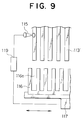
- Fig. 9 is an explanatory drawing of the relation between the focal position of a laser and the housing section of a wafer cassette.
- Fig. 10A and 10B are perspective views showing the conventional adhesion state of a semiconductor ingot and a disposable board, where Fig. 10A shows the state before slice and Fig. 10B shows the state after slice.
- Hereinafter, one embodiment of the present invention will be described by referring to the drawings.
- As shown in Fig. 3, a multi-wire saw according to this embodiment is provided with three wire guides 20, 21 and 22. In these wire guides, grooves corresponding to the thickness of the wafer to be sliced, the diameter of a wire and the like are cut and
wires 23 are wound along these grooves at a pitch of 600 µm. Thesewires 23 are travelled by a wire drive not shown. - Between the wire guides 21 and 22, two sets of
clip boards crystalline silicon block 24 therebetween are disposed movable on a wall free to ascend and descend 28 (cf. Figs. 4A to 4D). Incidentally, theclip boards silicon block 24 so as to keep thesilicon block 24 from being damaged. Furthermore, near the wire guides 21 and 22 are disposedslurry nozzles - In addition, a multi-wire saw is provided with a
cassette 5 as shown in Fig. 1A for housing a wafer sliced as it is. As material of a cassette, Teflon resin is used. In the 190 × 110 × 10 mmboards boards boards like boards - In a hole bored on the
boards wire 4 is spanned as partition. A 70 µm-diametered tungsten wire is used forwire 4. - A cassette may be arranged as shown in Fig. 2A. In Fig. 2A, the
cassette 6 comprisesside boards SUS round bars side boards round bars round bars round bars boards round bars wires 13 serving as partitions are disposed over a width of 70 mm from the center to the right and the left, that is, total width of 140 mm at a pitch of 600 µm. - Next, the operation of this embodiment will be described by referring to Figs. 4A to 4D and 5. Incidentally, with this embodiment, both ends of a 160 mm long semiconductor block is left untouched by 10 mm, respectively and accordingly the actual slice width is 140 mm.
- First, as shown in Fig. 4A, the
clip boards semiconductor block 24 therebetween. In this state, when a multi-wire saw starts, thewire 23 travels and simultaneously slurry jets from theslurry nozzles wall 28 is lowered by a not shown lift mechanism and consequently theclip boards semiconductor block 24 with thewire 23 is accomplished as shown in Fig. 4B. Incidentally, because the width of theclip boards semiconductor block 24 goes on the order of 55 mm and thewire 23 comes near theclip boards clip boards semiconductor block 24 therebetween as shown in Fig. 4C. At this time, the lower end of thesemiconductor block 24 is kept exposed on the order of 2 mm from the bottom of theclip boards semiconductor block 24 with theclip boards clip boards semiconductor block 24. - Meanwhile, because the clipping force of the
clip boards wafer 7 and the both 10 mm end portions of theblock 24, no breakage of a wafer occurs. The thickness of a wafer can be set at 200 to 450 µm and the cutting off ranges from 210 to 220 µm. - At the termination of slice, as shown in Fig. 4D, the
wafer 7 is held betweenclip boards clip boards top wires 4 of thecassette 5 are inserted into the respective gaps between a plurality ofwafers 7 and each wafer is held between theclip boards clip boards clip boards relevant wires 4 serving as partitions of thecassette 5 into thecassette 5, and when the half length of eachwafer 7 is housed in thecassette 5, the hold between theclip boards individual wafers 7 are housed into thecassette 5 while separated by thewires 4 serving as partitions of thecassette 5. - Incidentally, since slurry happens to gather between the
respective wafers 7 and consequently their sticking together is highly probable, it is advisable that theclip boards wafers 7 easily fall into thecassette 5. - With the multi-wire saw, wafers can be housed into the cassette as they are simultaneously to the completion of cutting and a very laborious work of manually tearing off a wafer hardly separable due to the residual slurry can be omitted. In addition, because of need for neither disposable board nor adhesive, the steps of applying and tearing off the adhesive can be omitted, thereby facilitating the operation greatly, and further the expendables, such as adhesive and disposable boards, can be saved, thereby enabling a cost cut.
- Hereinafter, another embodiment of the present invention will be described by referring to the drawings.
- Fig. 6 is a perspective view of a multi-wire saw device according to another embodiment of the present invention. Figs. 7A and 7B are perspective views showing an adhesion state of a semiconductor ingot and a disposable board, where Fig. 7A shows the state before slice by wires and Fig. 7B shows the state after slice.
- As shown in Fig. 6, the relevant multi-wire saw device comprises
wires 111, awire guide 112 for tensely spanning thewires 111 at predetermined spaces, adisposable board 114 fastened to a base plate to be mounted in the MWS device for fixing asemiconductor ingot block 113, aCO₂ laser 115 for cutting saidsemiconductor ingot block 113 at a right angle to the cutting direction of saidwire 111 and awafer cassette 116 for housing semiconductor wafers 113' after cutting. In Fig. 6,Numeral 117 denotes a travelling wafer cassette stand. - Said
wires 111, as one example, 180 µm in diameter, travel by wire driving mechanism not shown. - Said
wire guide 112 comprises, e.g., three wire guides, and these are provided with a plurality of grooves depending on the thickness of the semiconductor wafer 113' to be sliced, the diameter of saidwires 111 and the like, with which grooves saidwires 111 are spanned at predetermined spaces. Incidentally, only two wire guides are shown in Fig. 6. - Said
semiconductor ingot block 113, made of a crystalline silicon, whose wafer cut surface is 110 mm in long side and 100 mm in short side, comprises a parallelepiped, 160 mm long. - Said
disposable board 114, made, e.g., of glass board, carbon board or the like, is adhered and fixed throughadhesives 118 at one short side of thesemiconductor ingot block 113. - The
disposable board 114 is fixed to the base plate mounted through adhesive and a metal plate such as aluminum or a carbon board in the MWS device. Said base plate and said metal plate or carbon board are fastened with vises, or by inserting both ends of said metal plate or carbon board into said base plate. - Said
CO₂ laser 115, e.g., 500W in output power and 2500 mm/min in cutting rate, with the assist gas of Air, and disposed movable vertically, longitudinally and transversely, sets the length of a semiconductor wafer 113' on the long side of a wafer cut surface of asemiconductor ingot block 113 by the vertical movement, cuts the semiconductor wafer 113' by the transverse movement and aligns the focal position of theCO₂ laser 115 to the semiconductor wafer 113' to be cut by the longitudinal movement. - Said
wafer cassette 116 includes housing sections for individually housing a semiconductor wafer 113' after cutting and, for example, comprises as many housing sections as the number of semiconductor wafers 113' to be cut. - Hereinafter, a slice method of said
semiconductor ingot block 113 will be concretely described. - When slicing the
semiconductor ingot block 113 into a semiconductor wafer 113', first, fix a metal plate such as aluminum or a carbon board on the base plate mounted in the MWS device with vises or by inserting both ends into the base plate. - Next, bond a
disposable board 114 of glass or carbon board to said metal plate with adhesive, apply and harden adhesive 118 between saiddisposable board 114 and asemiconductor ingot block 113 at 50°C for 2 hours for bonding together. - And, mount this set ingot holder in the MWS device and start slicing while applying slurry, a mixture of whetstone grains and oil, over both ends. Here, conditions for slicing are let to be as follows: 6m/sec in the travelling rate of a wire, 300 µm in the lowering speed of a
semiconductor ingot block 113, and 350 µm in board thickness of the semiconductor wafer 113' to be sliced. - Slice proceeds and the
wire 111 enters the semiconductor ingot block by 105 mm to 107 mm, when the travelling of the wire and the lowering of thesemiconductor ingot block 113 stops. - Next, move the
CO₂ laser 115 to a predetermined position, that is, vertically move theCO₂ laser 115 in such a manner that the four sides of the wafer cut surface is equal in length (a semiconductor wafer of 100 mm × 100 mm), transversely move it in such a manner as to be positioned on either the left or right side with which a cut starts, and longitudinally move to adjust the focal position relative to the semiconductor wafer to be cut. As shown in Fig. 8, after aligning the position of theCO₂ laser 115 for each semiconductor wafer 113', cut individual semiconductor wafers 113' one by one. - As shown in Figs. 8A and 8B, the relevant cut semiconductor wafer 113' is housed in the
wafer cassette 116 provided below the semiconductor ingot block 113 (semiconductor wafer 113'). - Here, in each individual of said cut semiconductor wafer 113', a variation in thickness, e.g., a variation of 350 µm ± 10 µm occurs.
- Accordingly, as shown in Fig. 9, by having control means 119 for controlling the focal position of the
CO₂ laser 115 corresponding to the semiconductor wafer 113' to be cut and the position of the housing area start surface in saidhousing section 116a for housing the relevant semiconductor wafer 113' to come into much the same plane, for example, electrically sensing the focal position of theCO₂ laser 115 corresponding to the semiconductor wafer 113' to be cut and the position of thehousing section 116a corresponding to the relevant semiconductor wafer 113' and mechanically moving therelevant housing section 116a in synchronization with this sensing, all semiconductor 113' wafers can be stably housed inindividual housing sections 116a of the wafer cassette even if a variation occurs in the thickness of semiconductor wafers 113'. Thus, mistake in housing, damage of semiconductor wafers 113' or the like can be prevented. To be concrete, by a fine adjustment of the travellingwafer cassette stand 117, adjust the position of therelevant housing section 116a. - As described above, with the multi-wire saw device of this embodiment, because of being arranged to comprise a
laser 115 for cutting saidsemiconductor ingot block 113 at a right angle to the cutting direction of awire 111, saidsemiconductor ingot block 113 can be cut and separated by using awire 111 out of a row of wires and thelaser 115. This makes it unnecessary to slice even thedisposable board 114 with awire 111. Thus, semiconductor wafers 113' can be obtained without use of adisposable board 114 or without waste because a disposable board can be recycled even if used and consequently a cost cut in materials can be achieved. Furthermore, separating a semiconductor wafer 113' from thedisposable board 114 without use of solvent or the like becomes possible, thereby enhancing the operational efficiency. - By having a
wafer cassette 116 provided for housing a semiconductor wafer 113' to fall under saidsemiconductor ingot block 113 after the completion of cutting, semiconductor wafers 113' after cutting are automatically housed in thewafer cassette 116, so that it becomes possible to omit the very laborious operation of manually separating semiconductor wafers hardly separable due to the residual slurry from each other, thereby enabling an increase in yield and operational efficiency. - By incorporating a
housing sections 116a for individually housing individual semiconductor wafers 113' into saidwafer cassette 116 and having control means 119 provided for controlling the focal position of theCO₂ laser 115 corresponding to the semiconductor wafer 113' to be cut and the position of the housing area start surface in saidhousing sections 116a for housing the relevant semiconductor wafer 113' to come into much the same plane, said semiconductor wafers 113' can be stably housed in thehousing sections 116a of thewafer cassette 116 even if a variation occurs in the thickness of cut semiconductor wafers 113'. - With the slice method according to the present invention, because the wafer cut surface of said
semiconductor ingot block 113 comprises a rectangle and this method is arranged to comprise the steps of fixing the short side of saidsemiconductor ingot block 113 on said hold means; half-slicing saidsemiconductor ingot block 113 in the range from the short side up to the long side of the cut surface thereof; and cutting the semiconductor wafer after cutting in such a manner the wafer cut surface becomes a square by means of said laser, semiconductor wafers whose cut surface after cutting is a square can be obtained as ever without use of adisposable board 114 or without waste because a disposable board can be recycled if used. - Incidentally, a multi-wire saw device is described by using a parallelepiped of semiconductor ingot block in this embodiment, but needless to say, even if using a semiconductor ingot block having a partially flat cut surface in the width direction and held at the relevant cut surface by hold means, an equal advantage can be obtained.
- As described above, with a multi-wire saw device according to the present invention, because of being arranged to comprise a laser for cutting said semiconductor ingot at a right angle to the cutting direction of said wire, it is possible to cut said semiconductor ingot into individual wafers by using a row of wires and the laser and separate them from each other. Thus, it becomes unnecessary to slice even the hold means by means of wires and moreover no disposable board as a part of the hold means is used or a disposable board can be recycled even if used, so that semiconductor wafers can be obtained without waste and a cost cut in materials can be achieved. Furthermore, separating a semiconductor wafer from the hold means without use of solvent or the like becomes possible, thereby enhancing the operational efficiency.
- By having a wafer cassette provided for housing a semiconductor wafer to fall under said semiconductor ingot after the completion of cutting, semiconductor wafers after cutting are automatically housed in the wafer cassette, so that it becomes possible to omit the very laborious operation of manually separating semiconductor wafers hardly separable due to the residual slurry from each other, thereby enabling an increase in yield and operational efficiency.
- By incorporating a housing section for individually housing each individual semiconductor wafer into said wafer cassette and having control means provided for controlling the focal position of the laser on the semiconductor wafer to be cut and the position of the housing area start surface in said housing section for housing the relevant semiconductor wafer to come into much the same plane, said semiconductor wafers can be stably housed in the housing section of the wafer cassette even if a variation occurs in the thickness of cut semiconductor wafers.
- With the slice method according to the present invention, because the wafer cut surface of said semiconductor ingot comprises a rectangle and this method is arranged to comprise the steps of fixing the short side of said semiconductor ingot on said hold means; half-slicing said semiconductor ingot in the range from the short side up to the long side of the cut surface thereof; and cutting the semiconductor wafer after cutting in such a manner the wafer cut surface becomes a square by means of said laser, semiconductor wafers whose cut surface after cutting is a square can be obtained as ever without use of a disposable board as a part of said hold means or without wasting a disposable board if used.
- Many widely different embodiments of the present invention may be constructed without departing from the spirit and scope of the present invention. It should be understood that the present invention is not limited to the specific embodiments described in the specification, except as defined in the appended claims.
Claims (8)
- A multi-wire saw for cutting a semiconductor ingot into plenty of wafer by using a row of wires (23) spanned at predetermined spaces, characterized by comprising hold means (25a, 25b, 26a, 26b) for holding said semiconductor ingot therein and moving it at a right angle to the travelling direction of said wires for cutting it into wafers, wherein it is arranged to let a wafer fall from said hold means into a wafer housing cassette (6) after the completion of cutting.
- The multi-wire saw as set forth in Claim 1, characterized in that said hold means comprises a first sandwich holding section (25a, 25b) for holding a semiconductor ingot therein at the first half of the cutting step and a second sandwich holding section (26a, 26b) for holding said semiconductor ingot therein at the second half of the cutting step.
- A wafer housing cassette (6) used with the multi-wire saw as set forth in Claim 1, characterized in that wires, 50 to 300 µm in diameter, are spanned as partitions for separating wafers from each other.
- A multi-wire saw device for cutting a semiconductor ingot into plenty of conductor wafer by using a row of wires (111) tensely arranged at predetermined spaces, characterized by comprising hold means (114) for holding said semiconductor ingot and a laser (115) for cutting said semiconductor ingot at a right angle to the cutting direction of said wires.
- The multi-wire saw device as set forth in Claim 4, characterized in that said laser is arranged to be movable vertically, longitudinally and transversely.
- The multi-wire saw device as set forth in Claim 4, characterized by further comprising a wafer cassette (116) for housing a semiconductor wafer to fall under said semiconductor ingot after the completion of cutting.
- The multi-wire saw device as set forth in Claim 6, characterized in that said wafer cassette (116) includes housing sections (116a) for individually housing individual semiconductor wafers and further comprises control means (119) for controlling the focal position of the laser on the semiconductor wafer to be cut and the position of the housing area start surface in said housing section for housing the relevant semiconductor wafer to come into much the same plane.
- A slice method using the multi-wire saw device as set forth in Claim 4 characterized in that the wafer cut surface of said semiconductor ingot comprises a rectangle, comprising the steps of fixing the short side of said semiconductor ingot on said hold means; half-slicing said semiconductor ingot in the range from the short side up to the long side of the cut surface thereof; and cutting the semiconductor wafer after cutting in such a manner the wafer cut surface becomes a square by means of said laser.
Applications Claiming Priority (6)
| Application Number | Priority Date | Filing Date | Title |
|---|---|---|---|
| JP31162494A JP3143570B2 (en) | 1994-12-15 | 1994-12-15 | Multi wire saw |
| JP31162494 | 1994-12-15 | ||
| JP311624/94 | 1994-12-15 | ||
| JP06812595A JP3163231B2 (en) | 1995-03-27 | 1995-03-27 | Multi-wire saw device and slicing method using the same |
| JP68125/95 | 1995-03-27 | ||
| JP6812595 | 1995-03-27 |
Publications (3)
| Publication Number | Publication Date |
|---|---|
| EP0716910A2 true EP0716910A2 (en) | 1996-06-19 |
| EP0716910A3 EP0716910A3 (en) | 1997-05-02 |
| EP0716910B1 EP0716910B1 (en) | 2002-03-27 |
Family
ID=26409358
Family Applications (1)
| Application Number | Title | Priority Date | Filing Date |
|---|---|---|---|
| EP95119709A Expired - Lifetime EP0716910B1 (en) | 1994-12-15 | 1995-12-14 | Multi-wire saw device and slice method using the same |
Country Status (3)
| Country | Link |
|---|---|
| US (1) | US5715806A (en) |
| EP (1) | EP0716910B1 (en) |
| DE (1) | DE69526038T2 (en) |
Cited By (3)
| Publication number | Priority date | Publication date | Assignee | Title |
|---|---|---|---|---|
| EP1555101A1 (en) * | 2003-12-17 | 2005-07-20 | HCT Shaping Systems SA | Wire saw device |
| DE102007028439A1 (en) | 2007-06-18 | 2008-12-24 | Schott Ag | Separating flat-parallel silicon wafers from cuboid crystalline or polycrystalline silicon ingot using wire saw for photo-voltaic applications, comprises moving wire around rolls, and attaching the ingot to reception of the wire saw |
| CN113752402A (en) * | 2021-09-16 | 2021-12-07 | 广东金湾高景太阳能科技有限公司 | Method for solving scratch bright line of large-size silicon wafer lifting material |
Families Citing this family (34)
| Publication number | Priority date | Publication date | Assignee | Title |
|---|---|---|---|---|
| CZ283541B6 (en) * | 1996-03-06 | 1998-04-15 | Trimex Tesla, S.R.O. | Process of cutting ingots from hard materials to plates and a saw for making the same |
| JPH09272119A (en) * | 1996-04-04 | 1997-10-21 | Daido Hoxan Inc | Wafer manufacturing method and apparatus used therefor |
| JPH09286021A (en) * | 1996-04-22 | 1997-11-04 | Komatsu Electron Metals Co Ltd | Cutting method of semiconductor ingot |
| JPH1022244A (en) * | 1996-06-29 | 1998-01-23 | Komatsu Electron Metals Co Ltd | Cleaning basket for semiconductor wafers |
| JP3273163B2 (en) * | 1996-09-06 | 2002-04-08 | シャープ株式会社 | Multi wire saw |
| US5878737A (en) * | 1997-07-07 | 1999-03-09 | Laser Technology West Limited | Apparatus and method for slicing a workpiece utilizing a diamond impregnated wire |
| WO1999002295A2 (en) * | 1997-07-07 | 1999-01-21 | Laser Technology West, Limited | Apparatus and method for slicing a workpiece utilizing a diamond impregnated wire |
| US6024080A (en) * | 1997-07-07 | 2000-02-15 | Laser Technology West Limited | Apparatus and method for slicing a workpiece utilizing a diamond impregnated wire |
| US6279564B1 (en) | 1997-07-07 | 2001-08-28 | John B. Hodsden | Rocking apparatus and method for slicing a workpiece utilizing a diamond impregnated wire |
| JP3625408B2 (en) * | 1999-03-09 | 2005-03-02 | シャープ株式会社 | Machining method using multi-wire saw |
| US6112738A (en) * | 1999-04-02 | 2000-09-05 | Memc Electronics Materials, Inc. | Method of slicing silicon wafers for laser marking |
| US6915796B2 (en) * | 2002-09-24 | 2005-07-12 | Chien-Min Sung | Superabrasive wire saw and associated methods of manufacture |
| CH696807A5 (en) * | 2003-01-13 | 2007-12-14 | Hct Shaping Systems S A | Wire sawing device. |
| KR20070004073A (en) * | 2004-03-30 | 2007-01-05 | 솔라익스 인코퍼레이티드 | Ultra-thin silicon wafer cutting method and apparatus |
| KR100667690B1 (en) | 2004-11-23 | 2007-01-12 | 주식회사 실트론 | Wafer Slicing Method and Apparatus |
| DE102005028112A1 (en) * | 2005-06-13 | 2006-12-21 | Schmid Technology Systems Gmbh | Method for positioning and maintaining the position of substrates, in particular of thin silicon wafers after wire sawing for their separation |
| DE102006050330B4 (en) * | 2006-10-25 | 2009-10-22 | Siltronic Ag | A method for simultaneously separating at least two cylindrical workpieces into a plurality of slices |
| US20090060821A1 (en) * | 2007-08-27 | 2009-03-05 | Andreas Menzel | Method for manufacturing silicone wafers |
| US20100300259A1 (en) * | 2009-05-29 | 2010-12-02 | Applied Materials, Inc. | Substrate side marking and identification |
| EP2477777A1 (en) * | 2009-09-18 | 2012-07-25 | Applied Materials, Inc. | Wire saw work piece support device, support spacer and method of sawing using same |
| TW201112317A (en) * | 2009-09-22 | 2011-04-01 | Ching Hung Machinery & Electric Ind Co Ltd | Serial multi-thread saw crystal slicing device |
| CN102172996B (en) * | 2011-02-14 | 2014-09-24 | 上海日进机床有限公司 | Crystal immersing and cutting method |
| JP2013038116A (en) * | 2011-08-04 | 2013-02-21 | Sumitomo Electric Ind Ltd | Manufacturing method of group iii nitride crystal substrate |
| DE102011090053A1 (en) * | 2011-12-28 | 2013-07-04 | Robert Bosch Gmbh | Separation device and method for separating a metallic or ceramic blank |
| US20130251940A1 (en) * | 2012-03-23 | 2013-09-26 | Sheng Sun | Method of cutting an ingot for solar cell fabrication |
| US20150053650A1 (en) * | 2012-04-12 | 2015-02-26 | Mitsubishi Electric Corporation | Wire discharge machining apparatus and manufacturing method for semiconductor wafers using the same |
| CN102941628B (en) * | 2012-07-31 | 2014-12-24 | 南通皋鑫电子股份有限公司 | Diode silicon stack cutting process and special tool thereof |
| CN103878891A (en) * | 2012-12-24 | 2014-06-25 | 九州方园新能源股份有限公司 | Silicon rod with chamfered guide strip |
| DE102013202028A1 (en) * | 2013-02-07 | 2014-08-07 | Robert Bosch Gmbh | Method for producing wafers, in particular wafers for solar cells, and apparatus for producing wafers |
| CN105216127B (en) * | 2015-08-28 | 2017-07-07 | 厦门钨业股份有限公司 | Multi-line cutting method and multi-line cutting machine |
| JP6249319B1 (en) * | 2017-03-30 | 2017-12-20 | パナソニックIpマネジメント株式会社 | Saw wire and cutting device |
| CN108638353A (en) * | 2017-05-24 | 2018-10-12 | 林晓丽 | Utilize the equipment of Buddha's warrior attendant wire cutting |
| JP6751900B2 (en) * | 2018-01-29 | 2020-09-09 | パナソニックIpマネジメント株式会社 | Metal wire and saw wire |
| CN111361030B (en) * | 2020-04-24 | 2021-11-23 | 西安奕斯伟材料科技有限公司 | Multi-wire cutting device and multi-wire cutting method |
Family Cites Families (16)
| Publication number | Priority date | Publication date | Assignee | Title |
|---|---|---|---|---|
| US1619128A (en) * | 1923-12-17 | 1927-03-01 | Uline Ice Scoring Machine Comp | Ice-scoring machine |
| US2024715A (en) * | 1934-11-21 | 1935-12-17 | William C Bonnett | Apparatus for making button blanks from pearl stock |
| US3032026A (en) * | 1959-07-18 | 1962-05-01 | Bosch Gmbh Robert | Device for slicing semiconductor crystals and the like |
| US3540427A (en) * | 1968-06-14 | 1970-11-17 | Ibm | Electro-optic array and method of making same |
| US3599623A (en) * | 1969-09-02 | 1971-08-17 | Fairchild Camera Instr Co | Cutting apparatus for making finely controlled cuts utilizing a tiltable wheel for regulating the cutting blade movement |
| SU715345A1 (en) * | 1977-11-02 | 1980-02-15 | Всесоюзный Научно-Исследовательский И Проектно-Изыскательский Институт По Проблемам Добычи Транспорта И Переработки Минерального Сырья В Промышленности Строительных Материалов | Method of making curbstones |
| US4287869A (en) * | 1978-03-13 | 1981-09-08 | Crystal Systems Inc. | Charging system for cutting blade |
| US4625093A (en) * | 1984-08-14 | 1986-11-25 | Massachusetts Institute Of Technology | Stock removal by laser cutting |
| JPS61182761A (en) * | 1985-02-07 | 1986-08-15 | Sumitomo Metal Ind Ltd | Wafer take out method of wire saw |
| US4655191A (en) * | 1985-03-08 | 1987-04-07 | Motorola, Inc. | Wire saw machine |
| JP2673544B2 (en) * | 1988-06-14 | 1997-11-05 | 株式会社日平トヤマ | Cutting method for brittle materials |
| US5054626A (en) * | 1990-09-13 | 1991-10-08 | George Stempinski | Storage rack |
| JPH0790547B2 (en) * | 1990-11-01 | 1995-10-04 | 住友金属工業株式会社 | Cutting method with multi-wire saw |
| JP2551229B2 (en) * | 1990-11-01 | 1996-11-06 | 住友金属工業株式会社 | Cutting method and apparatus using multi-wire saw |
| DE4134110A1 (en) * | 1991-10-15 | 1993-04-22 | Wacker Chemitronic | METHOD FOR ROTARY SAWING OF SPROEDHARD MATERIALS, ESPECIALLY SUCH WITH DIAMETERS OVER 200 MM IN THIN DISC MEDIA BY MEANS OF INSIDE HOLE SAW, AND DEVICE FOR CARRYING OUT THE METHOD |
| JP3325676B2 (en) * | 1993-11-29 | 2002-09-17 | シャープ株式会社 | Slicing method of silicon ingot |
-
1995
- 1995-12-14 DE DE69526038T patent/DE69526038T2/en not_active Expired - Lifetime
- 1995-12-14 EP EP95119709A patent/EP0716910B1/en not_active Expired - Lifetime
- 1995-12-14 US US08/572,608 patent/US5715806A/en not_active Expired - Lifetime
Non-Patent Citations (1)
| Title |
|---|
| None |
Cited By (5)
| Publication number | Priority date | Publication date | Assignee | Title |
|---|---|---|---|---|
| EP1555101A1 (en) * | 2003-12-17 | 2005-07-20 | HCT Shaping Systems SA | Wire saw device |
| DE102007028439A1 (en) | 2007-06-18 | 2008-12-24 | Schott Ag | Separating flat-parallel silicon wafers from cuboid crystalline or polycrystalline silicon ingot using wire saw for photo-voltaic applications, comprises moving wire around rolls, and attaching the ingot to reception of the wire saw |
| CN113752402A (en) * | 2021-09-16 | 2021-12-07 | 广东金湾高景太阳能科技有限公司 | Method for solving scratch bright line of large-size silicon wafer lifting material |
| CN113752402B (en) * | 2021-09-16 | 2022-07-12 | 广东金湾高景太阳能科技有限公司 | A solution for large-size silicon wafers to scratch bright lines |
| US12275164B2 (en) | 2021-09-16 | 2025-04-15 | Guangdong Jinwan Gokin Solar Technology Co., Ltd | Method for solving bright line scratched during lifting of large-size silicon wafer |
Also Published As
| Publication number | Publication date |
|---|---|
| EP0716910B1 (en) | 2002-03-27 |
| EP0716910A3 (en) | 1997-05-02 |
| DE69526038D1 (en) | 2002-05-02 |
| US5715806A (en) | 1998-02-10 |
| DE69526038T2 (en) | 2002-10-31 |
Similar Documents
| Publication | Publication Date | Title |
|---|---|---|
| EP0716910B1 (en) | Multi-wire saw device and slice method using the same | |
| US4227348A (en) | Method of slicing a wafer | |
| US20070131213A1 (en) | Cutting method by wire saw and cut workpiece receiving member in wire saw | |
| EP0376514A2 (en) | Method of fabricating large array semiconductor devices | |
| JP3745016B2 (en) | Replaceable semiconductor chip | |
| US4184472A (en) | Method and apparatus for slicing crystals | |
| CN115519236B (en) | Laser processing device and method for connecting plate for tunnel support steel arch | |
| KR20080076711A (en) | Method and apparatus for separating laminated glass sheet | |
| US6119673A (en) | Wafer retrieval method in multiple slicing wire saw | |
| CN101356047A (en) | Apparatus and method for separating and transporting substrates | |
| JPH04503284A (en) | Separation of diode array chip during fabrication of diode array chip | |
| JP3163231B2 (en) | Multi-wire saw device and slicing method using the same | |
| US5706176A (en) | Butted chip array with beveled chips | |
| JP3143570B2 (en) | Multi wire saw | |
| US4287256A (en) | Wafer and boule protection during the blade return stroke of a wafer saw | |
| JP4116509B2 (en) | Tape member sticking device | |
| JPH0550422A (en) | Cutting method by means of multiwire saw | |
| WO1998052212A1 (en) | Pick and place cutting head that separates chip scale packages from a multi-layered film strip | |
| JPS6298684A (en) | Cleavage device and method | |
| JP2551229B2 (en) | Cutting method and apparatus using multi-wire saw | |
| JP3716555B2 (en) | Multi-cut wire saw work cutting method | |
| JP2000294521A (en) | Manufacturing method of electronic element | |
| JP2714556B2 (en) | Circuit board dividing mold driving method and circuit board dividing apparatus | |
| CN215750096U (en) | Cutting mechanism and cutting equipment | |
| CN222290601U (en) | A stone wire saw cutting machine |
Legal Events
| Date | Code | Title | Description |
|---|---|---|---|
| PUAI | Public reference made under article 153(3) epc to a published international application that has entered the european phase |
Free format text: ORIGINAL CODE: 0009012 |
|
| AK | Designated contracting states |
Kind code of ref document: A2 Designated state(s): CH DE FR LI |
|
| PUAL | Search report despatched |
Free format text: ORIGINAL CODE: 0009013 |
|
| AK | Designated contracting states |
Kind code of ref document: A3 Designated state(s): CH DE FR LI |
|
| 17P | Request for examination filed |
Effective date: 19970709 |
|
| 17Q | First examination report despatched |
Effective date: 20000228 |
|
| GRAG | Despatch of communication of intention to grant |
Free format text: ORIGINAL CODE: EPIDOS AGRA |
|
| RTI1 | Title (correction) |
Free format text: MULTI-WIRE SAW DEVICE AND SLICE METHOD USING THE SAME |
|
| GRAG | Despatch of communication of intention to grant |
Free format text: ORIGINAL CODE: EPIDOS AGRA |
|
| GRAH | Despatch of communication of intention to grant a patent |
Free format text: ORIGINAL CODE: EPIDOS IGRA |
|
| GRAH | Despatch of communication of intention to grant a patent |
Free format text: ORIGINAL CODE: EPIDOS IGRA |
|
| GRAA | (expected) grant |
Free format text: ORIGINAL CODE: 0009210 |
|
| AK | Designated contracting states |
Kind code of ref document: B1 Designated state(s): CH DE FR LI |
|
| REG | Reference to a national code |
Ref country code: CH Ref legal event code: NV Representative=s name: E. BLUM & CO. PATENTANWAELTE Ref country code: CH Ref legal event code: EP |
|
| REF | Corresponds to: |
Ref document number: 69526038 Country of ref document: DE Date of ref document: 20020502 |
|
| ET | Fr: translation filed | ||
| PLBE | No opposition filed within time limit |
Free format text: ORIGINAL CODE: 0009261 |
|
| STAA | Information on the status of an ep patent application or granted ep patent |
Free format text: STATUS: NO OPPOSITION FILED WITHIN TIME LIMIT |
|
| 26N | No opposition filed |
Effective date: 20021230 |
|
| REG | Reference to a national code |
Ref country code: CH Ref legal event code: PFA Owner name: SHARP KABUSHIKI KAISHA Free format text: SHARP KABUSHIKI KAISHA#22-22 NAGAIKE-CHO, ABENO-KU#OSAKA-SHI, OSAKA-FU 545-0013 (JP) -TRANSFER TO- SHARP KABUSHIKI KAISHA#22-22 NAGAIKE-CHO, ABENO-KU#OSAKA-SHI, OSAKA-FU 545-0013 (JP) |
|
| PGFP | Annual fee paid to national office [announced via postgrant information from national office to epo] |
Ref country code: CH Payment date: 20121213 Year of fee payment: 18 Ref country code: DE Payment date: 20121213 Year of fee payment: 18 |
|
| PGFP | Annual fee paid to national office [announced via postgrant information from national office to epo] |
Ref country code: FR Payment date: 20130107 Year of fee payment: 18 |
|
| REG | Reference to a national code |
Ref country code: DE Ref legal event code: R119 Ref document number: 69526038 Country of ref document: DE |
|
| REG | Reference to a national code |
Ref country code: CH Ref legal event code: PL |
|
| REG | Reference to a national code |
Ref country code: FR Ref legal event code: ST Effective date: 20140829 |
|
| REG | Reference to a national code |
Ref country code: DE Ref legal event code: R119 Ref document number: 69526038 Country of ref document: DE Effective date: 20140701 |
|
| PG25 | Lapsed in a contracting state [announced via postgrant information from national office to epo] |
Ref country code: CH Free format text: LAPSE BECAUSE OF NON-PAYMENT OF DUE FEES Effective date: 20131231 Ref country code: DE Free format text: LAPSE BECAUSE OF NON-PAYMENT OF DUE FEES Effective date: 20140701 Ref country code: LI Free format text: LAPSE BECAUSE OF NON-PAYMENT OF DUE FEES Effective date: 20131231 |
|
| PG25 | Lapsed in a contracting state [announced via postgrant information from national office to epo] |
Ref country code: FR Free format text: LAPSE BECAUSE OF NON-PAYMENT OF DUE FEES Effective date: 20131231 |