EP0725443A1 - Dispositif semi-conducteur - Google Patents
Dispositif semi-conducteur Download PDFInfo
- Publication number
- EP0725443A1 EP0725443A1 EP96300501A EP96300501A EP0725443A1 EP 0725443 A1 EP0725443 A1 EP 0725443A1 EP 96300501 A EP96300501 A EP 96300501A EP 96300501 A EP96300501 A EP 96300501A EP 0725443 A1 EP0725443 A1 EP 0725443A1
- Authority
- EP
- European Patent Office
- Prior art keywords
- insulating gate
- conductivity channel
- nmos
- signal
- circuit
- Prior art date
- Legal status (The legal status is an assumption and is not a legal conclusion. Google has not performed a legal analysis and makes no representation as to the accuracy of the status listed.)
- Granted
Links
Images


Classifications
-
- H—ELECTRICITY
- H10—SEMICONDUCTOR DEVICES; ELECTRIC SOLID-STATE DEVICES NOT OTHERWISE PROVIDED FOR
- H10D—INORGANIC ELECTRIC SEMICONDUCTOR DEVICES
- H10D84/00—Integrated devices formed in or on semiconductor substrates that comprise only semiconducting layers, e.g. on Si wafers or on GaAs-on-Si wafers
- H10D84/80—Integrated devices formed in or on semiconductor substrates that comprise only semiconducting layers, e.g. on Si wafers or on GaAs-on-Si wafers characterised by the integration of at least one component covered by groups H10D12/00 or H10D30/00, e.g. integration of IGFETs
- H10D84/82—Integrated devices formed in or on semiconductor substrates that comprise only semiconducting layers, e.g. on Si wafers or on GaAs-on-Si wafers characterised by the integration of at least one component covered by groups H10D12/00 or H10D30/00, e.g. integration of IGFETs of only field-effect components
- H10D84/83—Integrated devices formed in or on semiconductor substrates that comprise only semiconducting layers, e.g. on Si wafers or on GaAs-on-Si wafers characterised by the integration of at least one component covered by groups H10D12/00 or H10D30/00, e.g. integration of IGFETs of only field-effect components of only insulated-gate FETs [IGFET]
- H10D84/85—Complementary IGFETs, e.g. CMOS
-
- H—ELECTRICITY
- H10—SEMICONDUCTOR DEVICES; ELECTRIC SOLID-STATE DEVICES NOT OTHERWISE PROVIDED FOR
- H10D—INORGANIC ELECTRIC SEMICONDUCTOR DEVICES
- H10D86/00—Integrated devices formed in or on insulating or conducting substrates, e.g. formed in silicon-on-insulator [SOI] substrates or on stainless steel or glass substrates
- H10D86/201—Integrated devices formed in or on insulating or conducting substrates, e.g. formed in silicon-on-insulator [SOI] substrates or on stainless steel or glass substrates the substrates comprising an insulating layer on a semiconductor body, e.g. SOI
Definitions
- the present invention relates to a semiconductor device and, more particularly, to a semiconductor device (semiconductor integrated circuit apparatus) in which a signal input portion has an amplifying circuit including one or two or more insulating gate type transistors such as MOS transistors and which can process, especially, a micro signal.
- a semiconductor device semiconductor integrated circuit apparatus
- a signal input portion has an amplifying circuit including one or two or more insulating gate type transistors such as MOS transistors and which can process, especially, a micro signal.
- CMOS complementary metal-oxide-semiconductor
- a source of a P-channel MOS transistor (hereinbelow, referred to as a PMOS Tr) M1 is connected to a V DD power source terminal 100
- a drain of the PMOS Tr M1 is commonly connected to a drain of an N-channel MOS transistor (hereinbelow, referred to as an NMOS Tr) M2
- a source of the NMOS Tr M2 is connected to a ground terminal 101
- gates of the PMOS Tr M1 and NMOS Tr M2 are commonly connected to an input terminal 1
- a back gate of the PMOS Tr M1 is connected to the V DD power source terminal 100
- a back gate of the NMOS Tr M2 is connected to the ground terminal 101, thereby constructing a CMOS inverter.
- An output of the CMOS inverter constructed by the PMOS Tr M1 and NMOS Tr M2 is connected to an input of an internal circuit (a CMOS inverter constructed by a PMOS Tr M3 and an NMOS Tr M4 in a manner similar to the CMOS inverter constructed by the PMOS Tr M1 and NMOS Tr M2 in Fig. 1).
- the PMOS Tr M1 of the input inverter and the PMOS Tr M3 of the internal circuit are formed on a same N well 12 as shown in Fig. 2 and the NMOS Tr M2 of the input inverter and the NMOS Tr M4 of the internal circuit are formed on a P-type substrate 15.
- reference numeral 2001 denotes an n - region formed in the P-type substrate 15.
- the PMOS Trs M1 and M3 are formed in this n - region.
- Reference numerals 2002, 2003, 2004, and 2005 indicate p + regions formed in the n - region 2001, respectively.
- the p + region 2003 becomes a source region of the PMOS Tr M1
- the p + region 2005 becomes a source region of the PMOS Tr M3
- the p + region 2002 becomes a drain region of the PMOS Tr M1
- the p + region 2004 becomes a drain region of the PMOS Tr M3.
- Reference numerals 2007, 2008, 2009, and 2010 denote gate electrodes of the MOS Trs, respectively; 2006 and 2015 indicate back gates; and 2011, 2012, 2013, and 2014 show n + regions.
- the n + region 2011 becomes a source region of the NMOS Tr M2
- the n + region 2013 becomes a source region of the NMOS Tr M4
- the n + region 2012 becomes a drain region of the NMOS Tr M2
- the n + region 2014 becomes a drain region of the NMOS Tr M4.
- the back gate 2006 is set to an n + region in order to obtain a potential of the n - region 2001.
- the back gate 2015 is set to a p + region in order to obtain a potential of the P-type substrate 15.
- CMOS inverter when a signal of a micro amplitude is handled, it is important that a threshold level of the CMOS inverter and a DC level of an input signal coincide. In the case where the threshold level of the CMOS inverter is slightly deviated, there is a case where an erroneous operation of the circuit or the like occurs.
- the invention is made in consideration of the above problems and it is an object of the invention to provide a semiconductor device which prevents an erroneous operation of a circuit or the like due to a difference between a threshold level of a signal amplifying circuit and a DC level of a micro input signal.
- Another object of the invention is to provide a semiconductor device which can perform a correct operation even for a smaller micro signal.
- Still another object of the invention is to provide a semiconductor device in which a signal input portion is constructed by an amplifying circuit including one or two or more insulating gate type transistors, wherein one insulating gate type transistor or at least one of the two or more insulating gate type transistors of the signal input portion is an insulating gate type transistor of a first conductivity channel type and the insulating gate type transistor of the first conductivity channel type is formed in a semiconductor region that is electrically isolated from another insulating gate type transistor of the first conductivity channel type provided in a circuit portion other than the signal input portion.
- Another object of the invention is to provide a semiconductor device in which a signal input portion is constructed by an amplifying circuit including an insulating gate type transistor of a first conductivity channel type and an insulating gate type transistor of a second conductivity channel type different from the first conductivity channel type, wherein the insulating gate type transistor of the first conductivity channel type is formed in a semiconductor region that is electrically isolated from another insulating gate type transistor of the first conductivity channel type provided in a circuit portion other than the signal input portion.
- a semiconductor region of a signal input portion in which an insulating gate type transistor is formed is independently provided so as to be electrically isolated from an insulating gate type transistor of a same conductivity channel type provided in a circuit portion other than the signal input portion.
- Figs. 3 and 4 are a schematic circuit diagram and a schematic vertical sectional view each showing the first embodiment of the invention and show a case where the invention is applied to the circuit construction shown in Fig. 1.
- the same component elements as those in Fig. 1 are designated by the same reference numerals.
- reference numeral 100 denotes the power source terminal; 101 the ground terminal; 1 the signal input terminal; 200 an output terminal: M1 and M3 the PMOS transistors; and M2 and M4 the NMOS transistors.
- An input CMOS inverter circuit is constructed by the PMOS Tr M1 and NMOS Tr M2 and an internal CMOS inverter circuit is constructed by the PMOS Tr M3 and NMOS Tr M4, respectively.
- the PMOS Tr M1 is formed in an N well 10
- the PMOS Tr M3 is formed in an N well 12
- the NMOS Trs M2 and M4 are formed on the P-type substrate 15.
- the N well 10 is connected to a well potential control terminal 20 through a back gate 2006-1 as an n + region.
- the N well 12 is connected to the power source terminal 100 through the back gate 2006.
- the P-type substrate 15 is connected to the ground terminal 101 through the back gate 2015 as a p + region.
- ⁇ denotes a mobility of a carrier
- C OX an oxide film capacitance
- (W p /L p ) or (W n /L n ) a size of the PMOS Tr or the NMOS Tr
- W p and W n widths of the transistors
- V Tp T TOp + ⁇ ( 2 ⁇ f + V SBp - 2 ⁇ f )
- V Tn T TOn + ⁇ ( 2 ⁇ f + V SBn - 2 ⁇ f )
- V in V DD + V Tp + K n K p V Tn 1 + K n K p
- the well potential control terminal 20 in the first embodiment is means for controlling V SBp in the equation (5) and controls the threshold voltage of the CMOS inverter so as to coincide with a DC level of a micro input signal, so that the accurate operation can be realized. It is considered that the threshold voltage of the CMOS inverter which is expressed by the equation (7) changes due to variations in size of MOS Tr, process parameter, and the like. The well potential control terminal 20, however, can correct such variations.
- Figs. 5 and 6 show a case where the second embodiment of the invention is applied to the circuit construction shown in Fig. 1.
- the same component elements as those in Fig. 1 are designated by the same reference numerals (the same shall also similarly apply to embodiments which will be described hereinlater).
- a P well 11 in which the NMOS Tr M2 constructing the input CMOS inverter is formed and a P well 13 in which the NMOS Tr M4 in the internal circuit is formed are formed by using n + buried layers 2060-1 to 2060-4 so as to be electrically isolated.
- the P well 11 is connected to a well potential control terminal 21 through a p + region 2015-1.
- the P well 13 is connected to the ground terminal 101 through the p + region 2015. Therefore, as compared with the first embodiment in which only the well potential of the PMOS Tr M1 constructing the input CMOS inverter is controlled, the second embodiment is constructed in a manner such that the well potential of the NMOS Tr M2 can be also simultaneously controlled. With such a construction, the threshold voltage of the input CMOS inverter can be controlled in a wider range.
- reference numerals 2061-1 and 2061-2 denote p + regions, respectively.
- Figs. 7 and 8 show a case where the third embodiment of the invention is applied to the circuit construction shown in Fig. 1.
- the N wells 10 and 12 and the P wells 11 and 13 which are respectively electrically isolated are formed on an SOI substrate having an isolating layer 16 formed on a substrate 8001 such as a semiconductor substrate or the like
- the PMOS Tr M1 constructing the input CMOS inverter is formed on the N well 10
- the PMOS Tr M3 constructing the internal circuit is formed on the N well 12
- the NMOS Tr M2 constructing the input CMOS inverter
- the NMOS Tr M4 constructing the internal circuit is formed on the P well 13.
- the N wells 10 and 12 are connected to the well potential control terminal 20 and power source terminal 100, respectively.
- the P wells 11 and 13 are connected to the well potential control terminal 21 and ground terminal 101, respectively.
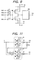
- Fig. 9 shows a circuit according to the forth embodiment of the invention.
- the embodiment shows a case where the invention is applied to a ⁇ -MOS circuit.
- reference numerals 9001, 9002, 9003, ..., 900n denote signal input terminals and C 1 , C 2 , C 3 , ..., C n indicate capacitors. Terminals on the side opposite to the signal input terminals of the capacitances are commonly connected to an input of the CMOS inverter constructed by the PMOS Tr M1 and NMOS Tr M2, respectively.
- Reference numeral 500 denotes an internal circuit connected to an output of the CMOS inverter; 200 the output terminal; and 20 and 21 the potential control terminals of the wells in which the PMOS Tr M1 and NMOS Tr M2 are formed, respectively.
- an input voltage amplitude of the CMOS inverter constructed by the PMOS Tr M1 and NMOS Tr M2 becomes as follows by assuming that voltages which are supplied to input terminals 1, 2, 3, ..., n are set to V 1 , V 2 , V 3 , ..., V n .
- the threshold voltage of the CMOS inverter is made coincide with the input DC level, thereby enabling the operation to be accurately performed.
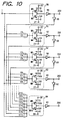
- Fig. 10 is a circuit diagram showing the fifth embodiment of the invention and shows an example of an 8-bit A/D (analog - digital) converter of a multi-step type constructed by using the foregoing ⁇ -MOS.
- reference numerals 50 to 54 denote CMOS inverters of the invention; 55 to 63 CMOS inverters; C 1 to C 17 the capacitors; 200 to 204 digital output terminals; and 1 the analog input terminal.
- the analog input terminal 1 is connected to an input of the inverter 50 and is also connected to inputs of the inverters 51, 52, 53, and 54 through the capacitors C 2 , C 5 , C 9 , and C 17 .
- An output of the inverter 50 is connected to the digital output terminal (MSB) 200 through the inverter 55 and is also connected to inputs of the inverters 51, 52, 53, and 54 through the capacitors C 1 , C 4 , C 8 , and C 16 .
- An output of the inverter 51 is connected to the digital output terminal 201 through the inverter 57 and is also connected to the inverter 52, 53, and 54 through the capacitors C 3 , C 7 , and C 15 .
- outputs of upper bits are sequentially connected to inputs of all of lower inverters through the inverters and capacitors.
- an analog signal inputted from the digital output terminal 200 is converted to a digital signal and is outputted.
- a voltage at an input point (a) of the inverter 51 is set to a value obtained by dividing a difference between the power source voltage and the voltage V 1 by a capacitance ratio of the capacitors C 1 and C 2 as follows by setting V 1 to a reference.
- V a V 1 + C 1 C 1 + C 2 (V DD - V 1 )
- V a V 1 + C 1 C 1 + C 2 (V DD - V 1 )
- a potential at the (a) point is set to the following value V a obtained by dividing V 1 by the capacitance ratio of C 1 and C 2 .
- V a C 2 C 1 + C 2 V 1 Since the value V a is smaller than the threshold value of the inverter 51, the signal of the inverter 51 is inverted, so that the output 201 is set to the low level.
- V 1 further increases, V a increases in proportion to the value V 1 .
- V a exceeds the threshold value of the inverter 51, the output 201 is inverted and is set to the high level (refer to Fig. 12).
- the capacitance dividing ratio decreases and the amplitude decreases. Since a parasitic gate capacitance exists in each of the MOS Trs M1 to M10 constructing the inverters 50 to 54, the voltage which is supplied to each of the inverters is deviated to the DC level by an offset voltage V OS as shown by V a ' in Fig. 12. In this case, a deviation occurs in the timing of the digital output as shown by a broken line V201 in Fig. 12, so that an erroneous operation is causes.
- the threshold value of each inverter is controlled so as to coincide with the DC level at each stage, thereby enabling the erroneous operation to be prevented.
- Fig. 13 is a circuit diagram showing the sixth embodiment of the invention and shows a case where the invention is applied to a differential amplifying circuit.
- Reference symbols M11 and M12 denote NMOS Trs.
- a gate of the NMOS Tr M11 is connected to the signal input terminal 1, a drain is connected to the power source 100 through a resistor R1, and a source is connected to the ground terminal 101 together with a source of the NMOS Tr M12 through a current source 501.
- a gate of the NMOS Tr M12 is connected to a signal input terminal 2 and a drain is connected to the power source 100 through a resistor R2.
- the drains of the NMOS Trs M11 and M12 are connected to an internal circuit 500, respectively.
- the NMOS Trs M11 and M12 are formed in wells which are electrically isolated from the NMOS Trs included in the internal circuit. The wells are connected to the well potential control terminal 20 and 21, respectively.
- characteristics of the input MOS Trs M11 and M12 are designed so as to be equalized.
- the threshold values are adjusted by the control terminals 20 and 21, thereby enabling the erroneous operation to be prevented.
- CMOS inverter is used as signal amplifying means
- differential amplifying circuit is used
- the invention can be also applied to the other format so long as the amplifying circuit is means for amplifying a signal.
- a power source which is connected to the well potential control terminal of the invention an arbitrary construction can be used so long as the well can be controlled to a desired potential. In order to give a desired potential, however, it is preferable that an amplitude of the voltage is not large. Therefore, generally, a constant voltage source is preferably used. Even when the constant voltage source is used, it will be obviously understood that the setting itself of the voltage value can be varied to give a necessary potential.
- a semiconductor integrated circuit device in which by controlling the threshold value of the insulating gate type transistor constructing the amplifier of the signal input means, it can be made coincide with the DC level of the input signal can be obtained.
- the erroneous operation of the circuit can be prevented and the accurate operation can be performed even for a smaller micro signal.
Landscapes
- Metal-Oxide And Bipolar Metal-Oxide Semiconductor Integrated Circuits (AREA)
Applications Claiming Priority (3)
| Application Number | Priority Date | Filing Date | Title |
|---|---|---|---|
| JP1409595 | 1995-01-31 | ||
| JP01409595A JP3406949B2 (ja) | 1995-01-31 | 1995-01-31 | 半導体集積回路装置 |
| JP14095/95 | 1995-01-31 |
Publications (2)
| Publication Number | Publication Date |
|---|---|
| EP0725443A1 true EP0725443A1 (fr) | 1996-08-07 |
| EP0725443B1 EP0725443B1 (fr) | 2002-07-17 |
Family
ID=11851562
Family Applications (1)
| Application Number | Title | Priority Date | Filing Date |
|---|---|---|---|
| EP96300501A Expired - Lifetime EP0725443B1 (fr) | 1995-01-31 | 1996-01-24 | Dispositif semi-conducteur |
Country Status (6)
| Country | Link |
|---|---|
| US (1) | US6097067A (fr) |
| EP (1) | EP0725443B1 (fr) |
| JP (1) | JP3406949B2 (fr) |
| KR (1) | KR100227583B1 (fr) |
| CN (1) | CN1074167C (fr) |
| DE (1) | DE69622292T2 (fr) |
Cited By (1)
| Publication number | Priority date | Publication date | Assignee | Title |
|---|---|---|---|---|
| WO2002041401A1 (fr) * | 2000-11-16 | 2002-05-23 | Sharp Kabushiki Kaisha | Dispositif semi-conducteur et appareil electronique portable |
Families Citing this family (12)
| Publication number | Priority date | Publication date | Assignee | Title |
|---|---|---|---|---|
| US6066971A (en) * | 1997-10-02 | 2000-05-23 | Motorola, Inc. | Integrated circuit having buffering circuitry with slew rate control |
| US6207998B1 (en) * | 1998-07-23 | 2001-03-27 | Mitsubishi Denki Kabushiki Kaisha | Semiconductor device with well of different conductivity types |
| US6664909B1 (en) * | 2001-08-13 | 2003-12-16 | Impinj, Inc. | Method and apparatus for trimming high-resolution digital-to-analog converter |
| US7203097B2 (en) * | 2004-07-27 | 2007-04-10 | Samsung Electronics Co., Ltd. | Method of operating a semiconductor device and the semiconductor device |
| JPWO2006016403A1 (ja) * | 2004-08-10 | 2008-05-01 | 富士通株式会社 | 半導体記憶装置 |
| US7825473B2 (en) * | 2005-07-21 | 2010-11-02 | Industrial Technology Research Institute | Initial-on SCR device for on-chip ESD protection |
| US7378317B2 (en) * | 2005-12-14 | 2008-05-27 | Freescale Semiconductor, Inc. | Superjunction power MOSFET |
| KR100773740B1 (ko) * | 2006-12-22 | 2007-11-09 | 삼성전자주식회사 | 반도체 기판과 동일한 전압 레벨을 갖는 패드 및 이를포함하는 반도체 장치 |
| JP5259246B2 (ja) * | 2008-05-09 | 2013-08-07 | ルネサスエレクトロニクス株式会社 | 半導体装置 |
| US8610169B2 (en) * | 2012-05-21 | 2013-12-17 | Nanya Technology Corporation | Electrostatic discharge protection circuit |
| US11381226B2 (en) * | 2020-12-07 | 2022-07-05 | Microsoft Technology Licensing, Llc | Resilient storage circuits |
| US20250373247A1 (en) * | 2024-05-31 | 2025-12-04 | Texas Instruments Incorporated | Analog switch |
Citations (4)
| Publication number | Priority date | Publication date | Assignee | Title |
|---|---|---|---|---|
| US3916430A (en) * | 1973-03-14 | 1975-10-28 | Rca Corp | System for eliminating substrate bias effect in field effect transistor circuits |
| US4670672A (en) * | 1984-01-23 | 1987-06-02 | Nec Corporation | C-MOS logic circuit supplied with narrow width pulses converted from input pulses |
| US4791321A (en) * | 1985-12-27 | 1988-12-13 | Kabushiki Kaisha Toshiba | CMOS output circuit device |
| EP0398331A2 (fr) * | 1989-05-17 | 1990-11-22 | Kabushiki Kaisha Toshiba | Circuit oscillateur incorporé dans un circuit à semi-conducteurs |
Family Cites Families (8)
| Publication number | Priority date | Publication date | Assignee | Title |
|---|---|---|---|---|
| US5324982A (en) * | 1985-09-25 | 1994-06-28 | Hitachi, Ltd. | Semiconductor memory device having bipolar transistor and structure to avoid soft error |
| JP2662559B2 (ja) * | 1989-06-02 | 1997-10-15 | 直 柴田 | 半導体装置 |
| JP2810526B2 (ja) * | 1989-11-21 | 1998-10-15 | キヤノン株式会社 | 光電変換装置及び該装置を搭載した装置 |
| US5466961A (en) * | 1991-04-23 | 1995-11-14 | Canon Kabushiki Kaisha | Semiconductor device and method of manufacturing the same |
| JPH05283626A (ja) * | 1991-07-12 | 1993-10-29 | Nec Corp | 半導体集積回路装置 |
| JP3246807B2 (ja) * | 1993-07-07 | 2002-01-15 | 株式会社東芝 | 半導体集積回路装置 |
| US5389811A (en) * | 1994-04-14 | 1995-02-14 | Analog Devices, Incorporated | Fault-protected overvoltage switch employing isolated transistor tubs |
| JP3006679B2 (ja) | 1997-01-16 | 2000-02-07 | 日本電気株式会社 | セルラー移動電話システム |
-
1995
- 1995-01-31 JP JP01409595A patent/JP3406949B2/ja not_active Expired - Fee Related
-
1996
- 1996-01-24 DE DE69622292T patent/DE69622292T2/de not_active Expired - Fee Related
- 1996-01-24 EP EP96300501A patent/EP0725443B1/fr not_active Expired - Lifetime
- 1996-01-30 KR KR1019960002039A patent/KR100227583B1/ko not_active Expired - Fee Related
- 1996-01-31 CN CN96101335A patent/CN1074167C/zh not_active Expired - Fee Related
-
1997
- 1997-04-03 US US08/834,770 patent/US6097067A/en not_active Expired - Fee Related
Patent Citations (4)
| Publication number | Priority date | Publication date | Assignee | Title |
|---|---|---|---|---|
| US3916430A (en) * | 1973-03-14 | 1975-10-28 | Rca Corp | System for eliminating substrate bias effect in field effect transistor circuits |
| US4670672A (en) * | 1984-01-23 | 1987-06-02 | Nec Corporation | C-MOS logic circuit supplied with narrow width pulses converted from input pulses |
| US4791321A (en) * | 1985-12-27 | 1988-12-13 | Kabushiki Kaisha Toshiba | CMOS output circuit device |
| EP0398331A2 (fr) * | 1989-05-17 | 1990-11-22 | Kabushiki Kaisha Toshiba | Circuit oscillateur incorporé dans un circuit à semi-conducteurs |
Non-Patent Citations (1)
| Title |
|---|
| D.F. BOWERS: "ANALOGUE SAMPLING IC'S IN DATA ACQUISITION SYSTEMS", ELECTRONICS RELIABILITY AND MICRO MINIATURIZATION, vol. 19, no. 5/6, 1979, OXFORD GB, pages 497 - 511, XP002002827 * |
Cited By (2)
| Publication number | Priority date | Publication date | Assignee | Title |
|---|---|---|---|---|
| WO2002041401A1 (fr) * | 2000-11-16 | 2002-05-23 | Sharp Kabushiki Kaisha | Dispositif semi-conducteur et appareil electronique portable |
| US6969893B2 (en) | 2000-11-16 | 2005-11-29 | Sharp Kabushiki Kaisha | Semiconductor device and portable electronic apparatus |
Also Published As
| Publication number | Publication date |
|---|---|
| EP0725443B1 (fr) | 2002-07-17 |
| JP3406949B2 (ja) | 2003-05-19 |
| DE69622292D1 (de) | 2002-08-22 |
| JPH08204024A (ja) | 1996-08-09 |
| CN1135681A (zh) | 1996-11-13 |
| US6097067A (en) | 2000-08-01 |
| CN1074167C (zh) | 2001-10-31 |
| KR100227583B1 (ko) | 1999-11-01 |
| DE69622292T2 (de) | 2003-03-20 |
Similar Documents
| Publication | Publication Date | Title |
|---|---|---|
| EP1253718B1 (fr) | Circuit d'attaque et dispositif d'affichage l'utilisant | |
| EP1387491B1 (fr) | Circuit de décalage de niveau | |
| US6060930A (en) | Delay circuit | |
| EP0725443A1 (fr) | Dispositif semi-conducteur | |
| US4667178A (en) | Digital to analog converter | |
| US5721513A (en) | Gain controlled amplification circuit having differential amplifier | |
| US7256438B2 (en) | MOS capacitor with reduced parasitic capacitance | |
| US6448833B2 (en) | Delay circuit | |
| US6130568A (en) | Threshold voltage compensation circuit | |
| US7274222B2 (en) | Control method for an analogue switch | |
| EP2824835B1 (fr) | Composant à impédance relativement peu sensible aux variations de la source d'alimentation | |
| US5146112A (en) | Semiconductor integrated circuit with analogue signal processing circuit and digital signal processing circuit formed on single semiconductor substrate | |
| JP2803624B2 (ja) | レベルシフト回路 | |
| US6853236B1 (en) | Circuit apparatus operable under high voltage | |
| EP0654903B1 (fr) | Circuits d'attaque | |
| US20060119399A1 (en) | Differential circuits | |
| JPH11163647A (ja) | スイッチトキャパシタ回路 | |
| US5739593A (en) | Voltage source circuit for generating a plurality of values of voltages | |
| JPH06296130A (ja) | データ出力回路 | |
| US20020070409A1 (en) | Semiconductor integrated circuit | |
| JP2679450B2 (ja) | 半導体装置 | |
| US6566934B1 (en) | Charge cancellation circuit for switched capacitor applications | |
| JP2978346B2 (ja) | 半導体集積回路装置の入力回路 | |
| JPH0226816B2 (fr) | ||
| US6288580B1 (en) | Level-shifting circuit and input and output circuits using the same |
Legal Events
| Date | Code | Title | Description |
|---|---|---|---|
| PUAI | Public reference made under article 153(3) epc to a published international application that has entered the european phase |
Free format text: ORIGINAL CODE: 0009012 |
|
| AK | Designated contracting states |
Kind code of ref document: A1 Designated state(s): DE FR GB IT NL |
|
| 17P | Request for examination filed |
Effective date: 19961219 |
|
| 17Q | First examination report despatched |
Effective date: 19980608 |
|
| GRAG | Despatch of communication of intention to grant |
Free format text: ORIGINAL CODE: EPIDOS AGRA |
|
| GRAG | Despatch of communication of intention to grant |
Free format text: ORIGINAL CODE: EPIDOS AGRA |
|
| GRAH | Despatch of communication of intention to grant a patent |
Free format text: ORIGINAL CODE: EPIDOS IGRA |
|
| GRAH | Despatch of communication of intention to grant a patent |
Free format text: ORIGINAL CODE: EPIDOS IGRA |
|
| GRAA | (expected) grant |
Free format text: ORIGINAL CODE: 0009210 |
|
| AK | Designated contracting states |
Kind code of ref document: B1 Designated state(s): DE FR GB IT NL |
|
| PG25 | Lapsed in a contracting state [announced via postgrant information from national office to epo] |
Ref country code: NL Free format text: LAPSE BECAUSE OF FAILURE TO SUBMIT A TRANSLATION OF THE DESCRIPTION OR TO PAY THE FEE WITHIN THE PRESCRIBED TIME-LIMIT Effective date: 20020717 |
|
| REG | Reference to a national code |
Ref country code: GB Ref legal event code: FG4D |
|
| REF | Corresponds to: |
Ref document number: 69622292 Country of ref document: DE Date of ref document: 20020822 |
|
| NLV1 | Nl: lapsed or annulled due to failure to fulfill the requirements of art. 29p and 29m of the patents act | ||
| ET | Fr: translation filed | ||
| PLBE | No opposition filed within time limit |
Free format text: ORIGINAL CODE: 0009261 |
|
| STAA | Information on the status of an ep patent application or granted ep patent |
Free format text: STATUS: NO OPPOSITION FILED WITHIN TIME LIMIT |
|
| 26N | No opposition filed |
Effective date: 20030422 |
|
| PGFP | Annual fee paid to national office [announced via postgrant information from national office to epo] |
Ref country code: IT Payment date: 20080118 Year of fee payment: 13 Ref country code: GB Payment date: 20080128 Year of fee payment: 13 Ref country code: DE Payment date: 20080131 Year of fee payment: 13 |
|
| PGFP | Annual fee paid to national office [announced via postgrant information from national office to epo] |
Ref country code: FR Payment date: 20080123 Year of fee payment: 13 |
|
| GBPC | Gb: european patent ceased through non-payment of renewal fee |
Effective date: 20090124 |
|
| PG25 | Lapsed in a contracting state [announced via postgrant information from national office to epo] |
Ref country code: DE Free format text: LAPSE BECAUSE OF NON-PAYMENT OF DUE FEES Effective date: 20090801 |
|
| REG | Reference to a national code |
Ref country code: FR Ref legal event code: ST Effective date: 20091030 |
|
| PG25 | Lapsed in a contracting state [announced via postgrant information from national office to epo] |
Ref country code: GB Free format text: LAPSE BECAUSE OF NON-PAYMENT OF DUE FEES Effective date: 20090124 |
|
| PG25 | Lapsed in a contracting state [announced via postgrant information from national office to epo] |
Ref country code: FR Free format text: LAPSE BECAUSE OF NON-PAYMENT OF DUE FEES Effective date: 20090202 |
|
| PG25 | Lapsed in a contracting state [announced via postgrant information from national office to epo] |
Ref country code: IT Free format text: LAPSE BECAUSE OF NON-PAYMENT OF DUE FEES Effective date: 20090124 |