EP0726646A1 - Converteur de fréquences capable de réduire les composantes de bruit dans des signaux d'oscillations locales - Google Patents
Converteur de fréquences capable de réduire les composantes de bruit dans des signaux d'oscillations locales Download PDFInfo
- Publication number
- EP0726646A1 EP0726646A1 EP96102089A EP96102089A EP0726646A1 EP 0726646 A1 EP0726646 A1 EP 0726646A1 EP 96102089 A EP96102089 A EP 96102089A EP 96102089 A EP96102089 A EP 96102089A EP 0726646 A1 EP0726646 A1 EP 0726646A1
- Authority
- EP
- European Patent Office
- Prior art keywords
- frequency
- local oscillation
- signal
- oscillation signal
- bias
- Prior art date
- Legal status (The legal status is an assumption and is not a legal conclusion. Google has not performed a legal analysis and makes no representation as to the accuracy of the status listed.)
- Granted
Links
Images


Classifications
-
- H—ELECTRICITY
- H03—ELECTRONIC CIRCUITRY
- H03J—TUNING RESONANT CIRCUITS; SELECTING RESONANT CIRCUITS
- H03J3/00—Continuous tuning
-
- H—ELECTRICITY
- H03—ELECTRONIC CIRCUITRY
- H03B—GENERATION OF OSCILLATIONS, DIRECTLY OR BY FREQUENCY-CHANGING, BY CIRCUITS EMPLOYING ACTIVE ELEMENTS WHICH OPERATE IN A NON-SWITCHING MANNER; GENERATION OF NOISE BY SUCH CIRCUITS
- H03B1/00—Details
- H03B1/04—Reducing undesired oscillations, e.g. harmonics
-
- H—ELECTRICITY
- H03—ELECTRONIC CIRCUITRY
- H03D—DEMODULATION OR TRANSFERENCE OF MODULATION FROM ONE CARRIER TO ANOTHER
- H03D7/00—Transference of modulation from one carrier to another, e.g. frequency-changing
- H03D7/14—Balanced arrangements
- H03D7/1425—Balanced arrangements with transistors
- H03D7/1433—Balanced arrangements with transistors using bipolar transistors
-
- H—ELECTRICITY
- H03—ELECTRONIC CIRCUITRY
- H03D—DEMODULATION OR TRANSFERENCE OF MODULATION FROM ONE CARRIER TO ANOTHER
- H03D7/00—Transference of modulation from one carrier to another, e.g. frequency-changing
- H03D7/14—Balanced arrangements
- H03D7/1425—Balanced arrangements with transistors
- H03D7/1458—Double balanced arrangements, i.e. where both input signals are differential
-
- H—ELECTRICITY
- H03—ELECTRONIC CIRCUITRY
- H03B—GENERATION OF OSCILLATIONS, DIRECTLY OR BY FREQUENCY-CHANGING, BY CIRCUITS EMPLOYING ACTIVE ELEMENTS WHICH OPERATE IN A NON-SWITCHING MANNER; GENERATION OF NOISE BY SUCH CIRCUITS
- H03B2202/00—Aspects of oscillators relating to reduction of undesired oscillations
- H03B2202/07—Reduction of undesired oscillations through a cancelling of the undesired oscillation
-
- H—ELECTRICITY
- H03—ELECTRONIC CIRCUITRY
- H03D—DEMODULATION OR TRANSFERENCE OF MODULATION FROM ONE CARRIER TO ANOTHER
- H03D2200/00—Indexing scheme relating to details of demodulation or transference of modulation from one carrier to another covered by H03D
- H03D2200/0041—Functional aspects of demodulators
- H03D2200/0043—Bias and operating point
Definitions
- the present invention relates to a frequency converter used in radio signal receiving apparatus, particularly to, a frequency converter capable of reducing noise components included in local oscillation signals.
- a frequency converter shown in FIG. 1 has been well known as the conventional converter, which roughly comprises a high-frequency signal input circuit 10 for outputting a bias voltage and an inputted high-frequency signal such as a radio frequency -RF- which has undergone impedance and the like, a local oscillation signal input circuit 2 including bias adding means 28 for outputting a bias voltage and an inputted local oscillation signal supplied from local oscillator (not shown), and a multiplication circuit 30 for generating an output signal as an intermediate frequency -IF- signal by a multiplication of the high-frequency signal and the local oscillation signal supplied after each of bias voltage is respectively determined by the input circuits 10 and 2.
- the local oscillation signal input circuit 2 inputs the local oscillation signal, adds a bias potential or current to the inputted local oscillation signal, and outputs a bias-added local oscillation signal.
- the input circuit 2 outputs not only supplied noises as they are, which are superposed on the local oscillation signal, but also original noises such as thermal noises occurring in the local oscillation input circuit 2. Accordingly, various noise components are included in the local oscillation signal.
- a signal supplied to a terminal RF is inputted into a base terminal of a transistor Tr1 of the multiplication circuit 30 through the high-frequency input circuit 10.
- the local oscillation signal supplied to a terminal Lo is inputted into respective base terminals of transistors Tr2 and Tr3 constituting a differential pair through the local oscillation signal input circuit 2.
- Operation of the differential pair has been described in "Analysis and Design of Analog integrated Circuits" written by P.R.Gray and R.G.Meyer, in which a current inputted to common emitter terminal thereof is distributed to both of the transistors Tr2 and Tr3 on the basis of a potential difference between respective bases thereof, and collector currents of the transistors are thus outputted.
- the collector currents are converted into respective voltage outputs in a load circuit of the multiplication circuit 30.
- the frequency converter using the transistor differential pair causes the transistors to operate as a switch by a large amplitude of a voltage supplied to both base terminals thereof for purpose of a reduction of change of a conversion gain.
- Vout(t) K x F(t) x ⁇ Irf(t) + Iee ⁇
- Irf denotes a high-frequency signal current outputted from a collector of the transistor Tr1
- Iee denotes a bias current flowing to the collector of the transistor Tr1
- F(t) denotes a function of which "1" and "-1" alternately appear at the same frequency as the frequency of the local oscillation signal
- K denotes a constant determined by the load circuit.
- the function F(t) includes frequency components which are multiple of integer of the frequency of the local oscillation signal, and a rate of the components changes with a duty ratio.
- the current Irf is inputted into a frequency mixer after a bandpass filter (BPF) removes unnecessary signal components.
- Desired signals can be expressed by the term of "sin(2 ⁇ ft) x Irf" in the equation (1), where the symbol f denotes a frequency of the local oscillation signal.
- FIG. 2 is a characteristic diagram showing the case where the disturbance signal has a frequency twice as large as a frequency of the local oscillation signal.
- a solid line shows a graph of the local oscillation signal
- dotted line and chain line show graphs of the product of the disturbance signal and minus one (-1), respectively.
- a zero-cross point of voltages between the bases of the differential pair is represented by a cross point of the solid and dotted lines (shown by symbol o in the figure), or by a cross point of the solid and chain lines (shown by symbol ⁇ in the figure).
- a phase of the disturbance signal changes, a time length in which an input of the differential pair is positive changes with the phase of the disturbance signal.
- a frequency of the disturbance signal deviates from a value twice greater than the local oscillation signal, a phase relationship of both signals becomes to change little by little. Even when the amplitude of the disturbance signal changes, the zero-cross point moves.
- the frequency F(t) in the equation (1) is modulated by a pulse width modulation (PWM) by the amplitude and phase of the disturbance signal.
- PWM pulse width modulation
- the bias current Iee is set to be a value larger than the high-frequency signal current Irf.
- the product of F(t) and Iee appears in an output Vout(t).
- the output of the frequency converter is supplied to a bandpass filter
- the output (intermediate frequency) of the converter is set to a lower frequency of the order of one tenth (1/10) of the input high-frequency signal and the local oscillation signal in many cases, there is transmitted a noise component of a frequency off-set by a value from twice greater than the frequency of the local oscillation signal to one twentieth (1/20) thereof to the output by the PWM modulation.
- the disturbance signal having a frequency three times greater than that of the local oscillation signal is modulated by a pulse phase modulation and not by the PWM because the zero-cross point (shown by the symbol ⁇ or o in the figure) moves in a substantially in parallel direction. Since the low-pass filter does not demodulate the pulse phase modulation signal, a noise component of a frequency three times greater than that of the local oscillation signal hardly has influence to the output.
- the frequency which is multiple of zero of the frequency of the local oscillation signal is an alternative current waveform of a low frequency substantially close to a direct current, and is a frequency of the degree of a value less than one tenth (1/10) of the local oscillation frequency.
- a duty ratio of F(t) changes in correspondence with a very small amplitude near the direct current.
- a local oscillation signal of 1.9 GHz is used in the homodyne receiver system.
- a noise component of 50 kHz can be regarded as a disturbance signal having a frequency deviating by 50 kHz from that multiple of zero of the local oscillation signal.
- the noise component of multiple of zero appears in the output in a form of the PWM signal in the same manner as that in the case of a noise component having a frequency deviating by 50 kHz from a value two times greater than the local oscillation signal, namely, a noise component of 3.80005 GHz.
- noise component is inputted to a channel selection filter. Since the channel selection filter has a low-pass characteristic of a cut-off frequency equal to or less than 150 kHz, the PWM signal is demodulated.
- noise having a frequency near the direct current give the largest influence on the output, and larger influence occurs in noises having a frequency near two times as large as the local oscillation frequency.
- the present invention is done in view of the problem that noises having a frequency which is substantially multiple of even-number of the local oscillation frequency inputted into a multiplication circuit in the state superposed in the local oscillation signal cause a signal quality to be deteriorated, and an object of the present invention is to provide a frequency converter capable of reducing noises giving a remarkably bad influence on a signal quality.
- a frequency converter comprises a high-frequency signal input circuit for adding an input high-frequency signal with a bias voltage or current to output a bias-added high-frequency signal, a local oscillation signal input circuit for adding an input local oscillation signal with a bias voltage or current to output a bias-added local oscillation signal, and a multiplication circuit for multiplying the bias-added high-frequency signal by the bias-added local oscillation signal to output a product of both signals, wherein the local oscillation signal input circuit further comprises even harmonic suppression means for suppressing a noise component having a frequency which is substantially multiple of even-number of a frequency of the local oscillation signal.
- the local oscillation signal input circuit according to the present invention may be constituted so that an output impedance in a low-frequency has the characteristic that it becomes a value smaller than an output impedance in a frequency of a local oscillation signal, that is, noises having a frequency which is substantially multiple of zero of the frequency of the local oscillation signal should be reduced.
- the frequency converter according to the present invention may be installed in radio receiver system including a receiving apparatus for outputting reception data after demodulating a base band signal which has been obtained by a frequency converter section that converts a frequency of a high-frequency signal received by receiving section including an antenna on the basis of a local oscillation signal having a frequency substantially equal to that of the high-frequency signal, and the frequency converter section may comprise a high-frequency signal input circuit, a local oscillation signal input circuit including even harmonic suppression means for suppressing a noise component having a frequency which is multiple of even number of the local oscillation signal, and a multiplication circuit for multiplying an output signal of the high-frequency input circuit by an output signal of the local oscillation input circuit.
- the frequency converter of the present invention is suitable for a portable telephone terminal equipment.
- the present invention can provide a frequency converter having low noises, and it is possible to simplify a high-frequency amplifier circuit when a low-noise frequency converter according to the present invention is used.
- the frequency converter according to the present invention is suitable for various portable communication terminal equipments for which a small size and a light weight are required.
- FIG. 4 is a block diagram showing a basic concept of the frequency converter according to the present invention.
- the frequency converter comprises high-frequency input circuit 10 to which a high-frequency signal is inputted, a local oscillation signal input circuit 20 to which a local oscillation signal is inputted, and multiplication circuit 30 for multiplying an output of the high-frequency input circuit 10 by an output of the local oscillation signal input circuit 20.
- the local oscillation signal input circuit 20 comprises even harmonic suppression means 21 for suppressing noises having a frequency component which is multiple of even number of a fundamental frequency of the local oscillation signal.
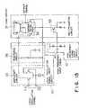
- FIG. 5 is a circuit diagram showing a detailed configuration of the frequency converter according to the first embodiment.
- the local oscillation signal input circuit 20 comprises a bias voltage source, an inductor 29, and a capacitor 27, which applies a bias potential to the multiplication circuit 30. Since the input circuit 20 has the even harmonic suppression means 21, an output impedance of the local oscillation signal input circuit 20 is small in a low frequency region in comparison with a local oscillation frequency, thereby suppressing a low-frequency noise occurring in the local oscillator (not shown) so as not to supply noises to the multiplication circuit 30. Because meaning of "frequency of multiple of even number of the local oscillation frequency" includes multiple of zero, and because it is possible to grasp the noise components having a frequency multiple of zero of the local oscillation frequency as a low-frequency noise.
- the even harmonic suppression means 21 comprises the inductor 29.
- the high-frequency signal input circuit 10 includes a capacitor and a voltage dividing resistor for dividing a supplied voltage.
- the multiplication circuit 30 comprises a load circuit 31, a transistor differential pair 32 as a switch for changing over plus and minus components in a bias-added local oscillation signal, and an amplifier circuit 33 for amplifying a bias-added high-frequency signal.
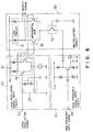
- FIG. 6 is a circuit diagram showing a configuration of a frequency converter according to a second embodiment.
- the local oscillation signal is amplified by a differential amplifier circuit 22 provided in the local oscillation signal input circuit 20. Since an output of the amplifier circuit 22 is connected to an inductor as the even harmonic noise suppression means 21, noise components having a low frequency are not amplified even though the local oscillation signal is amplified.
- an external noise component is suppressed, but also it is possible to suppress an internal noise component such as a thermal noise or shot noise, which is generated by each element provided in the local oscillation signal input circuit 20.
- an impedance matching circuit 23 is provided between the amplifier circuit 22 and an input terminal of the local oscillation signal so as to suppress a reflected wave of the local oscillation signal by establishing matching between a line impedance and an input impedance of the local oscillation signal.
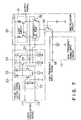
- FIG. 7 is a circuit diagram showing a configuration of the frequency converter according to a third embodiment.
- the local oscillation signal input circuit 20 comprises differential amplifier circuit 22 and an emitter-follower circuit 24, it is possible to suppress a low-frequency noise because differential outputs of the emitter-follower circuit 24 are connected through inductor 29 as the even harmonic suppression means 21.
- the local oscillation signal input circuit 20 comprises an impedance matching circuit 23, the differential amplifier circuit 22, the emitter-follower circuit 24, and the inductor as the even harmonic noise suppression means 21.
- the impedance matching circuit 23 has a main object to match an impedance between the output impedance of the local oscillation circuit or the line impedance of a transmission line with the input impedance of the differential amplifier circuit, also has a band pass characteristic for suppressing signals having other frequencies because the circuit 23 performs a matching at the local oscillation frequency. Accordingly, even though the matching circuit 23 is required to have an effect for suppressing the even harmonic wave noises, it is impossible for only the matching circuit 23 to expect an effect for suppressing the noises occurring in the differential amplifier circuit 22 and the emitter-follower circuit 24. It is possible to suppress the noises flowing into the multiplication circuit 30 by a connection of the inductor as the even harmonic suppression means 21 between both the outputs of the emitter-follower circuit 24 in addition to the matching circuit 23.
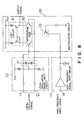
- FIG. 8 is a circuit diagram showing a frequency converter according to a fourth embodiment of the present invention. Since a bias voltage or current is supplied through the inductor as the even harmonic suppression means 21 to base terminals of both transistors constituting a differential pair 33 provided in the multiplication circuit 30, the low-frequency noise can be suppressed before supplying to the multiplication circuit 30. Even though values of two capacitors and inductor as the noise suppression means 21 can exhibit a function as the impedance matching circuit, the local oscillation signal input circuit 20 according to the present invention has a excellent function that the inductor can extremely suppress the low-frequency noises.
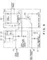
- FIG. 9 is a circuit diagram showing a frequency converter according to a fifth embodiment of the present invention.
- the frequency converter has a circuitry comprising a series resonance circuit 25 comprised of an inductor L2 and a capacitor C2 in order to further suppress noises having a frequency substantially two time greater than the local oscillation frequency in addition to the low-frequency. Since the inductor L2 and capacitor C2 constitute the series resonance circuit for resonating to the frequency substantially two times greater than the local oscillation frequency, an impedance becomes lower at a frequency near the frequency two times greater than the local oscillation frequency region. An inductor L1 makes an impedance lower in the low-frequency.
- the inductors L1 and L2 and capacitor C2 perform a parallel resonance in the local oscillation frequency, an impedance becomes higher, thereby causing an input voltage of the multiplication circuit 30 to have only the local oscillation frequency. Accordingly, since the circuit has a low impedance even in the low-frequency region, it is possible to suppress both the low-frequency noises and noises having a frequency near the frequency two times greater than the local oscillation frequency at the same time.
- FIG. 10 is a circuit diagram showing a configuration of a frequency converter according to a sixth embodiment of the present invention. Since the even harmonic suppression means 21 is provided before the output of the local oscillation signal input circuit 20 and comprises inductors L1 and L2 and a parallel resonance circuit L3 and C3, it is possible to suppress the low-frequency noises and the noises having a frequency near the frequency two times greater than the local oscillation frequency. At the same time, it is possible to obtain a high gain by resonating the inductors L1, L2 and L3 and the capacitor C3 at the local oscillation frequency.
- FIG. 11 is a block diagram showing a frequency converter according to a seventh embodiment of the present invention.
- the local oscillation signal is amplified by amplifier circuit 22 in local oscillation signal input circuit 20, and supplied to multiplication circuit 30 after the noises having a frequency near the frequency which is multiple of even number of the local oscillation frequency is suppressed by a reactance circuit 26.
- the reactance circuit 26 can be realized by connecting a short stub having a quarter wavelength, for example.
- FIG. 12 is a circuit diagram showing a frequency converter according to an eighth embodiment as a detailed constructual example of a reactance circuit, which is a ladder-type filter.
- inductors L1, L2 and L3 respectively resonate in series with capacitors C1, C2 and C3 at the local oscillation frequency
- inductors L4, L5 and L6 respectively resonate in series with capacitors C4, C5 and C6 at frequencies two, four and six times greater than the local oscillation frequency, respectively
- an inductor L7 resonates in parallel with a capacitor C7 at the local oscillation frequency.
- FIG. 13 shows a correlation between a transfer function represented on the ordinate and normalized frequencies represented on the abscissa.
- FIG. 14 is a circuit diagram showing a frequency converter according to a ninth embodiment as another constructual example of the reactance circuit.
- this embodiment it is possible to suppress the noises by a series resonance circuit which resonates in series with a frequency multiple of even number of the frequency of the local oscillation signal and which is connected in parallel with both outputs of the local oscillation input circuit 20.
- FIG. 15 is a circuit diagram showing a frequency converter according to a tenth embodiment as still further constructual example of the reactance circuit.
- a reactance circuit 26 comprises a pair of transmission lines of a quarter-wavelength short stub, and a voltage reference source which is connected with a junction point between the pair of lines. According to the configuration, it is possible to suppress noise components of frequencies multiple of zero, two, four and six of a fundamental frequency of the local oscillation signal as shown in FIG. 13, respectively.
- FIG. 16 is a circuit diagram showing a frequency converter according to an eleventh embodiment as a concrete example of a double balance multiplication circuit.
- the double balance multiplication circuit has as an output a differential component between F(t) and the high-frequency input, namely, the product of "Irf1(t)-Irf2" and does not have as an output a pulse width modulated signal caused from a product of F(t) and Iee such as the single balance multiplication circuit.
- the actual circuit has an error, Iee1 and Iee2 do not cancel completely each other, thereby resulting an appearance as a pulse width modulated signal the product of F(t) and an error component "Iee1-Iee2" included in an output.
- the double balance multiplication circuit can reduce influence of noises of a frequency which is multiple of even number of the local oscillation frequency, it is possible to further reduce the noises by removing the low-frequency noises by the local oscillation signal input circuit using inductors shown in FIG. 16. Furthermore, the noise suppression effect can improve more and more by means of a combination of the double balance type multiplication circuit and the local oscillation signal input circuit including the reactance circuit for suppressing the noise component having a frequency which is multiple of even-number of the local oscillation frequency.
- FIG. 17 shows a frequency converter according to a twelfth embodiment as a preferred example applied to a receiver system.
- the frequency converter according to a twelfth embodiment applies to a direct conversion receiver system, and there is shown in FIG. 17 an example in which an orthogonal demodulator is constituted from a frequency converter 41 according to the present invention. Since the frequency converter 41 receives a local oscillation frequency substantially the same as a frequency of a received signal to obtain a base band signal, this system is a kind of homodyne receiver systems.
- the base band signal of two channels is obtained by dividing the received signal into two kinds and converting frequencies of respective kind of the signal after both kinds of signal respectively have a phase difference of 90 degrees, for the purpose of distinguishing between the cases where the received signal frequency is higher than the frequency of the local oscillation signal and is lower than that.
- the local oscillation signal is supplied through a buffer amplifier 42 to two frequency converters 41A and 41B.
- Local oscillation signal input circuits 43 in the frequency converters 41 use spiral inductors realized by an integrated circuit to suppress the low-frequency noises as a noise near the frequency of multiple of zero of the local oscillation frequency, thereby realizing the orthogonal demodulator 40 having an excellent noise characteristic.
- An output of the frequency converter 41 is supplied to the differential single converter 45, which outputs a single end signal converted from the differential signal in order to supply a desired signal to base band frequency signal (a second intermediate frequency) signal processors 55A and 55B as shown in a system according to a thirteenth embodiment mentioned later.
- base band frequency signal a second intermediate frequency
- the buffer amplifier 42 has a matching function for matching a transmission line impedance of the local oscillation signal with an input impedance of the buffer amplifier.
- FIG. 18 is a block diagram showing a configuration of a receiver system according to a thirteenth embodiment using a direct conversion receiver system.
- a radio frequency signal which has been received by an antenna portion 51 is converted its frequency on the basis of a local oscillation signal having a frequency substantial the same as the radio frequency signal, so as to obtain a base band signal which will be outputted as received data after a demodulation.
- a high-frequency signal received by the antenna portion 51 is amplified by a high-frequency signal processor 52 and divided into two channels after an unnecessary frequency component is removed by a high-frequency filter.
- the frequency converter portion converts a frequency of the high-frequency signal by using a reference signal having a predetermined frequency substantially the same as that of the high-frequency signal.
- Base band signals formed by a frequency conversion are processed in base band signal processors 55A and 55B, respectively.
- a low-pass filter (not shown in the figure) eliminates the unnecessary high-frequency components and an A/D converter (not shown) converts a low component analog signal into a digital signal.
- an output portion 56 demodulates the digital signal by using an orthogonal rectifying detection system such as a delay rectify detector, and data signals such as voice, image and the like are reproduced.
- FIG. 19 is a block diagram showing a configuration of a receiver 60 according to a fourteenth embodiment and using a super heterodyne receiver system.
- a high-frequency signal processing section 61 selects a signal component in a desired frequency band from a received signal through an antenna 60A and amplifies a selected signal component to output a first intermediate frequency signal after a frequency conversion in a first signal converter 62.
- a first intermediate frequency signal processing section 63 removes an unnecessary frequency component and amplifies the unnecessary frequency component removed signal
- a second frequency converter 64 converts the first intermediate frequency signal into a second intermediate frequency signal.
- the second intermediate frequency signal is amplified in a second intermediate frequency signal processing section 65 after removing an unnecessary signal component, and an output section 66 outputs data signals including voices and images after a digital signal processing.
Landscapes
- Engineering & Computer Science (AREA)
- Power Engineering (AREA)
- Superheterodyne Receivers (AREA)
- Noise Elimination (AREA)
Applications Claiming Priority (3)
| Application Number | Priority Date | Filing Date | Title |
|---|---|---|---|
| JP47774/95 | 1995-02-13 | ||
| JP4777495 | 1995-02-13 | ||
| JP7047774A JPH08223065A (ja) | 1995-02-13 | 1995-02-13 | 周波数変換器 |
Publications (2)
| Publication Number | Publication Date |
|---|---|
| EP0726646A1 true EP0726646A1 (fr) | 1996-08-14 |
| EP0726646B1 EP0726646B1 (fr) | 2002-06-05 |
Family
ID=12784737
Family Applications (1)
| Application Number | Title | Priority Date | Filing Date |
|---|---|---|---|
| EP96102089A Expired - Lifetime EP0726646B1 (fr) | 1995-02-13 | 1996-02-13 | Converteur de fréquences capable de réduire les composantes de bruit dans des signaux d'oscillations locales |
Country Status (5)
| Country | Link |
|---|---|
| US (1) | US5634207A (fr) |
| EP (1) | EP0726646B1 (fr) |
| JP (1) | JPH08223065A (fr) |
| KR (1) | KR0178685B1 (fr) |
| DE (1) | DE69621481T2 (fr) |
Cited By (6)
| Publication number | Priority date | Publication date | Assignee | Title |
|---|---|---|---|---|
| GB2321149A (en) * | 1997-01-11 | 1998-07-15 | Plessey Semiconductors Ltd | Low voltage mixer |
| GB2321148A (en) * | 1997-01-11 | 1998-07-15 | Plessey Semiconductors Ltd | Mixer circuit with improved noise properties |
| EP0954093A1 (fr) * | 1998-04-29 | 1999-11-03 | Mitel, Inc. | Suppression des harmoniques d' ordre pair d' un oscillateur local |
| US6477360B1 (en) | 1999-03-09 | 2002-11-05 | Kabushiki Kaisha Toshiba | Frequency converter |
| WO2004023643A1 (fr) * | 2002-08-29 | 2004-03-18 | Infineon Technologies Ag | Circuit pourvu d'un convertisseur de frequence |
| EP1455442A3 (fr) * | 2003-03-06 | 2004-11-17 | Broadcom Corporation | Mélangeur à haute linéarité et tampon OL associé |
Families Citing this family (66)
| Publication number | Priority date | Publication date | Assignee | Title |
|---|---|---|---|---|
| KR100243489B1 (ko) * | 1995-11-22 | 2000-02-01 | 니시무로 타이죠 | 주파수 변환기 및 이를 이용한 무선 수신기 |
| US7515896B1 (en) | 1998-10-21 | 2009-04-07 | Parkervision, Inc. | Method and system for down-converting an electromagnetic signal, and transforms for same, and aperture relationships |
| US6061551A (en) | 1998-10-21 | 2000-05-09 | Parkervision, Inc. | Method and system for down-converting electromagnetic signals |
| US6560301B1 (en) | 1998-10-21 | 2003-05-06 | Parkervision, Inc. | Integrated frequency translation and selectivity with a variety of filter embodiments |
| US6370371B1 (en) | 1998-10-21 | 2002-04-09 | Parkervision, Inc. | Applications of universal frequency translation |
| US7236754B2 (en) | 1999-08-23 | 2007-06-26 | Parkervision, Inc. | Method and system for frequency up-conversion |
| US7039372B1 (en) | 1998-10-21 | 2006-05-02 | Parkervision, Inc. | Method and system for frequency up-conversion with modulation embodiments |
| US7295826B1 (en) | 1998-10-21 | 2007-11-13 | Parkervision, Inc. | Integrated frequency translation and selectivity with gain control functionality, and applications thereof |
| US6813485B2 (en) | 1998-10-21 | 2004-11-02 | Parkervision, Inc. | Method and system for down-converting and up-converting an electromagnetic signal, and transforms for same |
| US6542722B1 (en) | 1998-10-21 | 2003-04-01 | Parkervision, Inc. | Method and system for frequency up-conversion with variety of transmitter configurations |
| US7006805B1 (en) | 1999-01-22 | 2006-02-28 | Parker Vision, Inc. | Aliasing communication system with multi-mode and multi-band functionality and embodiments thereof, such as the family radio service |
| JP2000223951A (ja) * | 1999-01-27 | 2000-08-11 | Murata Mfg Co Ltd | 周波数逓倍器及びそれを用いた無線機器 |
| US6879817B1 (en) | 1999-04-16 | 2005-04-12 | Parkervision, Inc. | DC offset, re-radiation, and I/Q solutions using universal frequency translation technology |
| US6853690B1 (en) | 1999-04-16 | 2005-02-08 | Parkervision, Inc. | Method, system and apparatus for balanced frequency up-conversion of a baseband signal and 4-phase receiver and transceiver embodiments |
| US6873836B1 (en) | 1999-03-03 | 2005-03-29 | Parkervision, Inc. | Universal platform module and methods and apparatuses relating thereto enabled by universal frequency translation technology |
| US7110435B1 (en) | 1999-03-15 | 2006-09-19 | Parkervision, Inc. | Spread spectrum applications of universal frequency translation |
| US7693230B2 (en) | 1999-04-16 | 2010-04-06 | Parkervision, Inc. | Apparatus and method of differential IQ frequency up-conversion |
| US7110444B1 (en) | 1999-08-04 | 2006-09-19 | Parkervision, Inc. | Wireless local area network (WLAN) using universal frequency translation technology including multi-phase embodiments and circuit implementations |
| US7065162B1 (en) | 1999-04-16 | 2006-06-20 | Parkervision, Inc. | Method and system for down-converting an electromagnetic signal, and transforms for same |
| JP2001044858A (ja) | 1999-07-30 | 2001-02-16 | Nec Corp | 送信ミキサおよび2帯域出力切り替え高周波送信回路 |
| US8295406B1 (en) | 1999-08-04 | 2012-10-23 | Parkervision, Inc. | Universal platform module for a plurality of communication protocols |
| US7072390B1 (en) | 1999-08-04 | 2006-07-04 | Parkervision, Inc. | Wireless local area network (WLAN) using universal frequency translation technology including multi-phase embodiments |
| US7054296B1 (en) | 1999-08-04 | 2006-05-30 | Parkervision, Inc. | Wireless local area network (WLAN) technology and applications including techniques of universal frequency translation |
| US7082171B1 (en) | 1999-11-24 | 2006-07-25 | Parkervision, Inc. | Phase shifting applications of universal frequency translation |
| US7292835B2 (en) | 2000-01-28 | 2007-11-06 | Parkervision, Inc. | Wireless and wired cable modem applications of universal frequency translation technology |
| US7010286B2 (en) * | 2000-04-14 | 2006-03-07 | Parkervision, Inc. | Apparatus, system, and method for down-converting and up-converting electromagnetic signals |
| US7554508B2 (en) | 2000-06-09 | 2009-06-30 | Parker Vision, Inc. | Phased array antenna applications on universal frequency translation |
| US7454453B2 (en) | 2000-11-14 | 2008-11-18 | Parkervision, Inc. | Methods, systems, and computer program products for parallel correlation and applications thereof |
| US7010559B2 (en) | 2000-11-14 | 2006-03-07 | Parkervision, Inc. | Method and apparatus for a parallel correlator and applications thereof |
| US20020180383A1 (en) * | 2001-04-16 | 2002-12-05 | Mingfu Gong | Electronic HID ballast and a PPM method of preventing acoustic arc resonance |
| JP4920162B2 (ja) * | 2001-09-04 | 2012-04-18 | 株式会社東芝 | 周波数変換器及びこの周波数変換器を使用した通信装置 |
| US7085335B2 (en) * | 2001-11-09 | 2006-08-01 | Parkervision, Inc. | Method and apparatus for reducing DC offsets in a communication system |
| US7072427B2 (en) | 2001-11-09 | 2006-07-04 | Parkervision, Inc. | Method and apparatus for reducing DC offsets in a communication system |
| EP1319423A3 (fr) | 2001-12-11 | 2003-10-08 | Dornier Medtech System GmbH | Outil et procédé pour l'initiation des réactions chimiques et pour l'administration précise des médicaments et autres agents |
| US6975848B2 (en) | 2002-06-04 | 2005-12-13 | Parkervision, Inc. | Method and apparatus for DC offset removal in a radio frequency communication channel |
| US7321640B2 (en) * | 2002-06-07 | 2008-01-22 | Parkervision, Inc. | Active polyphase inverter filter for quadrature signal generation |
| US7379883B2 (en) | 2002-07-18 | 2008-05-27 | Parkervision, Inc. | Networking methods and systems |
| US7460584B2 (en) | 2002-07-18 | 2008-12-02 | Parkervision, Inc. | Networking methods and systems |
| US20040116095A1 (en) * | 2002-12-10 | 2004-06-17 | Irf Semiconductor, Inc. | High dynamic range radio frequency mixer |
| DE602005006585D1 (de) * | 2004-07-06 | 2008-06-19 | Acp Advanced Circuit Pursuit A | Symmetrischer mischer mit fets |
| US7620382B2 (en) * | 2005-06-09 | 2009-11-17 | Alps Electric Co., Ltd. | Frequency converter capable of preventing level of intermediate frequency signal from lowering due to rise in temperature |
| JP4885643B2 (ja) * | 2006-08-09 | 2012-02-29 | 新日本無線株式会社 | ミキサ回路 |
| US7812827B2 (en) | 2007-01-03 | 2010-10-12 | Apple Inc. | Simultaneous sensing arrangement |
| US8493331B2 (en) | 2007-06-13 | 2013-07-23 | Apple Inc. | Touch detection using multiple simultaneous frequencies |
| US8275314B1 (en) | 2007-08-13 | 2012-09-25 | Marvell International Ltd. | Bluetooth scan modes |
| US8577305B1 (en) | 2007-09-21 | 2013-11-05 | Marvell International Ltd. | Circuits and methods for generating oscillating signals |
| JP2008092590A (ja) * | 2007-10-25 | 2008-04-17 | Seiko Epson Corp | 電子装置及び通信方法 |
| US20090131000A1 (en) * | 2007-11-21 | 2009-05-21 | Kuo Yao H | Radio receiver system |
| US8588705B1 (en) | 2007-12-11 | 2013-11-19 | Marvell International Ltd. | System and method of determining Power over Ethernet impairment |
| US8072255B2 (en) * | 2008-01-07 | 2011-12-06 | Qualcomm Incorporated | Quadrature radio frequency mixer with low noise and low conversion loss |
| EP2289274B1 (fr) | 2008-06-16 | 2016-11-23 | Marvell World Trade Ltd. | Communication sans fil à courte portée |
| US8600324B1 (en) | 2008-06-27 | 2013-12-03 | Marvell International Ltd | Circuit and method for adjusting a digitally controlled oscillator |
| US8472968B1 (en) | 2008-08-11 | 2013-06-25 | Marvell International Ltd. | Location-based detection of interference in cellular communications systems |
| US9288764B1 (en) | 2008-12-31 | 2016-03-15 | Marvell International Ltd. | Discovery-phase power conservation |
| US8472427B1 (en) | 2009-04-06 | 2013-06-25 | Marvell International Ltd. | Packet exchange arbitration for coexisting radios |
| US9036650B2 (en) * | 2009-09-11 | 2015-05-19 | Apple Inc. | Automatic low noise frequency selection |
| US9066369B1 (en) | 2009-09-16 | 2015-06-23 | Marvell International Ltd. | Coexisting radio communication |
| US8767771B1 (en) | 2010-05-11 | 2014-07-01 | Marvell International Ltd. | Wakeup beacons for mesh networks |
| EP2630827B1 (fr) | 2010-10-20 | 2018-11-21 | Marvell World Trade Ltd. | Découverte de service avant l'association |
| US8750278B1 (en) | 2011-05-26 | 2014-06-10 | Marvell International Ltd. | Method and apparatus for off-channel device invitation |
| US8983557B1 (en) | 2011-06-30 | 2015-03-17 | Marvell International Ltd. | Reducing power consumption of a multi-antenna transceiver |
| US9125216B1 (en) | 2011-09-28 | 2015-09-01 | Marvell International Ltd. | Method and apparatus for avoiding interference among multiple radios |
| US8670741B2 (en) * | 2011-12-21 | 2014-03-11 | Triquint Semiconductor, Inc. | Mixer with high second-order and third-order intercept point |
| WO2013119810A1 (fr) | 2012-02-07 | 2013-08-15 | Marvell World Trade Ltd. | Procédé et appareil pour la communication multi-réseaux |
| US9450649B2 (en) | 2012-07-02 | 2016-09-20 | Marvell World Trade Ltd. | Shaping near-field transmission signals |
| US10057093B2 (en) | 2016-06-29 | 2018-08-21 | International Business Machines Corporation | Using common mode local oscillator termination in single-ended commutating circuits for conversion gain improvement |
Citations (4)
| Publication number | Priority date | Publication date | Assignee | Title |
|---|---|---|---|---|
| US4184120A (en) * | 1975-08-28 | 1980-01-15 | Toshihiko Teshirogi | Mixing circuit |
| EP0051179A1 (fr) * | 1980-11-03 | 1982-05-12 | Siemens Aktiengesellschaft | Circuit oscillateur pouvant être intégré |
| US4361910A (en) * | 1981-06-15 | 1982-11-30 | Teller Jr Howard S | Ground loop injection VHF tuner |
| US4369522A (en) * | 1978-07-03 | 1983-01-18 | Motorola, Inc. | Singly-balanced active mixer circuit |
Family Cites Families (5)
| Publication number | Priority date | Publication date | Assignee | Title |
|---|---|---|---|---|
| US3659206A (en) * | 1970-07-16 | 1972-04-25 | Collins Radio Co | Microwave balanced mixer circuit |
| US5113094A (en) * | 1990-03-13 | 1992-05-12 | Wiltron Company | Method and apparatus for increasing the high frequency sensitivity response of a sampler frequency converter |
| JP3419484B2 (ja) * | 1992-03-30 | 2003-06-23 | 株式会社東芝 | 変調器、送信器 |
| US5446923A (en) * | 1994-03-03 | 1995-08-29 | B.E.L.-Tronics Limited | Mixer using fundamental frequency or second or third harmonic frequencies of a local oscillator for maximized resultant frequency mixer product |
| US5469120A (en) * | 1994-12-07 | 1995-11-21 | Lsi Logic Corporation | High performance voltage controlled oscillator |
-
1995
- 1995-02-13 JP JP7047774A patent/JPH08223065A/ja active Pending
-
1996
- 1996-02-12 US US08/600,115 patent/US5634207A/en not_active Expired - Lifetime
- 1996-02-13 DE DE69621481T patent/DE69621481T2/de not_active Expired - Lifetime
- 1996-02-13 KR KR1019960003405A patent/KR0178685B1/ko not_active Expired - Fee Related
- 1996-02-13 EP EP96102089A patent/EP0726646B1/fr not_active Expired - Lifetime
Patent Citations (4)
| Publication number | Priority date | Publication date | Assignee | Title |
|---|---|---|---|---|
| US4184120A (en) * | 1975-08-28 | 1980-01-15 | Toshihiko Teshirogi | Mixing circuit |
| US4369522A (en) * | 1978-07-03 | 1983-01-18 | Motorola, Inc. | Singly-balanced active mixer circuit |
| EP0051179A1 (fr) * | 1980-11-03 | 1982-05-12 | Siemens Aktiengesellschaft | Circuit oscillateur pouvant être intégré |
| US4361910A (en) * | 1981-06-15 | 1982-11-30 | Teller Jr Howard S | Ground loop injection VHF tuner |
Cited By (15)
| Publication number | Priority date | Publication date | Assignee | Title |
|---|---|---|---|---|
| US6211718B1 (en) | 1997-01-11 | 2001-04-03 | Motel Semiconductor Limited | Low voltage double balanced mixer |
| GB2321149A (en) * | 1997-01-11 | 1998-07-15 | Plessey Semiconductors Ltd | Low voltage mixer |
| GB2321148A (en) * | 1997-01-11 | 1998-07-15 | Plessey Semiconductors Ltd | Mixer circuit with improved noise properties |
| EP0853373A1 (fr) * | 1997-01-11 | 1998-07-15 | Plessey Semiconductors Limited | Mélangeur équilibré double |
| GB2321149B (en) * | 1997-01-11 | 2001-04-04 | Plessey Semiconductors Ltd | Low voltage double balanced mixer |
| GB2321148B (en) * | 1997-01-11 | 2000-10-25 | Plessey Semiconductors Ltd | Double balanced mixer |
| EP0853376A1 (fr) * | 1997-01-11 | 1998-07-15 | Plessey Semiconductors Limited | Mélangeur doublement équiliblé à basse tension |
| EP0954093A1 (fr) * | 1998-04-29 | 1999-11-03 | Mitel, Inc. | Suppression des harmoniques d' ordre pair d' un oscillateur local |
| KR100371876B1 (ko) * | 1999-03-09 | 2003-02-11 | 가부시끼가이샤 도시바 | 주파수 변환회로 |
| US6477360B1 (en) | 1999-03-09 | 2002-11-05 | Kabushiki Kaisha Toshiba | Frequency converter |
| WO2004023643A1 (fr) * | 2002-08-29 | 2004-03-18 | Infineon Technologies Ag | Circuit pourvu d'un convertisseur de frequence |
| EP1455442A3 (fr) * | 2003-03-06 | 2004-11-17 | Broadcom Corporation | Mélangeur à haute linéarité et tampon OL associé |
| US6972610B2 (en) | 2003-03-06 | 2005-12-06 | Broadcom Corporation | High linearity passive mixer and associated LO buffer |
| US6989705B2 (en) | 2003-03-06 | 2006-01-24 | Broadcom Corporation | High linearity passive mixer and associated LO buffer |
| US7102411B2 (en) | 2003-03-06 | 2006-09-05 | Broadcom Corporation | High linearity passive mixer and associated LO buffer |
Also Published As
| Publication number | Publication date |
|---|---|
| DE69621481D1 (de) | 2002-07-11 |
| KR0178685B1 (ko) | 1999-04-01 |
| EP0726646B1 (fr) | 2002-06-05 |
| US5634207A (en) | 1997-05-27 |
| JPH08223065A (ja) | 1996-08-30 |
| DE69621481T2 (de) | 2002-12-12 |
| KR960032887A (ko) | 1996-09-17 |
Similar Documents
| Publication | Publication Date | Title |
|---|---|---|
| EP0726646B1 (fr) | Converteur de fréquences capable de réduire les composantes de bruit dans des signaux d'oscillations locales | |
| KR100314798B1 (ko) | 집적화된이미지제거믹서 | |
| US6035186A (en) | Integrated receiver | |
| US6510314B1 (en) | Mixer circuit with output stage for implementation on integrated circuit | |
| EP0643494A1 (fr) | Récepteur | |
| US7231192B2 (en) | High frequency receiver | |
| US20030112895A1 (en) | Intergrated frequency translation and selectivity | |
| US20030007377A1 (en) | Frequency converter and radio communication apparatus with the same | |
| US6449471B1 (en) | Wireless terminal device | |
| US7477886B1 (en) | Cascading-synchronous mixer and method of operation | |
| JPH11341098A (ja) | 無線装置 | |
| US6507627B1 (en) | Direct conversion receiving apparatus with DC component cut function | |
| JP3164008B2 (ja) | 無線受信機 | |
| US7085548B1 (en) | Harmonic mixer | |
| US5736840A (en) | Phase shifter and communication system using the phase shifter | |
| US20060088122A1 (en) | Direct-conversion frequency mixer | |
| US6671505B1 (en) | Frequency converter | |
| JP3452782B2 (ja) | 偶高調波ミクサ、直交ミクサ、イメージリジェクションミクサ、送信装置および受信装置 | |
| EP0570125A1 (fr) | Circuit de conversion dissymétrique-symétrique utilisé comme circuit d'entrée d'un mélangeur | |
| US6970687B1 (en) | Mixer | |
| EP0469169A1 (fr) | Mélangeur convertisseur de fréquence | |
| US5650714A (en) | Orthogonal signal generation system | |
| US6335659B1 (en) | Demodulator circuits | |
| RU2067787C1 (ru) | Двухкаскадный преобразователь частоты с подавлением зеркального канала | |
| US6990326B2 (en) | Image suppression filter circuit |
Legal Events
| Date | Code | Title | Description |
|---|---|---|---|
| PUAI | Public reference made under article 153(3) epc to a published international application that has entered the european phase |
Free format text: ORIGINAL CODE: 0009012 |
|
| 17P | Request for examination filed |
Effective date: 19960213 |
|
| AK | Designated contracting states |
Kind code of ref document: A1 Designated state(s): DE FR GB |
|
| 17Q | First examination report despatched |
Effective date: 19991029 |
|
| GRAG | Despatch of communication of intention to grant |
Free format text: ORIGINAL CODE: EPIDOS AGRA |
|
| GRAG | Despatch of communication of intention to grant |
Free format text: ORIGINAL CODE: EPIDOS AGRA |
|
| GRAH | Despatch of communication of intention to grant a patent |
Free format text: ORIGINAL CODE: EPIDOS IGRA |
|
| GRAH | Despatch of communication of intention to grant a patent |
Free format text: ORIGINAL CODE: EPIDOS IGRA |
|
| GRAA | (expected) grant |
Free format text: ORIGINAL CODE: 0009210 |
|
| AK | Designated contracting states |
Kind code of ref document: B1 Designated state(s): DE FR GB |
|
| REG | Reference to a national code |
Ref country code: GB Ref legal event code: FG4D |
|
| REF | Corresponds to: |
Ref document number: 69621481 Country of ref document: DE Date of ref document: 20020711 |
|
| ET | Fr: translation filed | ||
| PLBE | No opposition filed within time limit |
Free format text: ORIGINAL CODE: 0009261 |
|
| 26N | No opposition filed |
Effective date: 20030306 |
|
| PGFP | Annual fee paid to national office [announced via postgrant information from national office to epo] |
Ref country code: FR Payment date: 20130301 Year of fee payment: 18 Ref country code: GB Payment date: 20130213 Year of fee payment: 18 Ref country code: DE Payment date: 20130206 Year of fee payment: 18 |
|
| REG | Reference to a national code |
Ref country code: DE Ref legal event code: R119 Ref document number: 69621481 Country of ref document: DE |
|
| GBPC | Gb: european patent ceased through non-payment of renewal fee |
Effective date: 20140213 |
|
| REG | Reference to a national code |
Ref country code: FR Ref legal event code: ST Effective date: 20141031 |
|
| REG | Reference to a national code |
Ref country code: DE Ref legal event code: R119 Ref document number: 69621481 Country of ref document: DE Effective date: 20140902 |
|
| PG25 | Lapsed in a contracting state [announced via postgrant information from national office to epo] |
Ref country code: FR Free format text: LAPSE BECAUSE OF NON-PAYMENT OF DUE FEES Effective date: 20140228 Ref country code: GB Free format text: LAPSE BECAUSE OF NON-PAYMENT OF DUE FEES Effective date: 20140213 Ref country code: DE Free format text: LAPSE BECAUSE OF NON-PAYMENT OF DUE FEES Effective date: 20140902 |