EP0730048A1 - Verfahren zur Züchtung einkristalliner Silizium aus der Dampfphase - Google Patents
Verfahren zur Züchtung einkristalliner Silizium aus der Dampfphase Download PDFInfo
- Publication number
- EP0730048A1 EP0730048A1 EP96301353A EP96301353A EP0730048A1 EP 0730048 A1 EP0730048 A1 EP 0730048A1 EP 96301353 A EP96301353 A EP 96301353A EP 96301353 A EP96301353 A EP 96301353A EP 0730048 A1 EP0730048 A1 EP 0730048A1
- Authority
- EP
- European Patent Office
- Prior art keywords
- single crystal
- silicon single
- ambience
- etching
- oxide film
- Prior art date
- Legal status (The legal status is an assumption and is not a legal conclusion. Google has not performed a legal analysis and makes no representation as to the accuracy of the status listed.)
- Granted
Links
- 238000000034 method Methods 0.000 title claims abstract description 28
- 238000001947 vapour-phase growth Methods 0.000 title claims abstract description 23
- 229910021421 monocrystalline silicon Inorganic materials 0.000 title 1
- 239000000758 substrate Substances 0.000 claims abstract description 52
- 239000013078 crystal Substances 0.000 claims abstract description 48
- 229910052710 silicon Inorganic materials 0.000 claims abstract description 48
- 239000010703 silicon Substances 0.000 claims abstract description 48
- XUIMIQQOPSSXEZ-UHFFFAOYSA-N Silicon Chemical compound [Si] XUIMIQQOPSSXEZ-UHFFFAOYSA-N 0.000 claims abstract description 47
- UFHFLCQGNIYNRP-UHFFFAOYSA-N Hydrogen Chemical compound [H][H] UFHFLCQGNIYNRP-UHFFFAOYSA-N 0.000 claims abstract description 37
- 238000005530 etching Methods 0.000 claims abstract description 35
- 239000011261 inert gas Substances 0.000 claims abstract description 13
- 238000010438 heat treatment Methods 0.000 claims abstract description 8
- 239000007789 gas Substances 0.000 claims description 29
- 239000010408 film Substances 0.000 claims description 28
- XKRFYHLGVUSROY-UHFFFAOYSA-N Argon Chemical compound [Ar] XKRFYHLGVUSROY-UHFFFAOYSA-N 0.000 claims description 26
- 239000010409 thin film Substances 0.000 claims description 14
- 229910052786 argon Inorganic materials 0.000 claims description 13
- 239000001307 helium Substances 0.000 claims description 3
- 229910052734 helium Inorganic materials 0.000 claims description 3
- SWQJXJOGLNCZEY-UHFFFAOYSA-N helium atom Chemical compound [He] SWQJXJOGLNCZEY-UHFFFAOYSA-N 0.000 claims description 3
- 229910052743 krypton Inorganic materials 0.000 claims description 3
- DNNSSWSSYDEUBZ-UHFFFAOYSA-N krypton atom Chemical compound [Kr] DNNSSWSSYDEUBZ-UHFFFAOYSA-N 0.000 claims description 3
- 229910052754 neon Inorganic materials 0.000 claims description 3
- GKAOGPIIYCISHV-UHFFFAOYSA-N neon atom Chemical compound [Ne] GKAOGPIIYCISHV-UHFFFAOYSA-N 0.000 claims description 3
- 229910052724 xenon Inorganic materials 0.000 claims description 3
- FHNFHKCVQCLJFQ-UHFFFAOYSA-N xenon atom Chemical compound [Xe] FHNFHKCVQCLJFQ-UHFFFAOYSA-N 0.000 claims description 3
- 239000001257 hydrogen Substances 0.000 description 9
- 229910052739 hydrogen Inorganic materials 0.000 description 9
- VEXZGXHMUGYJMC-UHFFFAOYSA-N Hydrochloric acid Chemical compound Cl VEXZGXHMUGYJMC-UHFFFAOYSA-N 0.000 description 6
- 229910000041 hydrogen chloride Inorganic materials 0.000 description 6
- IXCSERBJSXMMFS-UHFFFAOYSA-N hydrogen chloride Substances Cl.Cl IXCSERBJSXMMFS-UHFFFAOYSA-N 0.000 description 6
- IJGRMHOSHXDMSA-UHFFFAOYSA-N Atomic nitrogen Chemical compound N#N IJGRMHOSHXDMSA-UHFFFAOYSA-N 0.000 description 5
- 238000010586 diagram Methods 0.000 description 4
- 238000002474 experimental method Methods 0.000 description 4
- VYPSYNLAJGMNEJ-UHFFFAOYSA-N Silicium dioxide Chemical compound O=[Si]=O VYPSYNLAJGMNEJ-UHFFFAOYSA-N 0.000 description 3
- 238000004519 manufacturing process Methods 0.000 description 3
- 230000015572 biosynthetic process Effects 0.000 description 2
- 238000011109 contamination Methods 0.000 description 2
- 238000007796 conventional method Methods 0.000 description 2
- 238000005260 corrosion Methods 0.000 description 2
- 230000007797 corrosion Effects 0.000 description 2
- 229910052757 nitrogen Inorganic materials 0.000 description 2
- 229910052681 coesite Inorganic materials 0.000 description 1
- 229910052906 cristobalite Inorganic materials 0.000 description 1
- 230000001627 detrimental effect Effects 0.000 description 1
- 229910001873 dinitrogen Inorganic materials 0.000 description 1
- 150000004767 nitrides Chemical class 0.000 description 1
- 235000015097 nutrients Nutrition 0.000 description 1
- 230000005855 radiation Effects 0.000 description 1
- 230000000717 retained effect Effects 0.000 description 1
- 150000003376 silicon Chemical class 0.000 description 1
- 239000000377 silicon dioxide Substances 0.000 description 1
- 229910052682 stishovite Inorganic materials 0.000 description 1
- ZDHXKXAHOVTTAH-UHFFFAOYSA-N trichlorosilane Chemical compound Cl[SiH](Cl)Cl ZDHXKXAHOVTTAH-UHFFFAOYSA-N 0.000 description 1
- 239000005052 trichlorosilane Substances 0.000 description 1
- 229910052905 tridymite Inorganic materials 0.000 description 1
Images


Classifications
-
- C—CHEMISTRY; METALLURGY
- C30—CRYSTAL GROWTH
- C30B—SINGLE-CRYSTAL GROWTH; UNIDIRECTIONAL SOLIDIFICATION OF EUTECTIC MATERIAL OR UNIDIRECTIONAL DEMIXING OF EUTECTOID MATERIAL; REFINING BY ZONE-MELTING OF MATERIAL; PRODUCTION OF A HOMOGENEOUS POLYCRYSTALLINE MATERIAL WITH DEFINED STRUCTURE; SINGLE CRYSTALS OR HOMOGENEOUS POLYCRYSTALLINE MATERIAL WITH DEFINED STRUCTURE; AFTER-TREATMENT OF SINGLE CRYSTALS OR A HOMOGENEOUS POLYCRYSTALLINE MATERIAL WITH DEFINED STRUCTURE; APPARATUS THEREFOR
- C30B29/00—Single crystals or homogeneous polycrystalline material with defined structure characterised by the material or by their shape
- C30B29/02—Elements
- C30B29/06—Silicon
-
- C—CHEMISTRY; METALLURGY
- C30—CRYSTAL GROWTH
- C30B—SINGLE-CRYSTAL GROWTH; UNIDIRECTIONAL SOLIDIFICATION OF EUTECTIC MATERIAL OR UNIDIRECTIONAL DEMIXING OF EUTECTOID MATERIAL; REFINING BY ZONE-MELTING OF MATERIAL; PRODUCTION OF A HOMOGENEOUS POLYCRYSTALLINE MATERIAL WITH DEFINED STRUCTURE; SINGLE CRYSTALS OR HOMOGENEOUS POLYCRYSTALLINE MATERIAL WITH DEFINED STRUCTURE; AFTER-TREATMENT OF SINGLE CRYSTALS OR A HOMOGENEOUS POLYCRYSTALLINE MATERIAL WITH DEFINED STRUCTURE; APPARATUS THEREFOR
- C30B25/00—Single-crystal growth by chemical reaction of reactive gases, e.g. chemical vapour-deposition growth
- C30B25/02—Epitaxial-layer growth
Definitions
- This invention relates to a method for the vapor-phase growth of a thin film of silicon single crystal on a silicon single crystal substrate. More particularly, this invention relates to an ambience which is prepared for the vapor-phase growth of a thin film of silicon single crystal.
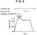
- the temperature of the substrate has been raised in an ambience of hydrogen gas.
- this silicon single crystal substrate is transported from a preceding chamber whose ambience of air is displaced with an ambience of nitrogen gas in advance into a reaction vessel having a temperature near 900°C, for example, this silicon single crystal substrate is heated in the ambience of hydrogen gas up to an etching temperature of desirable degree as shown in Fig. 6.
- the conventional method of this principle has the possibility of giving rise to a minute undulation (small hills and valleys) called microroughness in a wide area of the epiwafer surface.
- microroughness a minute undulation (small hills and valleys)
- the epiwafer surface is illuminated under a focused beam of light in a dark room, the area with large microroughness scatters the incident light randomly and appears to be a white cloud, which is popularly referred to as "cloud” or "haze.”
- the epiwafer surface has the surface free from microroughness.
- This invention produced in the light of the true state of prior art mentioned above, has for an object thereof the provision of a method for the vapor-phase growth which allows an epiwafer having a smooth surface free from microroughness to be produced infallibly and also the provision of a method for the vapor-phase growth which affects the etching of the silicon single crystal substrate by a process instead of the conventional process using hydrogen chloride gas.
- the step of heat-up in the ambience of an inert gas is continued until the temperature reaches a level appropriate for the removal of the native oxide film formed on the surface of said silicon single crystal substrate by the etching with hydrogen gas.
- the above step is desirably started at a temperature of less than 800 °C.
- the temperature which is appropriate for the removal of the native oxide film by the etching with hydrogen gas is such that the rate of etching the native oxide film caused by the hydrogen gas is not less than 1/10 of the rate of etching silicon single crystal. Specifically, this temperature is not less than 950°C and not more than 1190°C, for example.
- the inert gas to be used appropriately is one gas species selected from the group consisting of helium, neon, argon, krypton, and xenon or a rare gas prepared by mixing two or more gases selected from the group.
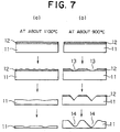
- the present inventor has searched for the cause of the generation of microroughness and has consequently found that when a native oxide film (SiO 2 ) with a thickness of about 1.5 nm on the surface of a silicon single crystal substrate is etched during heating up the silicon single crystal substrate in an ambience of hydrogen gas, the etching gives a small pits as indicated in Fig. 7 (b) and the surface of the silicon single crystal substrate 11 begins to be etched sequentially from a part 13 where a native oxide film 12 has been completely removed and, as a result, forms therein a part etched deeply with the hydrogen gas and a part etched shallowly therewith, and ultimately induces the formation of an undulation 14 (small hills and valleys) on the surface of the silicon single crystal substrate 11.
- a native oxide film SiO 2
- the native oxide film 12 When heated in an ambience of hydrogen to a temperature of not less than about 800°C, the native oxide film 12 is etched by hydrogen without use of hydrogen chloride gas. At temperatures in the approximate range of 800°C to 900°C, the native oxide film 12 is removed incompletely on the entire surface of the silicon single crystal substrate 11. In the environment of this etching, the surface of the substrate 11 is divided into two parts; in the one part the etching of the native oxide film proceeds quickly and the surface of silicon single crystal substrate 11 is exposed quickly to the ambience of hydrogen and such quick etching as mentioned above does not proceed in the other part.
- the etching rate of hydrogen at about 900°C is about 0.7 nm/min for the silicon single crystal substrate and about 0.05 nm/min for the native oxide film.
- the etching rate of the silicon single crystal substrate exhibited by hydrogen is about 14 times higher than that on the native oxide film.
- the part exposed is etched at a rate about 14 times higher than the etching rate of the native oxide film 12.
- This undulation 14 causes microroughness.
- the silicon single crystal substrate is transported into the reaction vessel enclosing therewith an ambience of hydrogen at a temperature near 900°C which is the temperature to amplify the unevenness of the surface due to the hydrogen etching of the native oxide film as has been observed conventionally, the microroughening inevitably occurs because the period kept at about 900°C before starting the heating-up process is elongated as a natural consequence.
- the etching rate of the native oxide film by hydrogen is about 1 nm/min; this value is roughly 20 times higher than that at a temperature near 900°C, and the rate of etching is roughly equal to that of the silicon single crystal substrate.
- the temperature of the silicon single crystal substrate is raised in an ambience of an inert gas so as to preclude the otherwise possible removal of the native oxide film.
- the hydrogen gas is introduced to contact with the silicon single crystal substrate.
- the native oxide film on the surface of silicon single crystal substrate is quickly removed over the entire area thereof.
- the etching rate of hydrogen gas is substantially equal between the native oxide film and of the silicon single crystal substrate, the unevenness of etching the native oxide film is not amplified on the surface of the substrate as shown in Fig. 7 (a) and the microroughness can not be increased.
- Fig. 1 shows a process for the production of a thin film of silicon single crystal following the method of this invention for the vapor-phase growth.
- a cold wall type apparatus for vapor-phase growth as shown in Fig. 2 is used to perform vapor-phase growth of a thin film 2 of silicon single crystal (hereinafter referred to as "thin film 2") on the surface of a silicon single crystal substrate 1 (hereinafter referred to as "substrate 1").
- the apparatus for vapor-phase growth mentioned above is a horizontal single-wafer apparatus for vapor-phase growth which is provided, as shown in Fig. 2, with a reaction vessel 3 made of transparent quartz glass, an infrared radiation heating lamp 4 set in place outside the reaction vessel 3, a gas inlet 5 for a gas 8 to be used for the vapor-phase growth, a gas outlet 6, and a gate valve 7.
- the substrate 1 is first transported from a preceding chamber (not shown) enclosing therewith an ambience of nitrogen through the gate valve 7 into the reaction vessel 3 kept cooled at about 700°C and it is then set horizontally inside the reaction vessel 3.
- the interior of the reaction vessel is displaced in advance with argon gas. The process for heating up the substrate 1 begins as soon as the substrate 1 is set in the reaction vessel 3.
- the heating-up process in the ambience of argon gas was started immediately after completion of the transporting the substrate 1 into the reaction vessel 3 and was continued to reach the relevant temperature condition. Subsequently, the interior of the reaction vessel 3 was displaced with an ambience of hydrogen gas. In the present experiment, the conditions for increasing microroughness were obtained by retaining the substrate 1 under the relevant temperature condition for 3 minutes.
- the substrate 1 was retained in the ambience of hydrogen gas at 1100°C for two minutes to attain complete removal of the native oxide film. Thereafter, with trichlorosilane as a source gas, the thin film 2 was grown in a thickness of about 6 ⁇ m at a temperature of 1100°C over a period of 2 minutes.
- the surface of the thin film 2 grown in consequence of the present experiment was observed using the atomic force microscope.
- the results are the graphs of Fig. 3 through Fig. 5. It is noted from the graph of Fig. 3 that the substrate was deeply etched and the microroughness was notably serious when the interior of the reaction vessel 3 was displaced with the ambience of hydrogen gas at 900°C. In contrast, at the temperatures of 1000°C and 1100°C, virtually no sign of etching was observed on the surface of the substrate as indicated by the data of Fig. 4 and Fig. 5.
- the micro-roughness occurred when the interior of the reaction vessel 3 was displaced with an ambience of hydrogen gas at a temperature in the approximate range of 800°C to 900°C. It was further found that the occurrence of microroughness could be prevented so long as the temperature to switch the ambience from an inert gas to hydrogen was not less than 950°C, at which the etching rate of the native oxide film by hydrogen gas exceeded 1/10 of the etching rate on the silicon single crystal. If the temperature of the substrate of silicon single crystal exceeds 1190°C, however, the disadvantage will appear that detriments such as the phenomena of autodoping and slippage cannot be ignored.
- the present embodiment contemplates using argon gas as an inert gas.
- the inert gas need not be limited to argon gas but may be one selected from the group consisting of helium, neon, krypton, and xenon or a rare gas prepared by mixing two or more gases selected from the group. It is also allowable to use nitrogen as the inert gas, however, the nitride formation must be cared.
- the method of this invention for the vapor-phase growth allows an epiwafer of a smooth surface free from microroughness to be produced because the silicon single crystal substrate is heated up to the temperature higher than 800 or 900 °C in an ambience of an inert gas for preventing the native oxide film from being unevenly etched.
- the method can preclude the problem that the use of hydrogen chloride gas results in metallic contamination at the substrate surface and autodoping.
Landscapes
- Chemical & Material Sciences (AREA)
- Engineering & Computer Science (AREA)
- Crystallography & Structural Chemistry (AREA)
- Materials Engineering (AREA)
- Metallurgy (AREA)
- Organic Chemistry (AREA)
- Chemical Kinetics & Catalysis (AREA)
- General Chemical & Material Sciences (AREA)
- Drying Of Semiconductors (AREA)
- Crystals, And After-Treatments Of Crystals (AREA)
- Chemical Vapour Deposition (AREA)
Applications Claiming Priority (3)
| Application Number | Priority Date | Filing Date | Title |
|---|---|---|---|
| JP6688395 | 1995-03-01 | ||
| JP66883/95 | 1995-03-01 | ||
| JP7066883A JPH08236462A (ja) | 1995-03-01 | 1995-03-01 | 気相成長方法 |
Publications (2)
| Publication Number | Publication Date |
|---|---|
| EP0730048A1 true EP0730048A1 (de) | 1996-09-04 |
| EP0730048B1 EP0730048B1 (de) | 1999-11-03 |
Family
ID=13328743
Family Applications (1)
| Application Number | Title | Priority Date | Filing Date |
|---|---|---|---|
| EP96301353A Expired - Lifetime EP0730048B1 (de) | 1995-03-01 | 1996-02-28 | Verfahren zur Züchtung einkristalliner Silizium aus der Dampfphase |
Country Status (4)
| Country | Link |
|---|---|
| US (1) | US5718762A (de) |
| EP (1) | EP0730048B1 (de) |
| JP (1) | JPH08236462A (de) |
| DE (1) | DE69604948T2 (de) |
Cited By (5)
| Publication number | Priority date | Publication date | Assignee | Title |
|---|---|---|---|---|
| WO1999035311A1 (en) * | 1998-01-09 | 1999-07-15 | Asm America, Inc. | In situ growth of oxide and silicon layers |
| EP1069601A4 (de) * | 1998-03-27 | 2001-10-24 | Super Silicon Crystal Res Inst | Verfahren zum herstellen halbleiterscheiben |
| WO2001086034A3 (en) * | 2000-05-08 | 2002-02-21 | Memc Electronic Materials | Modified susceptor for use in chemical vapor deposition process |
| WO2003088332A1 (fr) * | 2002-04-17 | 2003-10-23 | Tokyo Electron Limited | Procede de formation d'une couche epitaxiale de silicium |
| US6749687B1 (en) | 1998-01-09 | 2004-06-15 | Asm America, Inc. | In situ growth of oxide and silicon layers |
Families Citing this family (7)
| Publication number | Priority date | Publication date | Assignee | Title |
|---|---|---|---|---|
| US20010001384A1 (en) * | 1998-07-29 | 2001-05-24 | Takeshi Arai | Silicon epitaxial wafer and production method therefor |
| JP3478141B2 (ja) * | 1998-09-14 | 2003-12-15 | 信越半導体株式会社 | シリコンウエーハの熱処理方法及びシリコンウエーハ |
| US6939809B2 (en) * | 2002-12-30 | 2005-09-06 | Robert Bosch Gmbh | Method for release of surface micromachined structures in an epitaxial reactor |
| US7377978B2 (en) | 2003-06-26 | 2008-05-27 | Shin-Etsu Handotai Co., Ltd. | Method for producing silicon epitaxial wafer and silicon epitaxial wafer |
| US8530801B2 (en) | 2005-07-06 | 2013-09-10 | Sumco Techxiv Kabushiki Kaisha | Method and apparatus for manufacturing semiconductor wafer |
| CN107699944B (zh) * | 2017-11-09 | 2018-12-18 | 四川广瑞半导体有限公司 | 8英寸功率芯片的硅外延片生产工艺 |
| US20240120192A1 (en) * | 2021-03-09 | 2024-04-11 | Shin-Etsu Handotai Co., Ltd. | Method of cleaning silicon wafer, method of manufacturing silicon wafer, and silicon wafer |
Citations (3)
| Publication number | Priority date | Publication date | Assignee | Title |
|---|---|---|---|---|
| EP0296804A2 (de) * | 1987-06-24 | 1988-12-28 | Advanced Semiconductor Materials America, Inc. | Verfahren zur Epitaxieabscheidung von Silizium |
| US5221412A (en) * | 1989-09-26 | 1993-06-22 | Toagosei Chemical Industry Co., Ltd. | Vapor-phase epitaxial growth process by a hydrogen pretreatment step followed by decomposition of disilane to form monocrystalline Si film |
| US5365877A (en) * | 1990-03-20 | 1994-11-22 | Kabushiki Kaisha Toshiba | Method of growing semiconductor in vapor phase |
Family Cites Families (2)
| Publication number | Priority date | Publication date | Assignee | Title |
|---|---|---|---|---|
| US4115163A (en) * | 1976-01-08 | 1978-09-19 | Yulia Ivanovna Gorina | Method of growing epitaxial semiconductor films utilizing radiant heating |
| JPH02290050A (ja) * | 1989-02-23 | 1990-11-29 | Mitsubishi Electric Corp | 半導体装置およびその製造方法 |
-
1995
- 1995-03-01 JP JP7066883A patent/JPH08236462A/ja active Pending
-
1996
- 1996-02-27 US US08/607,566 patent/US5718762A/en not_active Expired - Fee Related
- 1996-02-28 EP EP96301353A patent/EP0730048B1/de not_active Expired - Lifetime
- 1996-02-28 DE DE69604948T patent/DE69604948T2/de not_active Expired - Fee Related
Patent Citations (3)
| Publication number | Priority date | Publication date | Assignee | Title |
|---|---|---|---|---|
| EP0296804A2 (de) * | 1987-06-24 | 1988-12-28 | Advanced Semiconductor Materials America, Inc. | Verfahren zur Epitaxieabscheidung von Silizium |
| US5221412A (en) * | 1989-09-26 | 1993-06-22 | Toagosei Chemical Industry Co., Ltd. | Vapor-phase epitaxial growth process by a hydrogen pretreatment step followed by decomposition of disilane to form monocrystalline Si film |
| US5365877A (en) * | 1990-03-20 | 1994-11-22 | Kabushiki Kaisha Toshiba | Method of growing semiconductor in vapor phase |
Non-Patent Citations (1)
| Title |
|---|
| REGOLINI: "epitaxial silicon chemical vapor deposition below atmospheric pressure", MATERIALS SCIENCE AND ENGINEERING B, vol. b4, no. 1/4, October 1989 (1989-10-01), LAUSANNE CH, pages 407 - 415, XP000095491 * |
Cited By (11)
| Publication number | Priority date | Publication date | Assignee | Title |
|---|---|---|---|---|
| WO1999035311A1 (en) * | 1998-01-09 | 1999-07-15 | Asm America, Inc. | In situ growth of oxide and silicon layers |
| US6749687B1 (en) | 1998-01-09 | 2004-06-15 | Asm America, Inc. | In situ growth of oxide and silicon layers |
| US7105055B2 (en) | 1998-01-09 | 2006-09-12 | Asm America, Inc. | In situ growth of oxide and silicon layers |
| US7112538B2 (en) | 1998-01-09 | 2006-09-26 | Asm America, Inc. | In situ growth of oxide and silicon layers |
| US8317921B2 (en) | 1998-01-09 | 2012-11-27 | Asm America, Inc. | In situ growth of oxide and silicon layers |
| EP1069601A4 (de) * | 1998-03-27 | 2001-10-24 | Super Silicon Crystal Res Inst | Verfahren zum herstellen halbleiterscheiben |
| US6323140B1 (en) | 1998-03-27 | 2001-11-27 | Silicon Crystal Research Institute Corp. | Method of manufacturing semiconductor wafer |
| WO2001086034A3 (en) * | 2000-05-08 | 2002-02-21 | Memc Electronic Materials | Modified susceptor for use in chemical vapor deposition process |
| US6444027B1 (en) | 2000-05-08 | 2002-09-03 | Memc Electronic Materials, Inc. | Modified susceptor for use in chemical vapor deposition process |
| WO2003088332A1 (fr) * | 2002-04-17 | 2003-10-23 | Tokyo Electron Limited | Procede de formation d'une couche epitaxiale de silicium |
| US7008881B2 (en) | 2002-04-17 | 2006-03-07 | Tokyo Electron Limited | Method for forming silicon epitaxial layer |
Also Published As
| Publication number | Publication date |
|---|---|
| DE69604948D1 (de) | 1999-12-09 |
| JPH08236462A (ja) | 1996-09-13 |
| US5718762A (en) | 1998-02-17 |
| EP0730048B1 (de) | 1999-11-03 |
| DE69604948T2 (de) | 2000-04-27 |
Similar Documents
| Publication | Publication Date | Title |
|---|---|---|
| EP0730048B1 (de) | Verfahren zur Züchtung einkristalliner Silizium aus der Dampfphase | |
| EP0984483A3 (de) | Halbleitersubstrat und Verfahren zu seiner Herstellung | |
| US5279973A (en) | Rapid thermal annealing for semiconductor substrate by using incoherent light | |
| US20050098092A1 (en) | Epitaxial silicon wafer with intrinsic gettering and a method for the preparation thereof | |
| US4902642A (en) | Epitaxial process for silicon on insulator structure | |
| CN1765006A (zh) | 用于减少半导体材料中杂质的装置和方法 | |
| JP2000091342A (ja) | シリコンウエーハの熱処理方法及びシリコンウエーハ | |
| EP0663689A3 (de) | Diffundierungsverfahren für integrierte Schaltkreise | |
| US20070228524A1 (en) | Method of manufacturing epitaxial silicon wafer | |
| KR940016544A (ko) | 반도체기판의 작성방법 및 고체촬상장치의 제조방법 | |
| US7524769B2 (en) | Method and system for removing an oxide from a substrate | |
| US7883628B2 (en) | Method of reducing the surface roughness of a semiconductor wafer | |
| WO1999001895A1 (en) | Method for rapid thermal processing (rtp) of a silicon substrate | |
| US6838391B2 (en) | Method of semiconductor processing including fluoride | |
| US7749910B2 (en) | Method of reducing the surface roughness of a semiconductor wafer | |
| JP2000281492A (ja) | フッ化物結晶の熱処理方法、光学部品の作製方法及び光学装置 | |
| GB2183204A (en) | Nitrogen trifluoride as an in-situ cleaning agent | |
| US5227336A (en) | Tungsten chemical vapor deposition method | |
| Hitoshi Habuka et al. | Reaction of hydrogen fluoride gas at high temperatures with silicon oxide film and silicon surface | |
| Chu et al. | Microcavity engineering by plasma immersion ion implantation | |
| JP2003324106A (ja) | 熱処理装置、半導体デバイスの製造方法及び基板の製造方法 | |
| CN1879204B (zh) | 改善晶片的表面粗糙度的工艺 | |
| JPS59124124A (ja) | 半導体装置の製造方法 | |
| CN1879205B (zh) | 改善半导体晶片的表面粗糙度的工艺 | |
| JPS63271922A (ja) | 熱処理装置 |
Legal Events
| Date | Code | Title | Description |
|---|---|---|---|
| PUAI | Public reference made under article 153(3) epc to a published international application that has entered the european phase |
Free format text: ORIGINAL CODE: 0009012 |
|
| AK | Designated contracting states |
Kind code of ref document: A1 Designated state(s): DE FR GB |
|
| 17P | Request for examination filed |
Effective date: 19961104 |
|
| 17Q | First examination report despatched |
Effective date: 19970904 |
|
| GRAG | Despatch of communication of intention to grant |
Free format text: ORIGINAL CODE: EPIDOS AGRA |
|
| GRAG | Despatch of communication of intention to grant |
Free format text: ORIGINAL CODE: EPIDOS AGRA |
|
| GRAH | Despatch of communication of intention to grant a patent |
Free format text: ORIGINAL CODE: EPIDOS IGRA |
|
| GRAH | Despatch of communication of intention to grant a patent |
Free format text: ORIGINAL CODE: EPIDOS IGRA |
|
| GRAA | (expected) grant |
Free format text: ORIGINAL CODE: 0009210 |
|
| AK | Designated contracting states |
Kind code of ref document: B1 Designated state(s): DE FR GB |
|
| PG25 | Lapsed in a contracting state [announced via postgrant information from national office to epo] |
Ref country code: FR Free format text: LAPSE BECAUSE OF FAILURE TO SUBMIT A TRANSLATION OF THE DESCRIPTION OR TO PAY THE FEE WITHIN THE PRESCRIBED TIME-LIMIT Effective date: 19991103 |
|
| REF | Corresponds to: |
Ref document number: 69604948 Country of ref document: DE Date of ref document: 19991209 |
|
| EN | Fr: translation not filed | ||
| PLBE | No opposition filed within time limit |
Free format text: ORIGINAL CODE: 0009261 |
|
| STAA | Information on the status of an ep patent application or granted ep patent |
Free format text: STATUS: NO OPPOSITION FILED WITHIN TIME LIMIT |
|
| 26N | No opposition filed | ||
| PGFP | Annual fee paid to national office [announced via postgrant information from national office to epo] |
Ref country code: DE Payment date: 20010221 Year of fee payment: 6 |
|
| PGFP | Annual fee paid to national office [announced via postgrant information from national office to epo] |
Ref country code: GB Payment date: 20010228 Year of fee payment: 6 |
|
| REG | Reference to a national code |
Ref country code: GB Ref legal event code: IF02 |
|
| PG25 | Lapsed in a contracting state [announced via postgrant information from national office to epo] |
Ref country code: GB Free format text: LAPSE BECAUSE OF NON-PAYMENT OF DUE FEES Effective date: 20020228 |
|
| PG25 | Lapsed in a contracting state [announced via postgrant information from national office to epo] |
Ref country code: DE Free format text: LAPSE BECAUSE OF NON-PAYMENT OF DUE FEES Effective date: 20020903 |
|
| GBPC | Gb: european patent ceased through non-payment of renewal fee |
Effective date: 20020228 |