EP0737864A1 - Capteur de force - Google Patents
Capteur de force Download PDFInfo
- Publication number
- EP0737864A1 EP0737864A1 EP96850074A EP96850074A EP0737864A1 EP 0737864 A1 EP0737864 A1 EP 0737864A1 EP 96850074 A EP96850074 A EP 96850074A EP 96850074 A EP96850074 A EP 96850074A EP 0737864 A1 EP0737864 A1 EP 0737864A1
- Authority
- EP
- European Patent Office
- Prior art keywords
- silicon
- excitation
- mass
- spring means
- silicon spring
- Prior art date
- Legal status (The legal status is an assumption and is not a legal conclusion. Google has not performed a legal analysis and makes no representation as to the accuracy of the status listed.)
- Granted
Links
- XUIMIQQOPSSXEZ-UHFFFAOYSA-N Silicon Chemical compound [Si] XUIMIQQOPSSXEZ-UHFFFAOYSA-N 0.000 claims abstract description 68
- 229910052710 silicon Inorganic materials 0.000 claims abstract description 68
- 239000010703 silicon Substances 0.000 claims abstract description 68
- 230000008859 change Effects 0.000 claims abstract description 33
- 230000001133 acceleration Effects 0.000 claims abstract description 24
- 239000002210 silicon-based material Substances 0.000 claims abstract description 8
- 230000008602 contraction Effects 0.000 claims abstract 11
- 230000005284 excitation Effects 0.000 claims description 66
- 238000001514 detection method Methods 0.000 claims description 37
- 238000000034 method Methods 0.000 claims description 36
- 239000003990 capacitor Substances 0.000 claims description 30
- 239000000758 substrate Substances 0.000 claims description 30
- 238000012360 testing method Methods 0.000 claims description 14
- 230000008569 process Effects 0.000 claims description 13
- 230000020169 heat generation Effects 0.000 claims 4
- 230000000977 initiatory effect Effects 0.000 claims 4
- 230000005686 electrostatic field Effects 0.000 claims 2
- 229910021420 polycrystalline silicon Inorganic materials 0.000 description 21
- 238000005530 etching Methods 0.000 description 15
- 238000012545 processing Methods 0.000 description 12
- 238000000151 deposition Methods 0.000 description 10
- 238000005459 micromachining Methods 0.000 description 9
- 238000013461 design Methods 0.000 description 8
- 230000008021 deposition Effects 0.000 description 7
- 238000004519 manufacturing process Methods 0.000 description 7
- 230000000873 masking effect Effects 0.000 description 7
- 230000035945 sensitivity Effects 0.000 description 7
- 239000004020 conductor Substances 0.000 description 5
- 238000010586 diagram Methods 0.000 description 5
- 238000005516 engineering process Methods 0.000 description 5
- 238000003672 processing method Methods 0.000 description 5
- 235000012431 wafers Nutrition 0.000 description 5
- KRHYYFGTRYWZRS-UHFFFAOYSA-N Fluorane Chemical compound F KRHYYFGTRYWZRS-UHFFFAOYSA-N 0.000 description 4
- 230000005684 electric field Effects 0.000 description 4
- 229910052751 metal Inorganic materials 0.000 description 4
- 239000002184 metal Substances 0.000 description 4
- 238000001259 photo etching Methods 0.000 description 4
- 239000010409 thin film Substances 0.000 description 4
- 239000004642 Polyimide Substances 0.000 description 3
- 229910052782 aluminium Inorganic materials 0.000 description 3
- XAGFODPZIPBFFR-UHFFFAOYSA-N aluminium Chemical compound [Al] XAGFODPZIPBFFR-UHFFFAOYSA-N 0.000 description 3
- 238000005452 bending Methods 0.000 description 3
- 238000013016 damping Methods 0.000 description 3
- 239000010408 film Substances 0.000 description 3
- 239000007789 gas Substances 0.000 description 3
- 230000010354 integration Effects 0.000 description 3
- 238000005468 ion implantation Methods 0.000 description 3
- 238000005259 measurement Methods 0.000 description 3
- 229910021421 monocrystalline silicon Inorganic materials 0.000 description 3
- 229920001721 polyimide Polymers 0.000 description 3
- 239000004411 aluminium Substances 0.000 description 2
- 230000007423 decrease Effects 0.000 description 2
- 238000009792 diffusion process Methods 0.000 description 2
- 239000012530 fluid Substances 0.000 description 2
- 229920005591 polysilicon Polymers 0.000 description 2
- 230000000284 resting effect Effects 0.000 description 2
- 238000012552 review Methods 0.000 description 2
- 239000000725 suspension Substances 0.000 description 2
- WFKWXMTUELFFGS-UHFFFAOYSA-N tungsten Chemical compound [W] WFKWXMTUELFFGS-UHFFFAOYSA-N 0.000 description 2
- 229910052721 tungsten Inorganic materials 0.000 description 2
- 239000010937 tungsten Substances 0.000 description 2
- ZOXJGFHDIHLPTG-UHFFFAOYSA-N Boron Chemical compound [B] ZOXJGFHDIHLPTG-UHFFFAOYSA-N 0.000 description 1
- 241001272567 Hominoidea Species 0.000 description 1
- 206010037660 Pyrexia Diseases 0.000 description 1
- 229910052581 Si3N4 Inorganic materials 0.000 description 1
- 229910052796 boron Inorganic materials 0.000 description 1
- 238000005229 chemical vapour deposition Methods 0.000 description 1
- 230000006835 compression Effects 0.000 description 1
- 238000007906 compression Methods 0.000 description 1
- 230000003750 conditioning effect Effects 0.000 description 1
- 238000011109 contamination Methods 0.000 description 1
- 239000002019 doping agent Substances 0.000 description 1
- 238000001312 dry etching Methods 0.000 description 1
- 230000000694 effects Effects 0.000 description 1
- PCHJSUWPFVWCPO-UHFFFAOYSA-N gold Chemical compound [Au] PCHJSUWPFVWCPO-UHFFFAOYSA-N 0.000 description 1
- 229910052737 gold Inorganic materials 0.000 description 1
- 239000010931 gold Substances 0.000 description 1
- 238000010438 heat treatment Methods 0.000 description 1
- 230000009191 jumping Effects 0.000 description 1
- 239000007788 liquid Substances 0.000 description 1
- 238000012986 modification Methods 0.000 description 1
- 230000004048 modification Effects 0.000 description 1
- 238000012544 monitoring process Methods 0.000 description 1
- 230000007935 neutral effect Effects 0.000 description 1
- 239000013307 optical fiber Substances 0.000 description 1
- 238000004806 packaging method and process Methods 0.000 description 1
- 230000003071 parasitic effect Effects 0.000 description 1
- 239000002245 particle Substances 0.000 description 1
- 238000002161 passivation Methods 0.000 description 1
- 230000035515 penetration Effects 0.000 description 1
- 230000002093 peripheral effect Effects 0.000 description 1
- 238000012827 research and development Methods 0.000 description 1
- 230000004044 response Effects 0.000 description 1
- 239000004065 semiconductor Substances 0.000 description 1
- 230000035939 shock Effects 0.000 description 1
- HQVNEWCFYHHQES-UHFFFAOYSA-N silicon nitride Chemical compound N12[Si]34N5[Si]62N3[Si]51N64 HQVNEWCFYHHQES-UHFFFAOYSA-N 0.000 description 1
Images


Classifications
-
- G—PHYSICS
- G01—MEASURING; TESTING
- G01V—GEOPHYSICS; GRAVITATIONAL MEASUREMENTS; DETECTING MASSES OR OBJECTS; TAGS
- G01V1/00—Seismology; Seismic or acoustic prospecting or detecting
- G01V1/16—Receiving elements for seismic signals; Arrangements or adaptations of receiving elements
- G01V1/18—Receiving elements, e.g. seismometer, geophone or torque detectors, for localised single point measurements
- G01V1/186—Hydrophones
-
- G—PHYSICS
- G01—MEASURING; TESTING
- G01P—MEASURING LINEAR OR ANGULAR SPEED, ACCELERATION, DECELERATION, OR SHOCK; INDICATING PRESENCE, ABSENCE, OR DIRECTION, OF MOVEMENT
- G01P15/00—Measuring acceleration; Measuring deceleration; Measuring shock, i.e. sudden change of acceleration
- G01P15/02—Measuring acceleration; Measuring deceleration; Measuring shock, i.e. sudden change of acceleration by making use of inertia forces using solid seismic masses
- G01P15/08—Measuring acceleration; Measuring deceleration; Measuring shock, i.e. sudden change of acceleration by making use of inertia forces using solid seismic masses with conversion into electric or magnetic values
- G01P15/097—Measuring acceleration; Measuring deceleration; Measuring shock, i.e. sudden change of acceleration by making use of inertia forces using solid seismic masses with conversion into electric or magnetic values by vibratory elements
-
- G—PHYSICS
- G01—MEASURING; TESTING
- G01V—GEOPHYSICS; GRAVITATIONAL MEASUREMENTS; DETECTING MASSES OR OBJECTS; TAGS
- G01V1/00—Seismology; Seismic or acoustic prospecting or detecting
- G01V1/16—Receiving elements for seismic signals; Arrangements or adaptations of receiving elements
- G01V1/18—Receiving elements, e.g. seismometer, geophone or torque detectors, for localised single point measurements
- G01V1/181—Geophones
Definitions
- This invention relates to vibrating seismic sensors force, of silicon for the measurement of forces, such as acceleration forces and fluid pressure forces caused by movement of liquids or gases.
- forces such as acceleration forces and fluid pressure forces caused by movement of liquids or gases.
- the influence of force is converted into a change in the resonance frequency of one of the resonance modes for a mass-spring system by using a new principle whereby the resonating vibrating structure itself is the force sensitive mass-spring system.
- An important field of application for such force sensors is accelerometers for automotive applications that can be fabricated by well known silicon micromechanics in fabrication methods.
- a mass is suspended to one cantilever spring or to two or more springs attached to opposite sides of the mass.
- the mass is maintained in a neutral position so long as the system is in rest or in a motion of constant velocity.
- the spring mounted mass will at first resist the movement because of its inertia and set up additional force in the springs.
- Capacitive accelerometers are designed to detect deflection of the mass. In piezoresistive accelerometers, stress sensitive resistors are built on the surface of the springs.
- Resonant sensors are attractive for precision measurements, because the frequency of a mechanical resonant structure can be made highly sensitive to mechanical signal inputs such as acceleration, force and flow.
- Microaccelerometers having resonant micro bridges are known. This principle is very attractive when built in single crystal silicon since the temperature coefficient related to sensitivity will mainly be caused by the drift in the elastic properties of silicon. Around room temperature the stiffness decreases with increasing temperature with less than 100ppm/degC. Designs that can be built into silicon is also very attractive due to the low-cost batch processing of silicon wafers. A high Q-factor is needed for the vibration mode being used to obtain good resolution in the detected frequency signal.
- the excitation of the vibration modes are by electrostatic force (Howe et al. and MacIver et al.) and detection by sensing of changes in capacitance. This method is also described by S.C.Chang, M.W. Putty, D.B. Hicks, C.H.Li and R.T.Howe: "Resonant-Bridge Two-axis Microaccelerometer”; Sensors and Actuators, A21 - A23 (1990) 342-345.
- the inventions described by Hulsing and Sickafus make use of a separate vibrating resonating structure coupled to the seismic mass-spring system mechanically (Hulsing), or via electrostatic force (Sickafus). These inventions differ much in their nature from the present invention due to the fact that the proof mass and the springs of these prior art devices are separated from the resonating structure.
- the inventors of the present invention have recognized the following disadvantages and limitations of the prior art: Since the prior art seismic system is not continuously moving, the structures do not include inherent self-tests. The use of two separate mass-spring systems makes processing more complex, thereby adding to the cost. A more complex design will also result in a larger number of possible catastrophic failure modes during production of the device and during the product life-time.
- McIver et al. as shown in fig. 1 of U.S. 4,893,509 consists of a plate type stiff central proof mass of silicon and gold supported by four identical silicon springs on each side of the four-sided mass. The springs are anchored to a silicon substrate.
- the disclosed embodiments are designed for excitation by electrostatic force and detection by capacitance change.
- the embodiments are further based on the principle that the resonance frequency increases in beams under increased tension and decreases in the beam under compression when acceleration forces act on the springs in the plane of the springs. Change in the difference between these two resonance frequencies is the measure of acceleration. Excitation is by electrostatic force and detection by capacitance change.
- the capacitors used for detection will have to be very small in size and therefor also have a small capacitance value since both excitation and detection must be done on the spring elements.
- electrostatic excitation/detection relies on strict control of small air gaps. Particle contamination is a problem of great concern in processing of such devices, in particular during dicing and packaging. Stitching of the flexible parts to the opposite surface is a problem that may happen during etching of sacrificial layers and in heavy overload situations after release of the micromechanical structures.
- a third limitation in the prior art embodiment is related to using the fundamental frequency mode (half-wave) of a linear spring which has a relatively low Q-factor in the range 50 to 200 at atmospheric pressure due to the relatively large deflections for this fundamental frequency mode. Reduced pressure is necessary to obtain the high Q-factor needed for solution with high dynamic range and high resolution.
- a design goal for a robust ⁇ 2g accelerometer for ABS or suspension, and ⁇ 50 g for air-bag is high resistance to the mechanical shocks that may happen during handling usually tested by a 1.2 m drop-test.
- the inventive feature of the invention include the enforcing of a defined resonant vibrational mode in the entire force sensitive mass-spring system and not in the springs only, in contrast to the prior art.
- the mass-spring system may consist of one, two or more masses and two or more springs to support the masses.
- a first type of this invention is based on the proof mass acting as a rigid body. Vibrations are set up by translational or/and rotational movement of the mass using flexing/twisting springs. Acceleration or other external sources of force acting on the mass will change the stress in the springs hereby causing a detectable change in the stiffness of the springs resulting in a change in the resonance frequency of the enforced vibrational mode.
- a second type of this invention is based on the proof mass being made thin and flexible or/and twistable.
- a resonant mode is set up as an "integrated" movement of the springs and the mass. Acceleration will change the mechanical stress and the stiffness of the springs and the mass and hereby causing a detectable change of the resonance frequency.
- Excitation and detection of the force sensitive vibration mode can be done different methods of which (a) thermal excitation and piezoresistive pick-up with resistors integrated on the resonating structure itself and (b) electrostatic excitation and capacitive pick-up are considered to be preferred embodiments of the invention for low cost manufacturing. More generally, excitation can be done by the following well known methods within the science of sensor research and development:
- Designing a force sensor by using the resonant structure itself as the acceleration sensitive seismic mass-spring system is the most ideal integration solution that can he used to accomplish a low cost solution by simplified processing and the possibility of designing a small sensor die.
- Accelerometers, flow sensors and force sensors designed by this principle can be processed by micromachining of single-crystal silicon combined with processes known from integrated circuit processing and manufacturing techniques.
- the embodiments may also be made by surface micromachining in poly-silicon and the use of sacrificial oxide layers.
- the invention can be realized by many different geometrical designs and by different excitation and detection methods.
- a force transducer 10 is fabricated on a silicon substrate 15.
- the transducer is built with a flexible mass 20 suspended on two thinner flexible springs 30 and 31 at opposite ends of the mass, said springs being being fixed to a rigid frame 16 made from the silicon substrate 15.
- the flexible mass 20 of this embodiment has an oblong polygonal form and a certain thickness T1.
- the two springs 30 and 31 have a thickness T2 which is less than the thickness of the mass 20 and are located with their principal axis in the same direction Y and with one surface in the plane of one of the surfaces of the mass 20 as seen in Fig.
- the thickness T2 of the springs 30 and 31 By choosing the thickness T2 of the springs 30 and 31 to be 3 micrometer, their length to be 145 micrometer and their width to be 34 micrometer, the thickness T1 of the mass 20 to be 20 micrometer, the length of the centerline of the mass to be 1020 micron and the width of the midsection of the mass to be 260 micron, it has been found a mode 7 resonance frequency of 412 kHz with an acceleration sensitivity of resonance frequency shift being 3.8 Hz/g. For a mode 9 resonance frequency of 697 kHz, the acceleration sensitivity was 10.3 Hz/g.
- Fig. 3a shows this design with the calculated node lines of mode 9 and with the corresponding movement of the midline through the mass and springs of mode 9 shown in fig. 3b.
- the damping of the resonant mode will be a function of gas pressure around the resonator giving the lowest damping and highest Q-factor in vacuum.
- the preferred embodiment of fig. 1 can be realized by a variety of excitation methods and detection methods, e.g. as mentioned earlier.
- a more detailed example of the embodiment of fig. 1 includes the use of thermal excitation provided by diffused resistors and pick-up of the resonance frequency by the use of piezoresistive resistors.
- the embodiment will now be described for a structure designed to vibrate at resonant mode 9 as shown in fig. 3 and with reference to fig. 4.
- excitation resistors 21a, 21b and 22 are integrated into the surface of the flexible mass 20. These resistors are located at the lines of maximum deflection of resonant mode 9 as shown in figures 3a and 3b.
- Excitation resistors 21a and 21b are connected in parallel to interconnection lines 51 and 52 and terminated at wire bonding areas 61 and 62.
- the excitation resistor 22 is connected via interconnection lines 53 and 52 to the wire bonding areas 63 and 62.
- the excitation resistors are connected with a common reference via interconnection line 52 and wire bonding area 62 to reduce the number of interconnection lines to a minimum.
- the excitation resistors are coupled to electronic circuitry 40 via interconnection lines 41, 42 and 43.
- a piezoresistor 32 is located at the surface and near the end of the spring 30.
- a passive and matching resistor 33 is in this example located on the rigid peripheral area 16 of the silicon chip 15, thus forming a half measuring bridge located on the chip.
- the half-bridge is connected to the electronic circuitry 40 via interconnection lines 55, 56 and 57 on the chip 15, connections provided by wire bonding areas 64, 65 and 66 and interconnection lines 44, 45 and 46.
- Excitation at resonant mode 9 can now be done by forcing electric power pulses through the excitation resistors 21a, 21b and 22 at a frequency equivalent to the mass resonance frequency of resonant mode 9.
- Resistor 22 is pulsed with electric pulses 180 degrees phase shifted relative to the pulses provided to resistors 21a and 21b.
- resistors 21a and 21b may also be coupled in series to obtain the same point heating effect. They may also be located at other areas on the mass-spring system. Detection of the mass-spring movement can be done either by single element piezoresistors or by half-bridge or full-bridge piezoresistor arrangements located on high stress areas on the flexing mass-spring system.
- the electronic circuitry 40 can be realized in many different ways. One well known way is to build as a phase-locked loop or self-oscillating loop that keeps the mass-spring system at it resonance frequency and that can be read with a proper output signal.
- the detailed embodiment has as an example a linear response to acceleration forces in the Z-direction.
- excitation at the acceleration sensitive resonant mode can be done by having one, two or more resistors on the mass-spring system, these resistors being pulse-heated at the frequency of the resonant mode to be excited and detection to be done by piezoresistors located at high stress areas on the vibrating structure and excitation and detection component to be built into a phase-locked loop or self-oscillating loop electronic circuitry.
- the force transducer of fig. 4 can be manufactured by using conventional silicon wafer processing method and silicon micromachining technology.
- Fig. 5e shows a cross-sectional view of the embodiment of fig. 4 along line Y1-Y2.
- the processing method is more specifically shown on fig. 5, with reference to cross-section Y1-Y2 of fig. 4.
- Processing is started on ⁇ 1-0-0 ⁇ P-type silicon substrate 15.
- the first two main steps are to form the thickness T1 of the mass 20 and the thickness T2 of the springs 30,31 as N-type areas to make possible selective etching of the P-type silicon and stop the etch against the PN-junction at a later step in the process sequence.
- a second masking step defines an N-type area 19 that covers the complete surface of the device including the spring areas 30 and 31 and the area outside the mass periphery.
- This N-type area 19 is made by ion implantation doping followed by a drive-in diffusion step to diffuse the N-type dopant to the depth of the PN-junction corresponding to the spring thickness T2 of the layer 19 as given in fig. 5b.
- this N-type layer can also be made by growing an epitaxial layer followed by doping the P-type contact for the P-electrode by a separate masking and boron doping step.
- Excitation resistors 21a, 21b, 22, piezoresistor 32 and passive resistor 33 can now be diffused into the surface of the N-doped layer as P-type resistors and interconnection lines 51, 52, 53, 55, 56 and 57 as low-ohmic P-type diffusions by conventional silicon processing as the next steps, as shown in fig.5c.
- the next step is to make metal connection areas 61, 62, 63, 64, 65, 66 and to use a selective etch that is stopping against the PN-junction between the P-substrate 15 and the N-type mass 20 and N-type spring areas 30, 31 by using proper well known masking techniques such as silicon nitride 80 as shown in fig. 5d..
- This is now followed by a dry silicon etch through the thin N-area around the mass-spring hereby releasing both the mass 20 and the springs 30 and 31 of the device as shown in fig. 5(e).
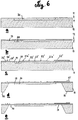
- Fig. 6 shows a modified method of that just explained for the method of fig. 5.
- Steps of figs. 6a and 6b are the same as for figs. 5a and 5b.
- the excitation resistors 21a', 21b', 22', the piezoresistor 32' and the passive resistor 33' are made from deposition of thin film-resistances in a manner known to any expert in the art.
- conductor films 52' and 56' are deposited in a manner known to any expert in the art, the exact dimensions of the resistors and conductors being determined through conventional etching process.
- a similar etching process as that explained for figures 5d and 5e is carried out.
- Fig. 7 is a variant of the embodiment of fig. 4, the basic difference being that excitation is created at one of the springs 31 and detection is made at the other spring 30.
- Electronic circuitry 70 is provided to connect to an excitation assembly 97 and a detection assembly 92.
- the excitation assembly shown in the high level block electronic circuit of fig. 7 includes two resistors 98 and 99, either of diffused or deposited, thin-film type resistors.
- the resistors 98 and 99 have a common connection to contact area 72 via interconnection line 75.
- Resistor 98 connects with contact area 71 via interconnection line 74.
- Resistor 99 connects with contact area 73 via interconnection line 76.
- the electronic circuitry 70 connects with contact areas 71, 72 and 73 via respective wires 77, 78 and 79 to provide resistors 98 and 99 selectively with pulsating current to create a vibration mode in the beam mass 20, said vibration mode detectable by assembly 92.
- the detection assembly 92 has piezoresistors 93-96 connected in a Wheatstone bridge fashion and in contact with contact areas 80, 81, 82 and 83 via interconnection lines 84-87. Further, the contact areas 80, 81, 82 and 83 are interconnected with the electronic circuitry 70 via wires 88, 89, 90 and 91, respectively.
- piezo-resistor assembly 92 a Wheatstone bridge structure is provided in the piezo-resistor assembly 92.
- the piezo-resistors 93 and 95 are transversal resistors, and the piezoresistors 94 and 96 are longitudinal resistors.
- a detector couple like piezo resistors 32 and 33 of fig. 4 could be envisaged in an alternative of the invention as shown in fig. 7.
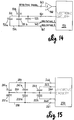
- the electronic circuitry 70 as well as corresponding circuitry 40 of fig. 4, circuitry 170 of fig. 14, or circuitry 270 of fig. 15 are all capable of producing alternating or pulsed excitation signal in electrical current or voltage form, and further have means for detecting changes in detector output as a result of applied forces to the beam mass 20.
- the specific means for producing such excitation signals as well as detecting detector output and any changes in detector output are all of a type well familiar to an expert in the art.
- fig. 1 and resonant mode 9 of fig. 3 can be realized by using electrostatic force as excitation mode and capacitance change as detection mode, with reference to a third detailed embodiment shown in fig. .
- This embodiment is based on the same type of silicon substrate 15 with the same flexible and electrically conductive mass 20 suspended by the two flexible and conductive springs 30 and 31 at opposite sides of the mass, these springs being fixed to the rigid frame 16 of the substrate 15.
- An undoped semi-insulating poly-silicon lid 110 is built over the area of the mass 20 and the springs 30 and 31 at a short distance therefrom, supported by and resting on the frame 16 and covered by an insulating layer (not shown).
- a cross-section Y10-Y11 is made through the lid 110 along planes perpendicular to the plane of the surface of the mass 20 and springs 30, 31 showing excitation electrodes 121a, 121b and 122 for enforcing vibration mode 9 and electrode 132 to act as a detector capacitor.
- These electrodes and their interconnection lines 151, 152 and 153 are made on the bottom side surface of the poly-silicon lid as doped low-ohmic poly-silicon conductors or hightemperature resistance thin-film metal such as tungsten with pattern as shown in fig. 8. These lines 151-153 connect with respective electrical contact areas 161, 162 and 163. Electrodes 121a and 121b are interconnected by conductor 154.
- the N-type doped electrical conductive mass 20 and springs 30 and 31 can be connected via the contact area 160 and form a common electrode for the excitation electrodes 121a, 121b, 122 and also form the second electrode for the detection capacitor with its first electrode 132.
- Electronic 170 circuitry (as will be explained in connection with fig. 14) can then be coupled to the device of this embodiment by electrical connections through the contact areas 160, 161, 162 and 163 in a similar way as given in the example of fig. 4.
- Excitation of resonant mode 9 can now be done by applying voltage pulses to the excitation electrodes at a frequency equivalent to the resonance frequency of resonant mode 9.
- Electrode 122 is pulsed with voltage pulses 180 degree phase shifted compared to the voltage pulses applied to electrodes 121a and 121b.
- the electric field between the electrodes and the mass will set up electrostatic forces between the electrodes and the mass, thereby causing a bending of the mass in the direction of the electrical field, and thereby enforcing vibrations in the mass-spring system at the frequency of vibration mode 9.
- the acceleration sensitivity is defined by the mechanical dimensions and the elastic properties of silicon only and not by the electrical parts, the sensitivity of this embodiment will be the same as for the embodiment of fig. 2 with the same mechanical dimensions of the mass-spring system.
- the detailed embodiment of force transducer according to fig. 8 can be manufactured by using conventional silicon wafer processing method and silicon micromachining technology.
- the processing method is more fully understood by reference to fig. 10, and with further reference to cross-section Y10-Y11 of fig. 8.
- Fig. 11f shows the cross-sectional view Y10-Y11 of fig. 8 .
- Processing is started on a ⁇ 1-0-0 ⁇ P-type silicon substrate 15 as for the embodiment of fig. 4.
- the result of the first two main steps are shown on fig. 10a and are to form the thickness T1 of the mass and the thickness T2 of the springs as N-type areas to make possible selective etching of the P-type silicon and stop the etch against the PN-junction at a later step in the process sequence.
- the pattern of the mass 20 is defined, doped by ion implantation and diffused to the correct depth corresponding to mass thickness T1 and then followed by an additional fotoetching and doping step for the pattern of the springs but leaving undoped P-areas around the mass and along the sides of the springs to allow at a later stage the complete mass-spring system to be etched to the original surface of the substrate 15 by etch-stop against PN-junction process.
- a pattern of oxide 150 with high etch-rate in hydrofluoric acid is deposited by low-temperature vapour deposition (LTO) and formed by standard photoetching techniques to be used as a sacrificial layer at a later stage in the process sequence.
- LTO low-temperature vapour deposition
- fig. 10c the electrically conductive poly-silicon or tungsten electrodes 121a, 121b, 122, 132 as well as the complete interconnection pattern of fig. 8 including all the interconnection lines 151, 152, 153 and 154 of which only lines 151 and 152 appear in section Y10-Y11 of fig. 8.
- the semi-insulating undoped poly-silicon material for the lid is deposited and formed over the sacrificial layer 150, the electrodes and the support frame for the lid 111. Holes are formed in this semi-insulating poly-silicon at the areas of the electrical contacts regions 160, 161, 162 and 163.
- 10d and 10e are now to form aluminium electrical contacts 170, 171,172, 173 onto the contact regions 160, 161, 162 , 163 (only contact 170 has been shown with corresponding region 160) and performing the etch-stop process to remove P-type silicon all the way to the PN-junction in the substrate around the mass 20 and the springs 30,31 by using an etchmask 180.
- the P-type silicon is removed around the mass 20 and along the sides of the springs 30, 31 leaving and exposing the sacrificial layer 150 at these areas.
- the last step as shown in fig.
- the sacrificial oxide layer 150 is removed in hydrofluoric acid HF by masking the front side of the wafer with its metal with a polyimide which is removed after the completion of the etching of the sacrificial layer 150.
- This detailed embodiment can now be built into a system including proper electronic circuitry that is needed to drive and keep the mass-spring system in its resonance mode and to condition the electrical output signal.
- fig. 1 and resonant mode of fig. 3 will now be further described in relation to the embodiment of fig. 11, i. e. by using electrostatic force as excitation mode and capacitance change as detection mode, thus describing a fourth detailed embodiment of the invention.
- This embodiment utilizes a different method by using poly-silicon material in the flexible mass and in the springs. This method allow the embodiment to be integrated with electronic circuitry on a single chip by adding extra process steps to an integrated circuit process, but can also be built as a separate sensor chip with associated electronic circuitry connected thereto.
- a flexible and electrically conductive mass 220 is suspended by means of two flexible, electrically and conductive springs 230 and 231 at opposite sides of the mass.
- the mass-spring system is provided with air space adjacent both surfaces thereof to be freely suspended between the substrate 215 and a lid 210.
- the lid 210 is made of undoped semi-insulating poly-silicon with different sections 210a, 210b and 210c built over and at a short distance from the mass 220 and the springs 230 and 231 and supportedly and resting on the substrate 215 with its anchor area 216.
- the cross-section Y20-Y21 is made through the lid 210 along planes perpendicular to the surface plane of the mass and springs.
- the substrate supports excitation electrodes 221a and 221b coupled together by interconnection line 254 and excitation electrode 222 for enforcing the vibration mode illustrated in fig. 3 by means of electrostatic force over the narrow air gap provided between these electrodes and the mass-spring system 220, 230, 231.
- These electrodes and their interconnection lines 251, 252 and 253 as also shown in fig. 12a are made on the surface of the substrate 215 and placed at the area of maximum deflection of the mass 220 for the resonant mode shown in fig. 3.
- Capacitive plates 241a and 241b and 242 are located on the bottom surface of an uppermost located midsection 210a of the lid 210 and form with the electrically conductive mass 220 capacitors with variable capacitance values, the mass 220, thus forming a single counter electrode and the air gap between the mid section 210a and the mass forming the dielectric of the capacitors thus created.
- the single common electrode created by the mass 220 is electrically connected to contact area 260 via spring 230, contact area 217 and interconnection line 250.
- the pattern of the capacitance plates 241a, 241b coupled together with interconnection line 259 and plate 242 with interconnection lines 253 and 254 to electrical connection and wire bonding areas 263 and 264 are shown in fig. 12b.
- the electrode and interconnections pattern of fig. 12a and fig. 12b are most effectively made of doped conductive poly-silicon.
- Electrical circuitry 270 (as explained further in connection with figure 15) can now be coupled to this mass-spring system by electrical connections to the contact areas 260, 261, 262, 263 and 264 in a similar way as given in the example of fig. 5.
- Excitation of resonant mode according to fig. 3 for this third embodiment according to fig. 11 can now be done by voltage pulses to the excitation electrodes 221a, 221b, 222 at a frequency equivalent to the resonant mode frequency.
- Electrode 222 is pulsed with voltage pulses 180 degree phase shifted relative to the voltage pulses applied to electrodes 221a and 221b.
- the electric field between the electrodes 221a, 221b and 2222 and the mass 220 will set up electrostatic forces between these electrodes and the mass 220 and cause a bending of the mass in the direction of the electrical field hereby enforcing the vibrations in the mass-spring system 220, 230, 231, at the vibration mode frequency according to fig. 3.
- the acceleration sensitivity of this fourth embodiment is defined by the mechanical dimensions and the elastic properties of the poly-silicon mass-spring system only and not by the electrical parts included therein.
- the force transducer of fig. 11 can be manufactured by using conventional silicon wafer processing method and surface micromachining by using sacrificial layers, as exemplified in fig. 13.
- Fig. 13 shows a cross-sectional view along planes denoted by line Y20-Y21 in fig. 9.
- Fig. 13 thus shows the main process steps that are used. Processing is started on a silicon substrate 215 with a passivation layer 211 on top as shown in fig. 13a.
- the substrate 215 could possibly contain all or parts of electronic circuitry to start and maintain the mass-spring system in its resonant mode and other signal conditioning circuitry to be used together with this embodiment of the invention.
- the pattern of the excitation electrodes 221a, 221b and 222 and their interconnection lines are formed in a layer of doped poly-silicon.
- the first sacrificial oxide layer 280 is deposited by chemical vapour deposition and formed by standard photoetching techniques in the area covered by the lid parts 210a and 210b shown in fig. 11.
- the shape or pattern of the springs 230 and 231 with their anchor areas 217 and 218 is formed by deposition of a thin layer of poly-silicon and photoetching this layer followed by an additional deposition of a thicker conductive polysilicon layer to form the mass 220 of the resonating mass-spring system.
- the poly-silicon mass and springs may also be made by depositing and etching the mass first and the springs and their support areas thereafter.
- a second sacrificial layer 281 is thereafter deposited and formed as shown in fig. 13d at the area covered by the lid parts 210a, 210b and 210c of fig. 11.
- the capacitor plates 241a, 241b and 242 and their respective interconnection lines as shown in fig.
- the present embodiment is now completed leaving air volumes 290 and 291 around the mass-spring system 220, 230, 231, thus providing a suspended system with the spring 230 effectively anchored to the substrate 215 at anchor area 217, spring 231 anchored to the substrate at anchor area 218 and with the thin flexible mass 220 free to move in the z-direction, i.e. right angles to the substrate, that direction being the sensing direction of the present embodiment.
- Fig. 14 shows a high level electronic circuit diagram to be used for the embodiment of fig. 8.
- Excitation voltage signals are supplied from the electronic circuitry 170 via contact areas 160, 161 and 162 to the electrodes of the first capacitor 121a and the electrodes of the second capacitors 121b 180 degrees out of phase with the excitation signal supplied to electrodes of the third capacitor 122. Movement of the mass 20 will lead to a change in the distance between the end of the mass and the electrode of the detection capacitor 132, resulting in capacitance change with the same frequency as applied mechanical vibration.
- the signal from the capacitor 132 is fed into a charge amplifier180 via contact area 163 and then to the electronic circuitry 170 built as a self oscillating loop or a phase locked loop.
- Fig. 15 shows a high level electronic circuit diagram to be used for the embodiment of fig. 11.
- Excitation voltage signals from the electronic circuitry 270 via contact areas 260, 261 and 262 are supplied to the electrodes of the first capacitor 221a and the electrode of the second capacitors 221b 180 degrees out of phase with the excitation signal supplied to electrode of the third capacitor 222.
- the resonant vibrations in the mass-spring system will lead to a deflection along the mass 20 as shown in fig. 3b leading to a time variable change in the distance between the mass 20 and the opposite electrode of capacitors 241a, 241b and 242 with signal on capacitor 242 180 degrees out of phase with signal on capacitors 241a and 241b.
- the signals from the detection capacitors 241a, 241b and 242 are fed into the electronic circuitry 270 via contact areas 260, 263 and 264 that is built as a self oscillating loop or a phase locked loop.
- the invention provides a defined resonant vibrational mode in the entire force sensitive mass-spring system in such a way that the proof mass is thin enough to flex or/and twist.
- a resonant mode is thus set up as an "integrated" movement of the spring and the mass. Acceleration or fluidic pressure force will change the mechanical stress and the stiffness of the springs and the mass and hereby causing a change of the resonance frequency of the mass-spring system.
- the proof mass has a thickness so that it effectively acts as a rigid body, then vibrations are set up by translational or/and rotational movement of the proof mass interactively with the springs flexing and/or twisting. Acceleration or other external sources of force will change the stress in the springs hereby causing a change in the stiffness of the springs resulting in a change in the resonance frequency of the enforced vibrational mode.
- the seismic mass-spring system itself is by design identically the same as the vibrating mass-spring system that is set into and held in a resonant mode having low damping (high Q-factor).
Landscapes
- Physics & Mathematics (AREA)
- Remote Sensing (AREA)
- Life Sciences & Earth Sciences (AREA)
- Engineering & Computer Science (AREA)
- General Physics & Mathematics (AREA)
- Acoustics & Sound (AREA)
- Geology (AREA)
- General Life Sciences & Earth Sciences (AREA)
- Environmental & Geological Engineering (AREA)
- Geophysics (AREA)
- Measuring Fluid Pressure (AREA)
- Micromachines (AREA)
- Steering Control In Accordance With Driving Conditions (AREA)
- Air Bags (AREA)
- Push-Button Switches (AREA)
- Pressure Sensors (AREA)
Applications Claiming Priority (2)
| Application Number | Priority Date | Filing Date | Title |
|---|---|---|---|
| US42167395A | 1995-04-12 | 1995-04-12 | |
| US421673 | 1995-04-12 |
Publications (2)
| Publication Number | Publication Date |
|---|---|
| EP0737864A1 true EP0737864A1 (fr) | 1996-10-16 |
| EP0737864B1 EP0737864B1 (fr) | 2000-08-30 |
Family
ID=23671552
Family Applications (1)
| Application Number | Title | Priority Date | Filing Date |
|---|---|---|---|
| EP96850074A Expired - Lifetime EP0737864B1 (fr) | 1995-04-12 | 1996-04-11 | Capteur de force |
Country Status (5)
| Country | Link |
|---|---|
| EP (1) | EP0737864B1 (fr) |
| JP (1) | JP3186975B2 (fr) |
| KR (1) | KR100239113B1 (fr) |
| AT (1) | ATE196012T1 (fr) |
| DE (1) | DE69610013T2 (fr) |
Cited By (4)
| Publication number | Priority date | Publication date | Assignee | Title |
|---|---|---|---|---|
| EP1923674A1 (fr) * | 2006-11-14 | 2008-05-21 | Infineon Technologies SensoNor AS | Capteur à rétrodiffusion modulé |
| RU2467296C1 (ru) * | 2011-07-26 | 2012-11-20 | Открытое акционерное общество "Авангард" | Силоизмерительное устройство |
| CN109850840A (zh) * | 2018-12-29 | 2019-06-07 | 杭州士兰集成电路有限公司 | Mems器件及其制造方法 |
| WO2024221967A1 (fr) * | 2023-04-28 | 2024-10-31 | 润芯感知科技(南昌)有限公司 | Dispositif à semi-conducteurs et son procédé de fabrication |
Families Citing this family (3)
| Publication number | Priority date | Publication date | Assignee | Title |
|---|---|---|---|---|
| JP4522143B2 (ja) * | 2004-05-20 | 2010-08-11 | キヤノン株式会社 | 真空計 |
| FR2917731B1 (fr) * | 2007-06-25 | 2009-10-23 | Commissariat Energie Atomique | Dispositif resonant a detection piezoresistive realise en technologies de surface |
| CN111654993B (zh) * | 2020-05-22 | 2021-11-05 | 中国航空工业集团公司西安航空计算技术研究所 | 一种模块等质量变刚度方法及等质量变刚度模块 |
Citations (4)
| Publication number | Priority date | Publication date | Assignee | Title |
|---|---|---|---|---|
| GB1596982A (en) * | 1978-02-21 | 1981-09-03 | Standard Telephones Cables Ltd | Mechanical resonator arrangements |
| US4805456A (en) * | 1987-05-19 | 1989-02-21 | Massachusetts Institute Of Technology | Resonant accelerometer |
| DE3814952A1 (de) * | 1988-05-03 | 1989-11-23 | Bosch Gmbh Robert | Sensor |
| EP0614087A2 (fr) * | 1993-03-01 | 1994-09-07 | Murata Manufacturing Co., Ltd. | Vibrateur piézoélectrique et capteur d'accélération utilisant ce vibrateur |
Family Cites Families (2)
| Publication number | Priority date | Publication date | Assignee | Title |
|---|---|---|---|---|
| GB2215053B (en) | 1988-02-13 | 1991-09-11 | Stc Plc | Transducer device |
| FR2720509B1 (fr) | 1994-05-27 | 1996-08-23 | Sextant Avionique | Microaccéléromètre à résonateur compensé en température. |
-
1996
- 1996-04-11 DE DE69610013T patent/DE69610013T2/de not_active Expired - Lifetime
- 1996-04-11 EP EP96850074A patent/EP0737864B1/fr not_active Expired - Lifetime
- 1996-04-11 JP JP11300096A patent/JP3186975B2/ja not_active Expired - Fee Related
- 1996-04-11 AT AT96850074T patent/ATE196012T1/de not_active IP Right Cessation
- 1996-04-12 KR KR1019960010947A patent/KR100239113B1/ko not_active Expired - Fee Related
Patent Citations (4)
| Publication number | Priority date | Publication date | Assignee | Title |
|---|---|---|---|---|
| GB1596982A (en) * | 1978-02-21 | 1981-09-03 | Standard Telephones Cables Ltd | Mechanical resonator arrangements |
| US4805456A (en) * | 1987-05-19 | 1989-02-21 | Massachusetts Institute Of Technology | Resonant accelerometer |
| DE3814952A1 (de) * | 1988-05-03 | 1989-11-23 | Bosch Gmbh Robert | Sensor |
| EP0614087A2 (fr) * | 1993-03-01 | 1994-09-07 | Murata Manufacturing Co., Ltd. | Vibrateur piézoélectrique et capteur d'accélération utilisant ce vibrateur |
Non-Patent Citations (1)
| Title |
|---|
| SATCHELL D W ET AL: "A THERMALLY-EXCITED SILICON ACCELEROMETER", SENSORS AND ACTUATORS, vol. 17, no. 1/02, 3 May 1989 (1989-05-03), pages 241 - 245, XP000118930 * |
Cited By (5)
| Publication number | Priority date | Publication date | Assignee | Title |
|---|---|---|---|---|
| EP1923674A1 (fr) * | 2006-11-14 | 2008-05-21 | Infineon Technologies SensoNor AS | Capteur à rétrodiffusion modulé |
| US7692358B2 (en) | 2006-11-14 | 2010-04-06 | Infineon Technologies Sensonor As | Backscatter sensor |
| RU2467296C1 (ru) * | 2011-07-26 | 2012-11-20 | Открытое акционерное общество "Авангард" | Силоизмерительное устройство |
| CN109850840A (zh) * | 2018-12-29 | 2019-06-07 | 杭州士兰集成电路有限公司 | Mems器件及其制造方法 |
| WO2024221967A1 (fr) * | 2023-04-28 | 2024-10-31 | 润芯感知科技(南昌)有限公司 | Dispositif à semi-conducteurs et son procédé de fabrication |
Also Published As
| Publication number | Publication date |
|---|---|
| KR100239113B1 (ko) | 2000-01-15 |
| DE69610013D1 (de) | 2000-10-05 |
| ATE196012T1 (de) | 2000-09-15 |
| EP0737864B1 (fr) | 2000-08-30 |
| JPH08292207A (ja) | 1996-11-05 |
| DE69610013T2 (de) | 2001-01-11 |
| JP3186975B2 (ja) | 2001-07-11 |
Similar Documents
| Publication | Publication Date | Title |
|---|---|---|
| US5834646A (en) | Force sensor device | |
| EP0391512B1 (fr) | Palpeur de force gravé au silicium et son procédé de fabrication | |
| US5233874A (en) | Active microaccelerometer | |
| US8156807B2 (en) | Piezo-resistive detection resonant device made using surface technologies | |
| US10036764B2 (en) | Bulk acoustic wave accelerometers | |
| JP4871513B2 (ja) | 薄く形成されたカンチレバー構造を備えた微小機械装置及び関連の方法 | |
| US4901570A (en) | Resonant-bridge two axis microaccelerometer | |
| JP5016747B2 (ja) | 機械的応力に対して不感受性であるマイクロ電気機械構造体 | |
| US6199874B1 (en) | Microelectromechanical accelerometer for automotive applications | |
| US6286369B1 (en) | Single-side microelectromechanical capacitive acclerometer and method of making same | |
| US6149190A (en) | Micromechanical accelerometer for automotive applications | |
| US8047075B2 (en) | Vertically integrated 3-axis MEMS accelerometer with electronics | |
| US4945765A (en) | Silicon micromachined accelerometer | |
| US5767405A (en) | Comb-drive micromechanical tuning fork gyroscope with piezoelectric readout | |
| US6718605B2 (en) | Single-side microelectromechanical capacitive accelerometer and method of making same | |
| US6487864B1 (en) | Cyrogenic inertial micro-electro-mechanical system (MEMS) device | |
| CN107003333B (zh) | Mems传感器和半导体封装 | |
| US5045152A (en) | Force transducer etched from silicon | |
| JPH0832090A (ja) | 慣性力センサおよびその製造方法 | |
| JP2004245760A (ja) | 圧力と加速度との双方を検出するセンサおよびその製造方法 | |
| EP0737864B1 (fr) | Capteur de force | |
| US5461918A (en) | Vibrating beam accelerometer | |
| JP2001133479A (ja) | 慣性力センサおよびその製造方法 | |
| JP3333285B2 (ja) | 半導体センサ | |
| JP3421340B2 (ja) | 強誘電薄膜進行波回転センサ |
Legal Events
| Date | Code | Title | Description |
|---|---|---|---|
| PUAI | Public reference made under article 153(3) epc to a published international application that has entered the european phase |
Free format text: ORIGINAL CODE: 0009012 |
|
| AK | Designated contracting states |
Kind code of ref document: A1 Designated state(s): AT BE CH DE DK ES FI FR GB GR IE IT LI LU MC NL PT SE |
|
| 17P | Request for examination filed |
Effective date: 19960913 |
|
| 17Q | First examination report despatched |
Effective date: 19990211 |
|
| GRAG | Despatch of communication of intention to grant |
Free format text: ORIGINAL CODE: EPIDOS AGRA |
|
| GRAG | Despatch of communication of intention to grant |
Free format text: ORIGINAL CODE: EPIDOS AGRA |
|
| GRAG | Despatch of communication of intention to grant |
Free format text: ORIGINAL CODE: EPIDOS AGRA |
|
| GRAH | Despatch of communication of intention to grant a patent |
Free format text: ORIGINAL CODE: EPIDOS IGRA |
|
| RAP1 | Party data changed (applicant data changed or rights of an application transferred) |
Owner name: SENSONOR ASA |
|
| GRAH | Despatch of communication of intention to grant a patent |
Free format text: ORIGINAL CODE: EPIDOS IGRA |
|
| GRAA | (expected) grant |
Free format text: ORIGINAL CODE: 0009210 |
|
| AK | Designated contracting states |
Kind code of ref document: B1 Designated state(s): AT BE CH DE DK ES FI FR GB GR IE IT LI LU MC NL PT SE |
|
| PG25 | Lapsed in a contracting state [announced via postgrant information from national office to epo] |
Ref country code: NL Free format text: LAPSE BECAUSE OF FAILURE TO SUBMIT A TRANSLATION OF THE DESCRIPTION OR TO PAY THE FEE WITHIN THE PRESCRIBED TIME-LIMIT Effective date: 20000830 Ref country code: LI Free format text: LAPSE BECAUSE OF FAILURE TO SUBMIT A TRANSLATION OF THE DESCRIPTION OR TO PAY THE FEE WITHIN THE PRESCRIBED TIME-LIMIT Effective date: 20000830 Ref country code: IT Free format text: LAPSE BECAUSE OF FAILURE TO SUBMIT A TRANSLATION OF THE DESCRIPTION OR TO PAY THE FEE WITHIN THE PRESCRIBED TIME-LIMIT;WARNING: LAPSES OF ITALIAN PATENTS WITH EFFECTIVE DATE BEFORE 2007 MAY HAVE OCCURRED AT ANY TIME BEFORE 2007. THE CORRECT EFFECTIVE DATE MAY BE DIFFERENT FROM THE ONE RECORDED. Effective date: 20000830 Ref country code: GR Free format text: LAPSE BECAUSE OF NON-PAYMENT OF DUE FEES Effective date: 20000830 Ref country code: FI Free format text: LAPSE BECAUSE OF FAILURE TO SUBMIT A TRANSLATION OF THE DESCRIPTION OR TO PAY THE FEE WITHIN THE PRESCRIBED TIME-LIMIT Effective date: 20000830 Ref country code: ES Free format text: THE PATENT HAS BEEN ANNULLED BY A DECISION OF A NATIONAL AUTHORITY Effective date: 20000830 Ref country code: CH Free format text: LAPSE BECAUSE OF FAILURE TO SUBMIT A TRANSLATION OF THE DESCRIPTION OR TO PAY THE FEE WITHIN THE PRESCRIBED TIME-LIMIT Effective date: 20000830 Ref country code: BE Free format text: LAPSE BECAUSE OF FAILURE TO SUBMIT A TRANSLATION OF THE DESCRIPTION OR TO PAY THE FEE WITHIN THE PRESCRIBED TIME-LIMIT Effective date: 20000830 Ref country code: AT Free format text: LAPSE BECAUSE OF FAILURE TO SUBMIT A TRANSLATION OF THE DESCRIPTION OR TO PAY THE FEE WITHIN THE PRESCRIBED TIME-LIMIT Effective date: 20000830 |
|
| REF | Corresponds to: |
Ref document number: 196012 Country of ref document: AT Date of ref document: 20000915 Kind code of ref document: T |
|
| REG | Reference to a national code |
Ref country code: CH Ref legal event code: EP |
|
| REG | Reference to a national code |
Ref country code: IE Ref legal event code: FG4D |
|
| REF | Corresponds to: |
Ref document number: 69610013 Country of ref document: DE Date of ref document: 20001005 |
|
| ET | Fr: translation filed | ||
| PG25 | Lapsed in a contracting state [announced via postgrant information from national office to epo] |
Ref country code: SE Free format text: LAPSE BECAUSE OF FAILURE TO SUBMIT A TRANSLATION OF THE DESCRIPTION OR TO PAY THE FEE WITHIN THE PRESCRIBED TIME-LIMIT Effective date: 20001130 Ref country code: PT Free format text: LAPSE BECAUSE OF FAILURE TO SUBMIT A TRANSLATION OF THE DESCRIPTION OR TO PAY THE FEE WITHIN THE PRESCRIBED TIME-LIMIT Effective date: 20001130 Ref country code: DK Free format text: LAPSE BECAUSE OF FAILURE TO SUBMIT A TRANSLATION OF THE DESCRIPTION OR TO PAY THE FEE WITHIN THE PRESCRIBED TIME-LIMIT Effective date: 20001130 |
|
| NLV1 | Nl: lapsed or annulled due to failure to fulfill the requirements of art. 29p and 29m of the patents act | ||
| REG | Reference to a national code |
Ref country code: CH Ref legal event code: PL |
|
| PG25 | Lapsed in a contracting state [announced via postgrant information from national office to epo] |
Ref country code: LU Free format text: LAPSE BECAUSE OF NON-PAYMENT OF DUE FEES Effective date: 20010411 Ref country code: IE Free format text: LAPSE BECAUSE OF NON-PAYMENT OF DUE FEES Effective date: 20010411 |
|
| PG25 | Lapsed in a contracting state [announced via postgrant information from national office to epo] |
Ref country code: MC Free format text: LAPSE BECAUSE OF NON-PAYMENT OF DUE FEES Effective date: 20010430 |
|
| PLBE | No opposition filed within time limit |
Free format text: ORIGINAL CODE: 0009261 |
|
| STAA | Information on the status of an ep patent application or granted ep patent |
Free format text: STATUS: NO OPPOSITION FILED WITHIN TIME LIMIT |
|
| 26N | No opposition filed | ||
| REG | Reference to a national code |
Ref country code: GB Ref legal event code: IF02 |
|
| REG | Reference to a national code |
Ref country code: IE Ref legal event code: MM4A |
|
| PGFP | Annual fee paid to national office [announced via postgrant information from national office to epo] |
Ref country code: GB Payment date: 20030320 Year of fee payment: 8 |
|
| PGFP | Annual fee paid to national office [announced via postgrant information from national office to epo] |
Ref country code: FR Payment date: 20040408 Year of fee payment: 9 |
|
| PG25 | Lapsed in a contracting state [announced via postgrant information from national office to epo] |
Ref country code: GB Free format text: LAPSE BECAUSE OF NON-PAYMENT OF DUE FEES Effective date: 20040411 |
|
| GBPC | Gb: european patent ceased through non-payment of renewal fee |
Effective date: 20040411 |
|
| PG25 | Lapsed in a contracting state [announced via postgrant information from national office to epo] |
Ref country code: FR Free format text: LAPSE BECAUSE OF NON-PAYMENT OF DUE FEES Effective date: 20051230 |
|
| REG | Reference to a national code |
Ref country code: FR Ref legal event code: ST Effective date: 20051230 |
|
| REG | Reference to a national code |
Ref country code: DE Ref legal event code: R082 Ref document number: 69610013 Country of ref document: DE Representative=s name: COHAUSZ & FLORACK PATENT- UND RECHTSANWAELTE P, DE |
|
| REG | Reference to a national code |
Ref country code: DE Ref legal event code: R082 Ref document number: 69610013 Country of ref document: DE Representative=s name: COHAUSZ & FLORACK PATENT- UND RECHTSANWAELTE P, DE Effective date: 20111012 Ref country code: DE Ref legal event code: R081 Ref document number: 69610013 Country of ref document: DE Owner name: INFINEON TECHNOLOGIES AG, DE Free format text: FORMER OWNER: SENSONOR ASA, HORTEN, NO Effective date: 20111012 |
|
| PGFP | Annual fee paid to national office [announced via postgrant information from national office to epo] |
Ref country code: DE Payment date: 20150616 Year of fee payment: 20 |
|
| REG | Reference to a national code |
Ref country code: DE Ref legal event code: R071 Ref document number: 69610013 Country of ref document: DE |