EP0750389A2 - Convertisseur - Google Patents
Convertisseur Download PDFInfo
- Publication number
- EP0750389A2 EP0750389A2 EP96109795A EP96109795A EP0750389A2 EP 0750389 A2 EP0750389 A2 EP 0750389A2 EP 96109795 A EP96109795 A EP 96109795A EP 96109795 A EP96109795 A EP 96109795A EP 0750389 A2 EP0750389 A2 EP 0750389A2
- Authority
- EP
- European Patent Office
- Prior art keywords
- pulse
- converter
- control signal
- circuit
- voltage
- Prior art date
- Legal status (The legal status is an assumption and is not a legal conclusion. Google has not performed a legal analysis and makes no representation as to the accuracy of the status listed.)
- Granted
Links
Images


Classifications
-
- H—ELECTRICITY
- H02—GENERATION; CONVERSION OR DISTRIBUTION OF ELECTRIC POWER
- H02M—APPARATUS FOR CONVERSION BETWEEN AC AND AC, BETWEEN AC AND DC, OR BETWEEN DC AND DC, AND FOR USE WITH MAINS OR SIMILAR POWER SUPPLY SYSTEMS; CONVERSION OF DC OR AC INPUT POWER INTO SURGE OUTPUT POWER; CONTROL OR REGULATION THEREOF
- H02M3/00—Conversion of DC power input into DC power output
- H02M3/22—Conversion of DC power input into DC power output with intermediate conversion into AC
- H02M3/24—Conversion of DC power input into DC power output with intermediate conversion into AC by static converters
- H02M3/28—Conversion of DC power input into DC power output with intermediate conversion into AC by static converters using discharge tubes with control electrode or semiconductor devices with control electrode to produce the intermediate AC
- H02M3/325—Conversion of DC power input into DC power output with intermediate conversion into AC by static converters using discharge tubes with control electrode or semiconductor devices with control electrode to produce the intermediate AC using devices of a triode or a transistor type requiring continuous application of a control signal
- H02M3/335—Conversion of DC power input into DC power output with intermediate conversion into AC by static converters using discharge tubes with control electrode or semiconductor devices with control electrode to produce the intermediate AC using devices of a triode or a transistor type requiring continuous application of a control signal using semiconductor devices only
- H02M3/33507—Conversion of DC power input into DC power output with intermediate conversion into AC by static converters using discharge tubes with control electrode or semiconductor devices with control electrode to produce the intermediate AC using devices of a triode or a transistor type requiring continuous application of a control signal using semiconductor devices only with automatic control of the output voltage or current, e.g. flyback converters
-
- H—ELECTRICITY
- H02—GENERATION; CONVERSION OR DISTRIBUTION OF ELECTRIC POWER
- H02M—APPARATUS FOR CONVERSION BETWEEN AC AND AC, BETWEEN AC AND DC, OR BETWEEN DC AND DC, AND FOR USE WITH MAINS OR SIMILAR POWER SUPPLY SYSTEMS; CONVERSION OF DC OR AC INPUT POWER INTO SURGE OUTPUT POWER; CONTROL OR REGULATION THEREOF
- H02M1/00—Details of apparatus for conversion
- H02M1/0003—Details of control, feedback or regulation circuits
- H02M1/0032—Control circuits allowing low power mode operation, e.g. in standby mode
-
- Y—GENERAL TAGGING OF NEW TECHNOLOGICAL DEVELOPMENTS; GENERAL TAGGING OF CROSS-SECTIONAL TECHNOLOGIES SPANNING OVER SEVERAL SECTIONS OF THE IPC; TECHNICAL SUBJECTS COVERED BY FORMER USPC CROSS-REFERENCE ART COLLECTIONS [XRACs] AND DIGESTS
- Y02—TECHNOLOGIES OR APPLICATIONS FOR MITIGATION OR ADAPTATION AGAINST CLIMATE CHANGE
- Y02B—CLIMATE CHANGE MITIGATION TECHNOLOGIES RELATED TO BUILDINGS, e.g. HOUSING, HOUSE APPLIANCES OR RELATED END-USER APPLICATIONS
- Y02B70/00—Technologies for an efficient end-user side electric power management and consumption
- Y02B70/10—Technologies improving the efficiency by using switched-mode power supplies [SMPS], i.e. efficient power electronics conversion e.g. power factor correction or reduction of losses in power supplies or efficient standby modes
Definitions
- Pulse-width modulated converters in particular direct current converters, operate in normal operation with a constant operating frequency.
- the output voltage of the converter is regulated by changing the pulse duty factor t on / T of the control signal for the electronic switch of the converter.
- this is compared, for example, with a specified voltage setpoint in an error amplifier.
- the error amplifier forwards the amplified control deviation to a control input of the pulse width modulator. This controls the pulse duty factor ton / T of the control signal at the output of the pulse width modulator for the electrical switch in accordance with the magnitude of the amplified control deviation.
- a current limiting circuit ensures a reduction in the clock ratio of the converter's electronic switch.
- This current limiting circuit measures, for example via a shunt (measuring resistor), the current flowing in the primary circuit of the converter and, after reaching a critical current threshold value, switches off the electronic switch prematurely.
- the measurement of the primary current and the switching off of the electronic switch have a delay time.
- the delay time is set, for example, by the switching times within a comparison unit, the signal runtime in the control IC, the time in which the output signal for the electronic switch is reset and the switching time that the electronic switch requires until it interrupts the primary circuit after the switch-off signal arrives , together.
- the minimum possible switch-on time t onmin results for the converter. Since the output voltage of the converter is determined by the ratio t on / T, it follows that in the case of a low-resistance short circuit, the switch-on time t on of the electronic switch must go to zero.
- the duty cycle t on / T must also be greatly reduced, since the transmitted power of the system is greater than the power demanded of the converter at the circuit output. For a given period T, a shorter switch-on time t on of the electronic switch is then required, which is shorter than the minimum possible switch-on time t onmin of the electronic switch of the converter. If the output voltage of the converter is above a specified voltage setpoint, the error amplifier also prevents the electronic switch from switching through again. The electronic switch is only switched on when the output voltage has dropped below the voltage setpoint again and is enabled again by the error amplifier.
- Such a circuit configuration of a converter is known for example from the German patent DE 28 38 009.
- inverters may be dimensioned for the corresponding output voltages.
- the specially dimensioned inverters are synchronized with each other.
- the advantages lie in the use of a uniform switching frequency.
- the AC load on the intermediate circuit capacitors is reduced by suitable phase selection of the converters, for example, operated in push-pull mode.
- a common end interference filter can be used for synchronized inverters. If the inverters are not operated synchronized, the working frequencies of the individual inverters would differ slightly due to the inevitable tolerances. This difference in the operating frequency affects the common voltage supply of the converter circuits as a beat. Since the repercussions on the voltage supply are subject to certain, defined limit values, disturbing frequencies must be kept away from the supply lines with appropriately dimensioned filters. Since the beat frequency corresponds to the difference frequencies of the individual inverters, the possible frequency spectrum starts at 0 Hz, making a filter dimension impossible. The converters would have to be individually suppressed in unsynchronized operation.
- the object of the invention is to design a converter in such a way that it can be operated at variable frequencies in the low-load or overload case and in normal operation at a constant operating frequency with pulse width modulation.
- the invention has the advantage that in normal operation the converter operates at a constant frequency and can be synchronized with other converters, while in the case of low load or overload the duty cycle is changed by a new period and thus reduces the operating frequency in the case of low load and short circuit and a further increase in the output voltage or the short-circuit current is prevented.
- the advantages of a frequency-variable converter in the case of light loads and overloads are combined with the advantages of a frequency-constant converter operated with pulse-width modulation.
- the converter works like a converter with a constant frequency and can be synchronized with other converters.
- the converter maintains its minimum duty cycle t onmin * , but changes the operating frequency according to the current or voltage conditions.
- an actuating signal is fed to the clock generator (VCO), as a result of which the clock frequency changes until a steady operating state is restored.
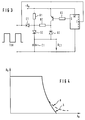
- FIG. 1 shows a circuit arrangement shown in the block diagram of a converter with a control module.
- This converter with control module essentially consists of the circuit module of a converter C, a pulse width modulator PWM, an error amplifier F and a clock generator whose frequency (VCO) can be changed and a detector circuit D which detects, for example, a short-circuit or overload case and accordingly over its output signal regulates the frequency of the clock generator (VCO).
- VCO clock generator
- the output signal of the monoflop MF is on the one hand at the connection terminals of the ratio generator V and on the other hand the control signal of the electronic switch is at a second input.
- the ratio generator is used to form the ratio between the duty cycle of the control signal t on to the duty cycle t onmin * of the output signal of the monoflop MF. This "ratio formation" is achieved by synchronous averaging of the signals listed above.
- the pulse width modulator PWM is controlled by a current flowing on the primary side in the measuring resistor of the main circuit and an output voltage applied to the converter on the secondary side influenced.
- the output signal of the pulse width modulator PWM determines the duty cycle of the electronic switch of the converter C.
- This output signal which is present at the output terminals PG of the pulse width modulator PWM and whose pulse width is influenced by the measured values determined on the primary or secondary side at the transformer of the converter, is at the input of the detector circuit D.
- the control signal t on for the electronic switch triggers the monoflop MF arranged in the detector circuit D.
- This monoflop MF generates a defined time window for the synchronous averaging.
- the pulse length of the output signal of the monoflop t onmin * defines the switch-on time from which the converter works frequency-modulated.
- the converter In this operating phase, the converter is operated with a constant switch-on time t on , but with a variable frequency.
- the mode of operation of the detector circuit D is shown in FIG. 2 on the basis of pulse diagrams and explained on the basis of the circuit structure shown in FIG.
- the operating point of the converter is recognized by the detector circuit D, from which the output current begins to rise in an uncontrolled manner.
- the increase in the output current occurs at the minimum possible switch-on time t onmin , since the duty cycle is due to the delay times cannot be reduced further.
- the detector circuit D prevents the converter from reaching this shortest possible on-time t onmin .
- the current switch-on time t on is measured.
- the effective pulse duty factor t on / T neu is thus reduced without the switch-on time ton having to be shortened.
- the constant switch-on time t onmin * of the MF is preferably slightly above t onmin .
- the ratio t on / t onmin * of the current duty cycle t on to the defined minimum duty cycle t onmin * is converted into a voltage proportional to this duty cycle.
- FIG. 2 shows pulse diagrams 2A to 2F to explain the circuit arrangement shown in FIG.
- Line 2A shows the control signal t on , which controls the electronic switch of the converter in accordance with pulse width modulation by the pulse width modulator PWM.
- Line 2B shows the output signal of the monostable multivibrator MF. Due to an increasing overload or relief at the output of the converter, the switch-on time t on or the pulse width of the control signal is continuously reduced. From a certain point in time, here t on ⁇ t onmin * , the frequency of the clock generator is reduced.
- FIG. 2C shows the charging time or, in line 2D, the discharging time of a capacitor C1 arranged in the comparator V of the detector circuit D.
- the capacitor C1 is discharged, as indicated in line 2D, when the pulse width of the control signal falls below the pulse width of the output signal output by the monoflop MF.
- the logic of the detector circuit D is also reproduced in a certain way in line 2E: If the pulse width ton of the control signal is greater than the pulse width t onmin * of the monoflop MF, the capacitor C1 is charged during the "low" signal at the output of the monoflop MF held. The pulse width of the control signal smaller than the pulse width of the monoflop MF, the charging time of the capacitor is shortened accordingly.
- the capacitor C1 discharges during the time difference t onmin * - t on (see line 2D).
- the control signal present at capacitor C1 is shown in line 2F.
- the maximum possible voltage across R1 is present across capacitor C1. If the pulse duration of the monoflop MF falls below the pulse duration of the control signal, the capacitor C1 is discharged accordingly via R2.
- the voltage U C1 controlling the clock generator (VCO) corresponds in each case to the ratio of the pulse widths t onmin * to t on .
- FIG. 3 shows a circuitry implementation of the detector circuit D. It is composed of the monoflop MF and the synchronous mean value image V.
- the drive signal t on which is emitted by the pulse width modulator PWM, is present.
- the control signal U C1 for the clock generator (VCO) is tapped at the capacitor C1.
- the monostable multivibrator MF is triggered at the same time. This emits a pulse of a certain pulse width at output Q. For example, transistor T1 is blocked during the high potential of the pulse.
- the charging circuit for the capacitor C1 is charged by the operating potential source designated U h via the resistor R1 and the diode D2.
- FIG. 4 shows the curve profiles marked a, b.
- the curve marked a occurs when, for example in the case of a low-impedance short circuit, the pulse duration of the control signal has to go to zero, but this is not possible due to the signal delays caused by technology and the output current continues to increase.
- the mode of operation of the detector circuit D and the output characteristic curve of a converter to be achieved thereby are shown in the curve profile marked b.
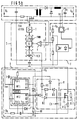
- FIG. 5a shows a circuit arrangement in connection with the control module TDA4916G from Siemens AG.
- a control circuit S (TDA 4916 G) is used to control the electronic switch of the converter C.
- the electronic switch is connected with its control electrode to the control output 4 of the control circuit S.
- the controller R is connected to the outputs b1, b2 of the converter.
- An opto-coupler, the photodiode of which is connected to the regulator R, is arranged between the regulator R and the control circuit S.
- the phototransistor of the opto-coupler is at the reference potential on the emitter side.
- the control circuit S also contains the clock generator G (expanded to a voltage-controlled oscillator (VCO) by the circuitry), to the output of which an arrangement consisting of a logic arrangement and the pulse width modulator is connected. This arrangement is controlled by a comparator K. Between the output of the pulse width modulator and the gate electrode of the electronic switch is a driver T, which outputs control pulses with a variable pulse duty factor at its output to the gate electrode of the electronic switch. Furthermore, a synchronization module SYN is present in the control circuit S, which influences the clock generator.
- VCO voltage-controlled oscillator
- the monoflop MF provided for the circuit arrangement D for generating the time t onmin * is realized with the components R3, R4, R5, T2 and C2.
- a "high" signal at the output 14 of the control circuit S drives the transistor T2 via the level adjustment R3 and R4, as a result of which C2 can discharge.
- the signal at the output 14 of the control circuit S is on "Low" potential leads, the transistor T2 is blocked and C2 can charge via R5.
- the voltage potential at the capacitor C2 is compared with a reference voltage source Uref via a differential amplifier consisting of R8, R9, R10, T3 and T4.
- the differential amplifier can also be designed as an operational amplifier or comparator.
- the reference voltage source U Ref can also be arranged in the control module S. Only as long as the potential at the capacitor C2 is less than the reference voltage U Ref can the synchronous mean value image V, consisting of R1, R2, D1, D2, D3, T1 and C1, work as described under FIG. 3.
- the resistor R7 effects a positive feedback of the differential amplifier and thus enables shorter switching times.
- the switching behavior is further improved by C3 or the anti-saturation diode D4. If the voltage potential at C2 reaches the level of the reference voltage, the transistor T3 of the differential amplifier switches through and the transistor T1 is also turned on, as a result of which the capacitor C1 of the synchronous mean value generator V can no longer discharge.
- the circuit thus maps the ratio V ⁇ t on / t onmin * at capacitor C1.
- the gain factor V can be adjusted by dimensioning R1 and R2.
- the control signal obtained at C1 controls the actuator T5, which determines the operating frequency of the control module S. Case 1: t on > t onmin *
- FIG. 5b shows a further circuit design of the block diagram shown in FIG. 1.
- the function of the circuit arrangement shown in FIG. 5b corresponds to the function of the circuit arrangement shown in FIG. 5a, the discrete monostable multivibrator MF being replaced by an integrated circuit (IC14528), here two independent monostable multivibrators MF1, MF2.
- IC14528 integrated circuit
- MF1 monostable multivibrators
- a monostable flip-flop is sufficient for the function of the circuit.
- the integrated circuit (IC 14528) causes a switching delay of the drive signal for the synchronous mean value V.
- the second monostable multivibrator MF2 is used in this integrated circuit for pulse processing.
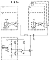
- FIG. 6a shows a circuit arrangement in which several converters C1,..., Cn work synchronously.
- one of the inverters here Cn
- it When one of the inverters (here Cn) changes from constant frequency to variable frequency operation, it must be disconnected from the common synchronization.
- FIGS. 6a, 6b two possibilities are shown in FIGS. 6a, 6b, for example.
- the synchronization is interrupted when the current limitation is used.
- the synchronization clock is on Input 13 of the control module capacitively coupled. If the output of the "slave" is so heavily loaded that the current limitation of the converter intervenes, the operational amplifier OP switches its output to high potential and the transistor T is driven.
- the synchronization pulses arriving from the master are thus decoupled from the "slave", as a result of which it operates unsynchronized and, if the output current should rise further, can reduce its operating frequency in accordance with a frequency-variable converter.
- the converter works unsynchronized after the current limit is used.
- the operational amplifier OP checks the control signal on the capacitor C1 and compares it with a reference voltage U ref .
- the resistors R1, R2 are responsible for level adjustment or, in conjunction with the capacitor C2, for further smoothing of the signal.
- the resistor R3 causes positive feedback to ensure hysteresis between the synchronous and non-synchronous operation of the converter. Since the control signal U C1 on the capacitor C1 only changes when the circuit described above intervenes, the transition from frequency-constant to frequency-variable operation only begins as soon as this is necessary for the "correct" function of the circuit.
Landscapes
- Engineering & Computer Science (AREA)
- Power Engineering (AREA)
- Dc-Dc Converters (AREA)
- Audible-Bandwidth Dynamoelectric Transducers Other Than Pickups (AREA)
- Polarising Elements (AREA)
- Inverter Devices (AREA)
Applications Claiming Priority (2)
| Application Number | Priority Date | Filing Date | Title |
|---|---|---|---|
| DE19522956 | 1995-06-23 | ||
| DE19522956A DE19522956C2 (de) | 1995-06-23 | 1995-06-23 | Umrichter |
Publications (3)
| Publication Number | Publication Date |
|---|---|
| EP0750389A2 true EP0750389A2 (fr) | 1996-12-27 |
| EP0750389A3 EP0750389A3 (fr) | 1997-11-12 |
| EP0750389B1 EP0750389B1 (fr) | 1999-04-07 |
Family
ID=7765152
Family Applications (1)
| Application Number | Title | Priority Date | Filing Date |
|---|---|---|---|
| EP96109795A Expired - Lifetime EP0750389B1 (fr) | 1995-06-23 | 1996-06-18 | Convertisseur |
Country Status (4)
| Country | Link |
|---|---|
| US (1) | US5757631A (fr) |
| EP (1) | EP0750389B1 (fr) |
| AT (1) | ATE178742T1 (fr) |
| DE (2) | DE19522956C2 (fr) |
Cited By (4)
| Publication number | Priority date | Publication date | Assignee | Title |
|---|---|---|---|---|
| GB2311629B (en) * | 1996-03-26 | 2000-03-15 | Raytheon Co | Constant on-time architecture for switching regulators |
| WO2007065739A3 (fr) * | 2005-12-06 | 2007-09-13 | Siemens Ag Oestrreich | Procede d'utilisation d'une alimentation a decoupage en tant que convertisseur indirect et alimentation a decoupage destinee a la mise en oeuvre de ce procede |
| DE102006022915A1 (de) * | 2006-05-15 | 2007-11-22 | Conti Temic Microelectronic Gmbh | Signalerfassungs- und-verarbeitungssystem für ein Kraftfahrzeug, Kraftfahrzeug und Verfahren |
| US11923711B2 (en) * | 2021-10-14 | 2024-03-05 | Amogy Inc. | Power management for hybrid power system |
Families Citing this family (10)
| Publication number | Priority date | Publication date | Assignee | Title |
|---|---|---|---|---|
| JPH1084624A (ja) * | 1996-09-06 | 1998-03-31 | Funai Electric Co Ltd | スイッチング電源 |
| JP3472086B2 (ja) * | 1997-06-25 | 2003-12-02 | キヤノン株式会社 | ネットワーク・インタフェース装置およびネットワーク・インタフェース方法 |
| FI973882A7 (fi) * | 1997-10-03 | 1999-04-04 | Nokia Corp | Menetelmä ja järjestely käyttöjännitteen muodostamiseksi |
| JP2003513600A (ja) * | 1999-10-28 | 2003-04-08 | コーニンクレッカ フィリップス エレクトロニクス エヌ ヴィ | 電源電圧供給装置 |
| US6718474B1 (en) | 2000-09-21 | 2004-04-06 | Stratus Technologies Bermuda Ltd. | Methods and apparatus for clock management based on environmental conditions |
| EP1213822B1 (fr) * | 2000-12-05 | 2006-08-02 | Infineon Technologies AG | Limitation de fréquence et détection de surcharge dans un régulateur de tension |
| DE10101995A1 (de) * | 2001-01-18 | 2002-07-25 | Philips Corp Intellectual Pty | Schaltungsanordnung und Verfahren zum Schützen mindestens einer Chipanordnung vor Manipulation und/oder vor Mißbrauch |
| DE10255587B4 (de) * | 2002-11-28 | 2006-07-13 | Insta Elektro Gmbh | Verfahren zur signalabhängigen Stellgrößenänderung von Aktoren |
| DE102010014103A1 (de) | 2010-04-07 | 2011-10-13 | Austriamicrosystems Ag | Frequenzauswahlschaltung für einen Gleichstromwandler und Verfahren zur Auswahl einer Frequenz desselben |
| JP7662359B2 (ja) * | 2021-03-08 | 2025-04-15 | 新電元工業株式会社 | 電源装置 |
Family Cites Families (13)
| Publication number | Priority date | Publication date | Assignee | Title |
|---|---|---|---|---|
| US3906331A (en) * | 1974-05-30 | 1975-09-16 | Bell Telephone Labor Inc | DC to DC converter with linear pulse processing circuitry |
| DE2838009C2 (de) * | 1978-08-31 | 1980-09-11 | Siemens Ag, 1000 Berlin Und 8000 Muenchen | Strombegrenzungsschaltung für einen Gleichstromumrichter |
| US4355277A (en) * | 1980-10-01 | 1982-10-19 | Motorola, Inc. | Dual mode DC/DC converter |
| US4446440A (en) * | 1982-01-26 | 1984-05-01 | Hewlett-Packard Company | Dual mode amplifier |
| US4628426A (en) * | 1985-10-31 | 1986-12-09 | General Electric Company | Dual output DC-DC converter with independently controllable output voltages |
| US4772995A (en) * | 1987-01-08 | 1988-09-20 | Veeco Instruments Inc. | Switching supply with pulse width and rate modulation |
| JPH0626480B2 (ja) * | 1987-04-15 | 1994-04-06 | 沖電気工業株式会社 | スイツチングレギユレ−タ |
| US4904919A (en) * | 1988-06-21 | 1990-02-27 | Allen-Bradley Company, Inc. | Dual mode control of a PWM motor drive for current limiting |
| US4835669A (en) * | 1988-09-26 | 1989-05-30 | Hughes Aircraft Company | Dual mode flyback power supply |
| US4884183A (en) * | 1989-03-29 | 1989-11-28 | General Electric Company | Dual-mode controlled pulse width modulator |
| EP0498917B1 (fr) * | 1991-02-15 | 1995-07-05 | Siemens Aktiengesellschaft | Convertisseur commandé par horloge avec limitation de courant |
| NL9201428A (nl) * | 1992-08-10 | 1992-12-01 | Philips Electronics Nv | Voedingsschakeling en stuurschakeling voor toepassing in een voedingsschakeling. |
| JPH06311736A (ja) * | 1993-04-19 | 1994-11-04 | Fujitsu Ltd | Dc/dcコンバータ |
-
1995
- 1995-06-23 DE DE19522956A patent/DE19522956C2/de not_active Expired - Fee Related
-
1996
- 1996-06-18 AT AT96109795T patent/ATE178742T1/de not_active IP Right Cessation
- 1996-06-18 EP EP96109795A patent/EP0750389B1/fr not_active Expired - Lifetime
- 1996-06-18 DE DE59601583T patent/DE59601583D1/de not_active Expired - Fee Related
- 1996-06-24 US US08/667,942 patent/US5757631A/en not_active Expired - Fee Related
Cited By (5)
| Publication number | Priority date | Publication date | Assignee | Title |
|---|---|---|---|---|
| GB2311629B (en) * | 1996-03-26 | 2000-03-15 | Raytheon Co | Constant on-time architecture for switching regulators |
| WO2007065739A3 (fr) * | 2005-12-06 | 2007-09-13 | Siemens Ag Oestrreich | Procede d'utilisation d'une alimentation a decoupage en tant que convertisseur indirect et alimentation a decoupage destinee a la mise en oeuvre de ce procede |
| DE102006022915A1 (de) * | 2006-05-15 | 2007-11-22 | Conti Temic Microelectronic Gmbh | Signalerfassungs- und-verarbeitungssystem für ein Kraftfahrzeug, Kraftfahrzeug und Verfahren |
| DE102006022915B4 (de) * | 2006-05-15 | 2015-02-26 | Conti Temic Microelectronic Gmbh | Signalerfassungs- und-verarbeitungssystem für ein Kraftfahrzeug, Kraftfahrzeug und Verfahren |
| US11923711B2 (en) * | 2021-10-14 | 2024-03-05 | Amogy Inc. | Power management for hybrid power system |
Also Published As
| Publication number | Publication date |
|---|---|
| ATE178742T1 (de) | 1999-04-15 |
| DE59601583D1 (de) | 1999-05-12 |
| EP0750389A3 (fr) | 1997-11-12 |
| DE19522956A1 (de) | 1997-01-09 |
| US5757631A (en) | 1998-05-26 |
| EP0750389B1 (fr) | 1999-04-07 |
| DE19522956C2 (de) | 1997-07-17 |
Similar Documents
| Publication | Publication Date | Title |
|---|---|---|
| DE69835265T2 (de) | Mehrfachausgang-Gleichstromwandler mit verbessertem Störabstand und zugehöriges Verfahren | |
| DE69810625T2 (de) | Leistungsübertragungssteueurung in Sperrwandler durch lastabhängige Austastmodulation | |
| DE10040413B4 (de) | Schaltungsanordnung zur Erzeugung eines Schaltsignals für ein stromgesteuertes Schaltnetzteil | |
| DE69421148T2 (de) | Abwärtswandler mit einer durch die Grösse der Last automatisch bestimmten Betriebsart | |
| EP0750389B1 (fr) | Convertisseur | |
| DE69318123T2 (de) | Schaltnetzteil und Steuerschaltung zur Verwendung in einem derartigen Schaltnetzteil | |
| DE69719060T2 (de) | Bereitschaftsbetrieb-stromversorgung für videoanzeigegerät | |
| EP0419724B1 (fr) | Disposition de circuit pour alimentation à découpage du type à récupération | |
| DE69103918T2 (de) | Synchronschaltsystem verwendender Leistungswandler mit hohem Wirkungsgrad. | |
| DE19754044A1 (de) | Wandler mit Korrektur des Leistungsfaktors | |
| DE10303246B3 (de) | Ansteuerschaltung für einen Schalter in einem Schaltwandler und Verfahren zur Ansteuerung eines Schalters in einem Schaltwandler | |
| DE10160671A1 (de) | Verfahren zur Steuerung eines Gleichstromwandlers | |
| DE19524408A1 (de) | Spannungsumsetzer zum Erzeugen einer geregelten Ausgangsspannung aus einer Eingangsspannung | |
| DE19948903C2 (de) | Getaktete Stromversorgung | |
| DE60101694T2 (de) | Rückkopplungsschleife für Leistungsumwandler | |
| DE10242218B3 (de) | Verfahren zur Ansteuerung eines Schalters in einem freischwingenden Schaltnetzteil und Ansteuerschaltung für einen Schalter in einem freischwingenden Schaltnetzteil | |
| DE19732169B4 (de) | Vorrichtung zur Gleichspannungsversorgung | |
| DD217955A5 (de) | Speisespannungsschaltung | |
| EP0899860B1 (fr) | Etage de sortie de puissance avec opération à modulation de largeur d'impulsion et opération à conduction continue | |
| DE3025719A1 (de) | Integrierbare schaltungsanordnung zur versorgungsspannungsregelung nach dem schaltregler-prinzip in fernehgeraeten | |
| EP0590304A2 (fr) | Procédé pour la commande pilote d'une alimentation en courant commutée pour légalisation de la tension d'alimentation | |
| EP0978933B1 (fr) | Convertisseur courant continu - courant continu | |
| EP0313743B1 (fr) | Alimentation à découpage | |
| EP0071663B1 (fr) | Circuit intégré pour la régulation de tension d'alimentation selon le principe de commutation pour des appareils de télévision | |
| DE3134599C2 (de) | Verfahren und Schaltungsanordnung zur Regelung der Ausgangsspannung eines fremdgesteuerten Gleichspannungswandlers |
Legal Events
| Date | Code | Title | Description |
|---|---|---|---|
| PUAI | Public reference made under article 153(3) epc to a published international application that has entered the european phase |
Free format text: ORIGINAL CODE: 0009012 |
|
| AK | Designated contracting states |
Kind code of ref document: A2 Designated state(s): AT BE CH DE DK ES GB IT LI NL PT SE |
|
| PUAL | Search report despatched |
Free format text: ORIGINAL CODE: 0009013 |
|
| AK | Designated contracting states |
Kind code of ref document: A3 Designated state(s): AT BE CH DE DK ES GB IT LI NL PT SE |
|
| 17P | Request for examination filed |
Effective date: 19980205 |
|
| GRAG | Despatch of communication of intention to grant |
Free format text: ORIGINAL CODE: EPIDOS AGRA |
|
| 17Q | First examination report despatched |
Effective date: 19980514 |
|
| GRAG | Despatch of communication of intention to grant |
Free format text: ORIGINAL CODE: EPIDOS AGRA |
|
| GRAH | Despatch of communication of intention to grant a patent |
Free format text: ORIGINAL CODE: EPIDOS IGRA |
|
| GRAH | Despatch of communication of intention to grant a patent |
Free format text: ORIGINAL CODE: EPIDOS IGRA |
|
| GRAA | (expected) grant |
Free format text: ORIGINAL CODE: 0009210 |
|
| AK | Designated contracting states |
Kind code of ref document: B1 Designated state(s): AT BE CH DE DK ES GB IT LI NL PT SE |
|
| PG25 | Lapsed in a contracting state [announced via postgrant information from national office to epo] |
Ref country code: SE Free format text: THE PATENT HAS BEEN ANNULLED BY A DECISION OF A NATIONAL AUTHORITY Effective date: 19990407 Ref country code: NL Free format text: LAPSE BECAUSE OF FAILURE TO SUBMIT A TRANSLATION OF THE DESCRIPTION OR TO PAY THE FEE WITHIN THE PRESCRIBED TIME-LIMIT Effective date: 19990407 Ref country code: IT Free format text: LAPSE BECAUSE OF FAILURE TO SUBMIT A TRANSLATION OF THE DESCRIPTION OR TO PAY THE FEE WITHIN THE PRE;WARNING: LAPSES OF ITALIAN PATENTS WITH EFFECTIVE DATE BEFORE 2007 MAY HAVE OCCURRED AT ANY TIME BEFORE 2007. THE CORRECT EFFECTIVE DATE MAY BE DIFFERENT FROM THE ONE RECORDED.SCRIBED TIME-LIMIT Effective date: 19990407 Ref country code: GB Free format text: LAPSE BECAUSE OF NON-PAYMENT OF DUE FEES Effective date: 19990407 Ref country code: ES Free format text: THE PATENT HAS BEEN ANNULLED BY A DECISION OF A NATIONAL AUTHORITY Effective date: 19990407 |
|
| REF | Corresponds to: |
Ref document number: 178742 Country of ref document: AT Date of ref document: 19990415 Kind code of ref document: T |
|
| REG | Reference to a national code |
Ref country code: CH Ref legal event code: NV Representative=s name: SIEMENS SCHWEIZ AG Ref country code: CH Ref legal event code: EP |
|
| REF | Corresponds to: |
Ref document number: 59601583 Country of ref document: DE Date of ref document: 19990512 |
|
| PG25 | Lapsed in a contracting state [announced via postgrant information from national office to epo] |
Ref country code: BE Free format text: LAPSE BECAUSE OF NON-PAYMENT OF DUE FEES Effective date: 19990630 |
|
| PG25 | Lapsed in a contracting state [announced via postgrant information from national office to epo] |
Ref country code: PT Free format text: LAPSE BECAUSE OF FAILURE TO SUBMIT A TRANSLATION OF THE DESCRIPTION OR TO PAY THE FEE WITHIN THE PRESCRIBED TIME-LIMIT Effective date: 19990707 Ref country code: DK Free format text: LAPSE BECAUSE OF FAILURE TO SUBMIT A TRANSLATION OF THE DESCRIPTION OR TO PAY THE FEE WITHIN THE PRESCRIBED TIME-LIMIT Effective date: 19990707 |
|
| NLV1 | Nl: lapsed or annulled due to failure to fulfill the requirements of art. 29p and 29m of the patents act | ||
| GBV | Gb: ep patent (uk) treated as always having been void in accordance with gb section 77(7)/1977 [no translation filed] |
Effective date: 19990407 |
|
| BERE | Be: lapsed |
Owner name: SIEMENS A.G. Effective date: 19990630 |
|
| PLBE | No opposition filed within time limit |
Free format text: ORIGINAL CODE: 0009261 |
|
| STAA | Information on the status of an ep patent application or granted ep patent |
Free format text: STATUS: NO OPPOSITION FILED WITHIN TIME LIMIT |
|
| 26N | No opposition filed | ||
| PGFP | Annual fee paid to national office [announced via postgrant information from national office to epo] |
Ref country code: AT Payment date: 20040519 Year of fee payment: 9 |
|
| PGFP | Annual fee paid to national office [announced via postgrant information from national office to epo] |
Ref country code: DE Payment date: 20040819 Year of fee payment: 9 |
|
| PGFP | Annual fee paid to national office [announced via postgrant information from national office to epo] |
Ref country code: CH Payment date: 20040908 Year of fee payment: 9 |
|
| PG25 | Lapsed in a contracting state [announced via postgrant information from national office to epo] |
Ref country code: AT Free format text: LAPSE BECAUSE OF NON-PAYMENT OF DUE FEES Effective date: 20050618 |
|
| PG25 | Lapsed in a contracting state [announced via postgrant information from national office to epo] |
Ref country code: LI Free format text: LAPSE BECAUSE OF NON-PAYMENT OF DUE FEES Effective date: 20050630 Ref country code: CH Free format text: LAPSE BECAUSE OF NON-PAYMENT OF DUE FEES Effective date: 20050630 |
|
| PG25 | Lapsed in a contracting state [announced via postgrant information from national office to epo] |
Ref country code: DE Free format text: LAPSE BECAUSE OF NON-PAYMENT OF DUE FEES Effective date: 20060103 |
|
| REG | Reference to a national code |
Ref country code: CH Ref legal event code: PL |