EP0762296B1 - Einheit und Gerät zur schnellen Fourier-Transformationsberechnung - Google Patents
Einheit und Gerät zur schnellen Fourier-Transformationsberechnung Download PDFInfo
- Publication number
- EP0762296B1 EP0762296B1 EP96306206A EP96306206A EP0762296B1 EP 0762296 B1 EP0762296 B1 EP 0762296B1 EP 96306206 A EP96306206 A EP 96306206A EP 96306206 A EP96306206 A EP 96306206A EP 0762296 B1 EP0762296 B1 EP 0762296B1
- Authority
- EP
- European Patent Office
- Prior art keywords
- data
- fast fourier
- fourier transformation
- computing unit
- computation
- Prior art date
- Legal status (The legal status is an assumption and is not a legal conclusion. Google has not performed a legal analysis and makes no representation as to the accuracy of the status listed.)
- Expired - Lifetime
Links
Images


Classifications
-
- G—PHYSICS
- G06—COMPUTING OR CALCULATING; COUNTING
- G06F—ELECTRIC DIGITAL DATA PROCESSING
- G06F17/00—Digital computing or data processing equipment or methods, specially adapted for specific functions
- G06F17/10—Complex mathematical operations
- G06F17/14—Fourier, Walsh or analogous domain transformations, e.g. Laplace, Hilbert, Karhunen-Loeve, transforms
- G06F17/141—Discrete Fourier transforms
- G06F17/142—Fast Fourier transforms, e.g. using a Cooley-Tukey type algorithm
Definitions
- the invention relates to a computing unit used for fast Fourier transformation (FFT) used for analysing signals obtained over time, a fast Fourier transformation computation device (FFT computation device) using this FFT computing unit, and to a pulse counter using said FFT computing unit.
- FFT fast Fourier transformation
- An FFT result can be obtained by implementing the above four equations using a butterfly computing unit comprising an adder, a subtractor, and a multiplier, and repeatedly using it.
- the sine wave and cosine wave data are real numbers between -1 and 1.
- the precision of the FFT operation is determined by the bit length and data format of each of the above computing units.
- floating-point arithmetic is sometimes used to maintain computational precision, as disclosed in examined Japanese patent application No. S60-41391 and unexamined Japanese patent application H5-174046.
- computational precision is maintained using a method such as one which checks overflow and shifts bits of the computational result, as disclosed in unexamined Japanese patent application No. S60-7575.
- the method that checks overflow during the computation process and performs bit shift on the computation result to obtain a high level of computational precision using short data length requires a function for checking the computation result in each computation process, resulting in a larger circuit size.
- the object of the invention is to implement an FFT computing unit and an FFT computation device that can achieve computational precision using the smallest possible circuit size, by achieving computational precision using data expression of around 10-bit length without a special function for checking the computation result in the computation process.
- Another object of the invention is to provide a pulse counter that uses such an FFT computing unit for analysing frequency and that determines the pulse count based on the frequency analysis result.
- This invention provides a fast Fourier transformation computing unit as claimed in claim 1.
- a fast Fourier transformation computing unit comprising addition/subtraction means 5 and 6 that compute and output the sum of or the difference between two pieces of integer data, multiplication means 8 and 9 that multiply said output by sine and cosine wave data 7, and an adder/subtractor that computes the sum of or the difference between the outputs from both multiplication means 8 and 9.
- the unit is provided with data shift means 1 through 4 that standardise data to a certain bit width before said addition/subtraction means 5 and 6 compute the sum of or the difference between two pieces of integer data, and with data conversion means 11 through 15 that standardise bit width to said certain bit width by truncating part of output data for each output of the computation means 5, 6, 8, 9, and 10.
- bit standardisation to a certain bit width by data shift means 1 through 4 and data conversion means 11 through 15 eliminates the need for overflow monitoring. Therefore, FFT computation can be performed at high precision even when complicated control means are eliminated, allowing the size of FFT computing unit 23 to be small.
- truncation errors during the FFT computation process can be made smaller if sine and cosine wave data is stored as an integer after multiplying the sine and cosine wave data of a real number by 2 n-1 , truncating positive numbers, and rounding up negative numbers, than if such data were stored in another format. Furthermore, by using data that has been converted into a number such that its bits excluding the sign can be expressed within n - 1 bits, the truncation caused by rounding-up during FFT computation can be prevented.
- said data conversion means 11 through 15 preferably truncate the highest bit of the output data, excluding the sign bit, when converting either the output data of said multiplication means 8 and 9 or the output data of said adder/subtractor 10.
- said data shift means 1 through 4 are preferably provided with a shift adjustment means for adjusting the data shift in accordance with the size of the FFT computation target data.
- the invention relates to an FFT computation device equipped with the FFT computing unit 23 described above, as claimed in Claim 5.
- this FFT computation device comprises first storage means 20 for sequentially storing the data that is input in a time series, second storage means 21 for storing both the FFT computation target data and the data being computed, level determination means 24 for determining the size of the data stored in second storage means 21, and third storage means 22 for storing the sine wave and cosine wave data for computation; and
- FFT computation is made by FFT computing unit 23 using the data from both second storage means 21 and third storage means 22; and in that after the specified number of pieces of data is stored in first storage means 20, simultaneously with sending of the FFT computation target data to second storage means 21, the size of the transferred data is determined by level determination means 24, and based on the determined level, the shift adjustment means described above adjusts the data shift.
- the invention further relates to an FFT computation device equipped with the FFT computing unit 23 described above, as claimed in claim 6.
- this FFT computation device comprises amplification means 31 for amplifying the signal detected by signal detection means 30, gain control means 33 for changing the amplification factor (gain) of this amplification means 31, first storage means 20 for sequentially storing the output signals of said amplification means 31 that have been converted to digital signals by signal conversion means 32, such as an analogue to digital (AD) converter, second storage means 21 for storing both the fast Fourier transformation computation target data and the data being computed, level determination means 24 for determining the size of the data stored in this second storage means 21, and third storage means 22 that stores the sine wave and cosine wave data for computation; and
- amplification means 31 for amplifying the signal detected by signal detection means 30, gain control means 33 for changing the amplification factor (gain) of this amplification means 31, first storage means 20 for sequentially storing the output signals of said amplification means 31 that have been converted to digital signals by signal conversion means 32, such as an analogue to digital (AD) converter, second storage means 21 for storing both the fast Fourier transformation computation target data and the
- gain control means 33 can change the amplification factor of said amplification means 31 to an appropriate value based on the level determined by level determination means 24. Therefore, since the detected signal itself before digital conversion can be controlled to a size suitable to FFT computation in an analog format, computational precision in subsequent FFT computation results can be improved when FFT computations are continuously made.
- An FFT computing unit and an FFT computation device thus configured can be used to configure a pulse counter that analyses the frequency of a pulse wave signal and determines the pulse count based on the frequency analysis result.
- FIG 4 shows a functional block diagram of the FFT computation device of this embodiment.
- This FFT computation device uses FFT computing unit 23 shown in Figure 1 as a representative example of the invention.
- This FFT computing unit is described as FFT computing unit 102 in Figure 4, and its detailed configuration is divided and described in Figures 5 and 6.
- the individual configuration elements shown in Figures 4, 5, and 6 correspond to the individual configuration elements shown in Figure 1 as follows.
- the content of coefficient ROM 101 shown in Figure 4 corresponds to sine/cosine wave data 7 shown in Figure 1.
- Data shift circuit 201 shown in Figure 5 corresponds to data shift means 1 through 4 shown in Figure 1; adders 208 and 209 and subtractors 210 and 211 shown in Figure 5 correspond to addition/subtraction means 5 and 6 shown in Figure 1;
- data converters 212 through 215 shown in Figure 5 correspond to data conversion means 11 and 12 shown in Figure 1; and multipliers 216 through 219 shown in Figure 5 correspond to multipliers 8 and 9 shown in Figure 1.
- data converters 220 through 223 shown in Figure 6 correspond to data conversion means 13 and 14 shown in Figure 1; adder 224 and subtracter 225 shown in Figure 6 corresponds to addition/subtraction means 10 shown in Figure 1; and data converters 226 and 227 shown in Figure 6 correspond to data conversion means 15 shown in Figure 1.
- the FFT computation device of this embodiment will be explained using as an example a case in which the bit length of the input into each FFT computing unit 102 is 10 bits (one sign bit + nine absolute value data bits), by referring to Figures 4 through 6.
- the FFT computation target data consists of 128 pieces of data in the 8-bit signed absolute value format (one sign bit + seven absolute value data bits) which are stored in RAM according to a time-series order.
- the FFT computation target data count is 128, an FFT result is obtained by repeating butterfly computation seven times.
- the absolute data value bit will be bit 10 if C ⁇ sin(2 ⁇ K/128) is +2 9 or -2 9
- the trigonometric table data in coefficient ROM stores 2 9 - 1 when the value is +2 9 and -(2 9 - 1) when the value is -2 9 , in this embodiment.
- FFT computation target data is stored in RAM 103, and this data stored in RAM 103 goes through data shift circuit 201 inside FFT computing unit 102 and is set in registers 202 through 205 as xr, xi, yr, and yi data.
- Data shift circuit 201 shifts the FFT computation target data from RAM 103 to match the bit length of the input into the computing unit 102.
- data shift circuit 201 outputs data that has been standardised to the 10 bits of the computing unit input bit length by shifting bit 8 and preceding bits of the FFT computation target data by 2 bits to the left and entering 0's in the lower 2 bits that no longer contain data.
- data shift circuit 201 is activated only during the first of the seven repeated butterfly computations, and the data shift function is not activated during the remaining six rounds and the input data is output as is. This kind of control is performed based on control signal 108 from FFT control circuit 104. Note that data shift circuit 201 is configured using logic circuits as shown in Figure 7.
- Adders 208 and 209 and subtractors 210 and 211 are 10-bit input, 11-bit output computing units (with the highest bit used as the sign bit), and the 11-bit output data is input into data converters 212 through 215.
- Multipliers 216 through 219 are 10-bit input (with the highest bit used as the sign bit), 19-bit output computing units (with the highest bit used as the sign bit), and the upper 10-bit data is decoded by data converters 220 through 223 and sent to the next step.
- Output of data converter 220 A ⁇ COS(2 ⁇ K/128)
- Output of data converter 221 A ⁇ SIN(2 ⁇ K/128)
- Output of data converter 222 B ⁇ SIN(2 ⁇ K/128)
- Output of data converter 223 B ⁇ COS(2 ⁇ K/128)
- the 10-bit output data of data converters 220 through 223 is input into 10-bit input, 11-bit output adder 224 and subtracter 225, and the 11-bit output data from them is input into data converters 226 and 227, respectively.
- Data converters 226 and 227 output and send to selector 228, data consisting of a total of 10 bits, i.e. the sign bit plus the 9 bits after the removal of the highest bit of the absolute value data bit.
- the outputs of data converters 212, 226, 213, and 227 constitute the result of the first butterfly computation.
- data 106 can be sent to RAM 103 by opening selector 228 in sequence.
- This kind of control is performed based on control signal 109 from FFT control circuit 104.
- Figure 8 shows how the data bit length changes during the above-mentioned FFT computation process, for output 107 (FFT computation target data) from RAM 103, outputs 230 and 235 from data converters 212 and 213, and the output from coefficient ROM 101.
- the invention uses data shift circuit 201, data converters 212 through 215, data converters 220 through 223, and data converters 226 and 227 to standardise data to a certain bit width, and thus eliminates the need for overflow monitoring. Therefore, FFT computation can be carried out at a high level of precision without any complicated control means, making the small FFT computing unit 102 sufficient.
- an FFT result is determined and stored in RAM 103 by performing the remaining six butterfly computations after performing the first butterfly computation on all of the FFT computation target data.
- data shift circuit 102 that is inside the input of FFT computing unit 102 functions only during the first round, and the input data is output as is during the remaining six rounds.
- addressing and control of RAM 103 and coefficient ROM 101 are performed by FFT control circuit 104 based on the Sande-Tukey algorithm.
- FIG 9 shows a functional block diagram of the FFT computation device of this embodiment, and the same symbols are used to indicate identical areas as those of the FFT computing unit shown in Figure 4.
- the FFT computation device in this embodiment also uses FFT computing unit 23 shown in Figure 1 as a representative example of the invention.
- This FFT computing unit is described as FFT computing unit 602 in Figure 9, and its detailed configuration is divided and described in Figures 10 and 11.
- the individual configuration elements shown in Figure 9 correspond to the individual configuration elements shown in Figures 2 and 3 as follows.
- sensor 620 shown in Figure 9 corresponds to signal detection means 30 shown in Figure 3;
- amplification circuit 621 shown in Figure 9 corresponds to amplification circuit 31 shown in Figure 3;
- analogue to digital (AD) converter 622 shown in Figure 9 corresponds to signal conversion means 32 shown in Figure 3;
- gain control circuit 623 shown in Figure 9 corresponds to gain control means 33 shown in Figure 3.
- First RAM 625, second RAM 626, and coefficient ROM 101 shown in Figure 9 respectively correspond to first storage means 20, second storage means 21, and third storage means 22 shown in Figures 2 and 3; and level determination circuit 624 shown in Figure 9 corresponds to level determination means 24 shown in Figures 2 and 3.
- a certain minute signal is detected by sensor 620, and after this minute signal is amplified by amplification circuit 621, the data that is converted into digital values by AD converter 622 is sequentially stored in first RAM 625.
- the specified data in first RAM 625 (FFT computation target data) is sent to second RAM 626. If FFT computation is performed with part of the data overlapping, the original data will be destroyed in the process of FFT computation. Therefore, the original data is retained in first RAM 625, and FFT computation is performed after the data is sent to second RAM 626.
- level determination circuit 624 checks the size of the data being transferred (FFT computation target data) during the data transfer, and uses output signal 611 to inform shift adjustment circuit 920 (to be explained below) of FFT computing unit 602 of the data shift required.
- Table 1 shows the relationship between the size (effective bit length) of FFT computation target data and the shift specified by level determination circuit 624.
- Effective bit length Specified shift Level determination device output (611) 611g 611f 611e 611d 611c 611b 611a 1 bit 6 bits 1 0 0 0 0 0 2 bits 5 bits 0 1 0 0 0 0 0 3 bits 4 bits 0 0 1 0 0 0 0 4 bits 3 bits 0 0 0 1 0 0 0 5 bits 2 bits 0 0 0 0 1 0 0 6 bits 1 bit 0 0 0 0 0 1 0 7 bits 0 bit 0 0 0 0 0 0 0 1 1
- output 611 of the level determination circuit is also input into gain control circuit 623, controlling the gain. of amplification circuit 621 in the direction that will eliminate the need for data shift adjustment.
- Table 2 shows the relationship between the shift specified by the level determination circuit and the control volume of the gain control circuit in this embodiment.
- FFT computing unit 602 begins FFT computation.
- the xr , xi , y r, and yi data of second RAM 626 is set in registers 702 through 705 via data shift circuit 701.
- Data shift circuit 701 standardises the FFT computation target data stored in second RAM 626 to the 10 bits of the computing unit input bit length as in Embodiment 1, and the data is then shifted by the amount specified by level determination circuit 624.
- the shift specification information is input into shift adjustment circuit 920 shown in Figure 12 (a) as output signal 611 (7-bit signal 611a through 611g) of level determination circuit 624.
- data shift circuit 701 performs the computation shown in Figure 12 (b) on 8-bit data 902 through 908 of the 10-bit data from data shift circuit 201 shown in Figure 7, and outputs 10-bit data that includes 8-bit data 912 through 918.
- the input into shift adjustment circuit 920 is 611d only, as shown in Table 1.
- the computation by shift adjustment circuit 920 shown in Figure 12 (b) shifts the absolute value data by 3 bits to the left, and 0's are entered in the three bits that no longer contain data because of the shift, and the resulting 10-bit data is output.
- the data shift function is activated only during the first round, and this kind of control is performed by FFT control circuit 604 using control signal 108.
- the operation enters a sequence in which, to determine XR, XI, YR, and YI, computation is made while switching between addition and subtraction for selectors 712 and 713 inside FFT computing unit 602, and for adders/subtracters 708 and 709, and the result is sent to RAM.
- adders/subtracters 708 and 709 are set as adders and are 10-bit input/11-bit output computing units (with the highest bit used as the sign bit).
- the 11-bit output data is input to data converters 710 and 711, the lowest bit is truncated, and the upper 10-bit data is sent to the next step.
- adders/subtracters 708 and 709 are set as subtracters and are 10-bit input/11-bit output computing units (with the highest bit used as the sign bit).
- the 11-bit output data is input into data converters 710 and 711, the lowest bit is truncated, and the upper 10-bit data is sent to the next step.
- the bottom side is selected for selector 712, and the top side is selected for selector 713. Since C ⁇ sin(2 ⁇ K/128) and C ⁇ cos(2 ⁇ K/128) are set in registers 706 and 707, respectively, these values become inputs 732 and 734 on the other side of multipliers 714 and 715.
- Multipliers 614 and 615 are 10-bit input (with the highest bit used as the sign bit), 19-bit output computing units (with the highest bit used as the sign bit), and the sign bit along with the upper bits 2 through 10 of the absolute value bits, i.e., a total of 10 bits, are decoded by data converters 716 and 717, and are sent to the next step.
- outputs of data converters 716 and 717 can be expressed as follows.
- Output of data converter 716 A ⁇ COS(2 ⁇ K/128)
- Output of data converter 717 B ⁇ SIN(2 ⁇ K/128)
- Data converter 719 truncates the lowest bit from the 11-bits of the input data, and sends the upper 10 bits to selector 720; and by switching selector 720 to the direction for outputting this data, the XI result is sent to second RAM 626.
- Figure 13 shows how the data bit length changes during the FFT computation in this embodiment, for output 107 from RAM 626, outputs 730 and 735 of data converters 710 and 711, and for output 105 from coefficient ROM 101.
- data shift circuit 701, and data converters 710, 711, and 719 standardises data to a certain bit width, and eliminates the need for overflow monitoring. Therefore, FFT computation can be carried out without any complicated control means, making the small FFT computing unit 602 sufficient.
- data size is judged by level determination circuit 624, it is not necessary to separately allocate time for the level determination to be performed for adjusting the shift.
- gain control circuit 633 changes the amplification factor (gain) of amplification circuit 621 based on the level determined by level determination circuit 624. Therefore, since the detected signal itself before digital conversion can be controlled to a size suitable to FFT computation in an analog format, computational precision in subsequent FFT computation results can be improved when FFT computations are continuously made.
- selectors 712, 713, and 713 are controlled by FFT control circuit 604 using control signals 612, 613, and 614.
- An FFT result is determined by performing the remaining six butterfly computations after the first butterfly computation is finished and the first butterfly computation is performed on all of the FFT computation target data.
- data shift circuit 701 that is inside the input of FFT computing unit 602 functions only during the first round, and the input data is output as is during the remaining six rounds.
- addressing and control of second RAM 626 and coefficient ROM 101 are performed by FFT control circuit 604 based on the Sande-Tukey algorithm.
- the FFT transformation devices related to the above-mentioned first and second embodiments can be utilised for processing and analysing pulse signals that are obtained over time, for example. Therefore, an example will be explained in which an FFT computing unit utilising the invention is applied to a pulse counter.
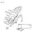
- Figure 14 shows the overall configuration of the portable pulse counter in this example.
- portable pulse counter 1001 of this example primarily comprises device main body 1010 possessing a wristwatch structure, cable 1020 connected to this device main body 1010, and pulse sensor unit 1030 installed on a first tip of this cable 1020.
- a second tip of cable 1020 is provided with connector piece 1080 which is detachably attached to connector area 1070 provided on the 6 o'clock side of device main body 1010.
- Wristband 1012 which is wrapped around the wrist from the 12 o'clock direction of the wristwatch and fastened in the 6 o'clock direction, is installed in device main body 1010; and this wristband 12 allows device main body 1010 to be easily put on or taken off from the wrist.
- Pulse wave sensor unit 1030 is attached to the area between the base of the index finger and a finger joint and is shielded from light by sensor-fastening strap 1040. Attaching pulse wave sensor unit 1030 to the base of a finger in this way keeps cable 1020 short and prevents it from getting in the way during running. Furthermore, taking into consideration the temperature distribution between the palm and finger tip in cold weather, the temperature at the finger tip falls substantially, while the temperature at the base of the finger falls relatively little. Therefore, attaching pulse wave sensor unit 1030 at the base of the finger enables the pulse count (status value) to be accurately measured even during a run outside on a cold day.
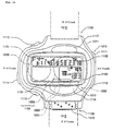
- Figure 15 is a top view showing the main body of the pulse counter of this example, with the wristband and cable removed;
- Figure 16 is a side view of this pulse counter, obtained from the 3 o'clock direction.
- device main body 1010 is provided with plastic watch case 1011 (body case), and the top side of this watch case 11 is provided with liquid crystal display device 1013 with an EL backlight for displaying running time, pitch during walking, and pulse wave information such as pulse count, in addition to current time and date.
- Liquid crystal display device 1013 is provided with first segment display area 1131 positioned on the upper left side of the display surface, second segment display area 1132 positioned on the upper right side of the display surface, third segment display area 1133 positioned on the lower right side of the display surface, and dot display area 1134 which can graphically display various types of information positioned on the lower left side of the display.
- Control area 1005 which performs various types of control and data processing in order to determine the change in the pulse count based on the pulse wave signal (status signal) measured by pulse wave sensor unit 1030 and to display the result on liquid crystal display device 1013, is provided inside watch case 1011.
- Control area 1005 is also provided with a timing circuit and thus can display normal time, lap time, split time, etc. on liquid crystal display device 1013.
- Button switches 1111 through 1115 which are used for external operations such as time adjustment and display mode switching, are provided on the perimeter of watch case 1011. Additionally, larger button switches 1116 and 1117 are provided on the surface of the watch case.
- Button-shaped small battery 1059 contained inside watch case 1011 is installed in portable pulse counter 1001, and cable 1020 supplies electrical power from battery 1059 to pulse wave sensor unit 1030 and at the same time inputs the detection result of pulse wave sensor unit 1030 into control area 1005 of watch case 1011.
- device main body 1010 The size of device main body 1010 must be increased as more functions are added to portable pulse counter 1001.
- device main body 1010 cannot be extended in the 6 or 12 o'clock directions of the watch because it must be worn around a wrist. Therefore, device main body 1010 uses watch case 1011 which is longer in the 3 and 9 o'clock directions than in the 6 and 12 o'clock directions.
- wristband 1012 is connected eccentrically toward the 3 o'clock side, leaving extended area 1101 in the 9 o'clock direction, viewed from wristband 12, but no such extended area in the 3 o'clock direction. Consequently, this structure, despite the use of long watch case 1011, allows free wrist movement and eliminates the possibility of the back of the hand striking watch case 1011 even when the wearer falls down.
- Flat piezoelectric element 1058 for a buzzer is positioned in the 9 o'clock direction, viewed from battery 1059, inside watch case 1011. Because battery 1059 is heavier than piezoelectric element 1058, the centre of gravity of device main body 1010 is positioned eccentrically in the 3 o'clock direction relative to its geometric centre. Because wristband 1012 is also connected eccentrically offset to the side on which the centre of gravity is located, device main body 1010 can be securely attached to the wrist. Furthermore, the positioning of battery 1059 and piezoelectric element 1058 in the planar direction allows device main body 1010 to be thin; battery cover 1118 installed on the back side as shown in Figure 16 allows the user to easily replace battery 1059.
- connecting area 1105 for holding stopping pin 1121 installed on the end of wristband 1012 is formed in the 12 o'clock direction of watch case 1011.
- Receiving area 1106 is provided in the 6 o'clock direction of watch case 1011, and said receiving area 1106 is provided with fastener 1122 through which wrist band 1012 is folded back and which holds in place the middle point of wristband 1012 wound around the wrist, in the long direction of the band.
- the area from bottom surface 1119 to receiving area 1106 is formed as an integral part of watch case 1011 and forms rotation stop area 1108 which is positioned at approximately 115° from bottom surface 1119. That is, when wristband 1012 is used to attach device main body 1010 to top area L1 (side of the back of the hand) of left wrist or arm L, bottom surface 1119 of watch case 1011 tightly contacts top area L1 of wrist L while rotation stop area 1108 contacts side area L2 where radius R is located. In this state, bottom surface 1119 of device main body 1010 more or less straddles radius R and ulna U, while rotation stop area 1108 and the area between bent area 1109 of bottom surface 1119 and rotation stop area 1108 contact radius R.
- rotation stop area 1108 and bottom surface 1119 form an anatomically ideal angle of approximately 115° as explained above, device main body 1010 will not turn around arm L even if an attempt is made to turn it in the direction of arrows A or B. Furthermore, because the rotation of device main body 1010 is restricted only in two locations on the side of the arm by bottom surface 1119 and rotation stop area 1108, bottom surface 1119 and rotation stop area 1108 securely contact the arm even if it is thin, and provide a secure rotation stopping effect and comfortable fit even if the arm is thick.
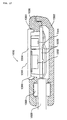
- Figure 17 shows a cross-section of the pulse sensor unit of this working example.
- component housing space 1300 is formed between the casing of pulse wave sensor unit 1030 and bottom lid 1302 on the bottom side of sensor frame 1036.
- Circuit board 1035 is positioned inside component housing space 1300.
- LED 1031, phototransistor 1032, and other electronic components are mounted on circuit board 1035.
- the first end of cable 1020 is fastened to pulse wave sensor unit 1030 by bushing 1393, and various wires of cable 1020 are soldered to various patterns on circuit board 1035.
- Pulse wave sensor unit 1030 is attached to the finger such that cable 1020 is extended from the base of the finger toward device main body 1010.
- LED 1031 and phototransistor 1032 are arranged along the length of the finger, with LED 1031 positioned on the finger tip side and phototransistor 1032 positioned at the base of the finger. This configuration provides the effect of making it difficult for the ambient light to reach phototransistor 1032.
- a light transmission window is formed by translucent plate 1034 which is made of a glass plate on the upper area of sensor frame 1036, and the light-emitting surface and light-receiving surface of LED 1031 and phototransistor 1032, respectively, are oriented toward said translucent plate 1034. Because of such a configuration, when a finger surface is pressed onto external surface 1341 of translucent plate 1034, LED 1031 emits light toward the finger surface and phototransistor 1032 can receive part of the light emitted by LED 1031 that is reflected by the finger. Note that external surface 1341 of translucent plate 1034 protrudes farther than surrounding area 1361 in order to improve its contact with the finger surface.
- an InGaN (indium-gallium-nitrogen) blue LED is used as LED 1031, and its emission spectrum possesses a peak at 450 nm and its emission wavelength ranges from 350 to 600 nm.
- a GaAsP (gallium-arsenic-phosphorus) phototransistor is used as phototransistor 1032, and the light-receiving wavelength of the element itself ranges from 300 to 600 nm, with some sensitive areas also at or below 300 nm.
- pulse wave sensor unit 1030 When pulse wave sensor unit 1030 thus configured is attached to the base of the finger by sensor-fastening strap 1040 and light is emitted from LED 1031 toward the finger, the light reaches blood vessels, and part of the light is absorbed by haemoglobin in the blood and part of it is reflected.
- the light reflected by the finger (blood) is received by phototransistor 1032, and the change in the amount of received light corresponds to the change in the blood volume (pulse wave in the blood). That is, because the reflected light becomes weak when the blood volume is high and becomes strong when the blood volume is low, data such as pulse count can be measured by optically detecting the intensity of the reflected light as a pulse wave signal.
- This working example uses LED 1031 with an emission wavelength range of between 350 and 600 nm and phototransistor 1032 with a light-receiving wavelength range of between 300 and 600 nm, and vital information is displayed based on the results taken in the overlapping wavelengths of between approximately 350 and approximately 600 nm, i.e., all wavelengths used are shorter than approximately 700 nm.
- pulse wave sensor unit 1030 is used, even if the ambient light strikes the exposed part of the finger, lights with wavelengths of 700 nm or shorter contained in the ambient light do not use the finger as a light guide to reach phototransistor 1032 (light-receiving area). The reason for this is as follows.
- the S/N ratio of the pulse wave signal based on blood volume change is high.
- the reason for this is as follows.
- the absorption coefficient of haemoglobin in the blood for lights with wavelengths of between 300 and 700 nm is several times to approximately one hundred or more times larger than the absorption coefficient for a light with wavelength of 800 nm which has been conventionally used as the detection light.
- lights with wavelengths of between 300 and 700 nm change sensitively to blood volume changes, producing higher pulse wave detection rate (S/N ratio) based on blood volume change.
- the control area 1005 is provided with pulse wave data processing area 1050 which determines the pulse count based on the input result from pulse wave sensor unit 1030, and this pulse wave data processing area 1050 outputs a pulse count calculation result, enabling this value to be displayed in liquid crystal display device 1013.
- pulse wave data processing area 1050 comprises a microcomputer that runs based on stored programs, and the functions of this microcomputer are also shown as a block diagram in Figure 18.
- pulse wave data processing area 1050 the analog signal that is input from pulse wave sensor unit 1030 is amplified by amplification circuit 1551 and is then output to analogue to digital (AD) converter 1553.
- Pulse wave data storage area 1554 is RAM that stores the pulse wave data that has been converted into a digital signal by AD converter 1553.
- Frequency analysis area 1052 is provided behind pulse wave data storage area 1554, and performs fast Fourier transformation (FFT processing) for analysing the frequency of the pulse wave data fetched from said pulse wave data storage area 1554, and this frequency analysis area 1052 inputs the frequency analysis result into pulse wave component extraction area 1053.
- Pulse wave component extraction area 1053 extracts the pulse wave component from the output signal of frequency analysis area 1052 and outputs it to pulse count calculation area 1054, and pulse count calculation area 1054 calculates the pulse count based on the frequency component of the pulse wave that was input.
- pulse wave data processing area 1050 thus configured, FFT computing units 23, 102, and 602 explained by referencing Figures 1, 5, 6, 10, and 11 can be used as frequency analysis area 1052. Since the operation of frequency analysis area 1052 (FFT computing units 23, 102, and 602) was explained earlier, its details will be omitted here.
- FFT processing is performed on the pulse wave data fetched from pulse wave data storage area 1554, a spectrum can be obtained in which individual line spectrums discretely appear with intervals corresponding to the resolutions used during frequency analysis, as schematically shown in Figure 19. Therefore, when pulse wave component extraction area 1053 identifies a target spectrum among a group of line spectrums, pulse count calculation area 1054 calculates the pulse count, and pitch, etc. based on the frequency of the target spectrum. For example, if the target spectrum appears at the position of 2 Hz, the result indicating a pulse count of 120/minute is obtained.
- the FFT computing unit based on the invention When determining the pulse count through FFT processing in this way, use of the FFT computing unit based on the invention enables FFT processing to be performed at a high level of computational precision without overflow monitoring, making a small FFT computing unit sufficient. Therefore, the FFT computing unit related to the invention is suitable for installation in portable instruments.
- pulse wave sensor unit 1030 As the comparison between pulse wave data processing area 1050 shown in Figure 18 and the FFT computation device shown in Figure 19 indicates, pulse wave sensor unit 1030, amplification circuit 1551, AD converter 1553, pulse wave data storage area 1554, and frequency analysis area 1052 shown in Figure 19 correspond to sensor 620, amplification circuit 621, AD converter 622, first RAM 625, and FFT computing unit 602 shown in Figure 9, respectively. Therefore, if level determination circuit 624 explained with reference to Figure 9 is added to pulse wave data processing area 1050 shown in Figure 18, it would not be necessary to separately allocate time for the level determination to be performed for adjusting the shift. Furthermore, if gain control circuit 623 is added, the detected signal itself before digital conversion can be controlled to a size suitable to FFT computation in an analog format.
- the invention according to Claim 1 is provided with data shift means that standardise data to a certain bit width before the sum or difference of two pieces of integer data is computed and with data conversion means that standardise bit width to a certain bit width by truncating part of output data for each output of computation means, and thus eliminates the need for overflow monitoring. Therefore, FFT computation can be carried out at a high level of computational precision without any complicated control means, making it possible to implement a small FFT computing unit.
- the invention according to Claim 2 uses sine and cosine wave data that has been turned into an integer by multiplying the sine and cosine wave data of a real number by 2 n-1 , truncating positive numbers, and rounding up negative numbers, and that has been converted into a number such that its bits excluding the sign can be expressed within n - 1 bits, and thus truncation errors during the FFT computation process can be made smaller than when sine and cosine wave data expressed in another format is used. Therefore, a high level of computational precision can be achieved since the truncation caused by rounding-up during FFT computation can be prevented.
- the highest bit of the output data excluding the sign bit, is truncated when converting either the output of the multiplication means or the output of the addition/subtraction means that computes the sum or difference of the multiplication means, and thus the data shift is adjusted by performing truncation/rounding-up during the computation process that is least likely to produce degradation in computational precision, among the computation processes of the imaginary part in which more computations take place than in the real part. Therefore, a high level of computational precision can be achieved by making the shift the same as that used when obtaining the computation result for the real part.
- the invention according to Claim 4 is provided with a shift adjustment means for adjusting the data shift in accordance with the size of the FFT computation target data, and thus a larger number of effective digits can be obtained during computation, producing a high level of computational precision.
- the size of the transferred data is determined by the level determination means, and the shift is adjusted based on the determined level, and thus it is not necessary to separately allocate time for the level determination to be performed for adjusting the shift.
- the invention according to Claim 6 is provided with the gain control means which, after the specified number of pieces of data is stored in the first storage means which sequentially stores the digitally converted output signal from the amplification means, and simultaneously with sending of the FFT target data to the second storage means, determines the size of the transferred data, and which, based on the determined level, changes the amplification factor of the amplification means for amplifying the signal detected by the signal detection means to an appropriate value, and thus the detected signal itself before digital conversion can be controlled to a size suitable to FFT computation in an analog format. Therefore, computational precision in subsequent FFT computation results can be improved when FFT computations are continuously made.
Landscapes
- Physics & Mathematics (AREA)
- Mathematical Physics (AREA)
- Engineering & Computer Science (AREA)
- General Physics & Mathematics (AREA)
- Computational Mathematics (AREA)
- Mathematical Analysis (AREA)
- Mathematical Optimization (AREA)
- Pure & Applied Mathematics (AREA)
- Data Mining & Analysis (AREA)
- Theoretical Computer Science (AREA)
- Discrete Mathematics (AREA)
- Algebra (AREA)
- Databases & Information Systems (AREA)
- Software Systems (AREA)
- General Engineering & Computer Science (AREA)
- Complex Calculations (AREA)
Claims (7)
- Berechnungseinheit für schnelle Fourier-Transformation, mit einem ersten (5) und einem zweiten (6) Additions/Subtraktions-Mittel zum Berechnen und Ausgeben einer Summe oder einer Differenz eines Paares von Ganzzahlen-Daten, einem ersten (8) und einem zweiten (9) Multiplikationsmittel, das die Ausgänge des ersten und des zweiten Additions/Subtraktions-Mittels mit einem Sinus- bzw. Kosinuswellen-Datensignal (7) multipliziert, und einem dritten Additions/Subtraktions-Mittel (10), das die Summe und die Differenz der Ausgänge von beiden Multiplikationsmitteln berechnet, dadurch gekennzeichnet, daß die Berechnungseinheit für die schnelle Fourier-Transformation umfaßt:Datenschiebemittel (1,2,3,4), die die Eingangsdaten für die Berechnungseinheit auf eine vorgegebene Bitbreite normieren durch Verschieben der Eingangsdaten um ein Datenverschiebungsmaß, das ermittelt wird anhand der Größe der Eingangsdaten, um somit die Daten des Paares von Ganzzahlen-Daten als Eingabe in das erste und das zweite Additions/Subtraktions-Mittel zu bilden;Datenumwandlungsmittel (11, 12, 13, 14,15), die die vom ersten (5), vom zweiten (6) und vom dritten (10) Additions/Subtraktions-Mittel und vom ersten (8) und vom zweiten (9) Multiplikationsmittel gelieferten Daten auf die vorgegebene Bitbreite normieren durch Abrunden des höchstwertigen Teils dieser Ausgangsdaten, ausschließlich des Vorzeichenbits.
- Berechnungseinheit für schnelle Fourier-Transformation nach Anspruch 1, die ferner dadurch gekennzeichnet ist, daß dann, wenn die Eingangsbitbreite jeweils des ersten, des zweiten und des dritten Additions/Subtraktions-Mittels und des ersten und des zweiten Multiplikationsmittels gleich n Bits ist, die Sinus- und Kosinuswellen-Daten in eine Ganzzahl umgewandelt werden durch Multiplizieren der Sinus- und Kosinuswellen-Daten einer Realzahl mit 2n-1, Abrunden der positiven Zahlen und Aufrunden der negativen Zahlen, deren Bits ausschließlich des Vorzeichens innerhalb von n-1 Bits ausgedrückt werden können.
- Berechnungseinheit für schnelle Fourier-Transformation nach Anspruch 1 oder Anspruch 2, ferner dadurch gekennzeichnet, daß die Datenumwandlungsmittel das höchste Bit der Ausgangsdaten, ausschließlich des Vorzeichenbits, abrunden, wenn die Ausgangsdaten des ersten und/oder des zweiten Multiplikationsmittels und des dritten Additions/Subtraktions-Mittels (10) umgewandelt werden.
- Berechnungseinheit für schnelle Fourier-Transformation nach irgendeinem der vorangehenden Ansprüche, ferner dadurch gekennzeichnet, daß die Datenschiebemittel mit einem Verschiebungseinstellmittel versehen sind zum Einstellen der Datenverschiebung entsprechend der Größe der Zieldaten der schnellen Fourier-Transformationsberechnung.
- Berechnungsvorrichtung für schnelle Fourier-Transformation, die mit einer Berechnungseinheit für schnelle Fourier-Transformation (23) gemäß Anspruch 4 ausgestattet ist, und die umfaßt: ein erstes Speichermittel (20) zum sequentiellen Speichern der Daten, die in einer Zeitreihe eingegeben werden, ein zweites Speichermittel (21) zum Speichern sowohl der Zieldaten der schnellen Fourier-Transformationsberechnung als auch der berechneten Daten, ein Niveauermittlungsmittel (24) zum Ermitteln der Größe der im zweiten Speichermittel (21) gespeicherten Daten, und ein drittes Speichermittel (22) zum Speichern der Sinuswellen- und Kosinuswellen-Daten für die Berechnung; und die ferner dadurch gekennzeichnet ist, daß die Fourier-Transformationsberechnung mittels der Berechnungseinheit für schnelle Fourier-Transformation (23) durchgeführt wird unter Verwendung der Daten sowohl vom zweiten Speichermittel (21) als auch vom dritten Speichermittel (22); und
daß nach der Speicherung der spezifizierten Anzahl von Datenelementen im ersten Speichermittel (20) gleichzeitig mit dem Senden der Zieldaten der schnellen Fourier-Transformationsberechnung zum zweiten Speichermittel (21) die Größe der übertragenen Daten durch das Niveau-Ermittlungsmittel (24) ermittelt wird, wobei das Verschiebungseinstellmittel die Datenverschiebung auf der Grundlage des ermittelten Niveaus einstellt. - Berechnungsvorrichtung für schnelle Fourier-Transformation, die mit einer Berechnungseinheit für schnelle Fourier-Transformation (23) gemäß irgendeinem der Ansprüche 1 bis 4 ausgestattet ist, und die umfaßt: ein Verstärkungsmittel (31) zum Verstärken des vom Signalerfassungsmittel (30) erfaßten Signals, ein Verstärkungsfaktorsteuermittel (33) zum Ändern des Verstärkungsfaktors dieses Verstärkungsmittels (31), ein erstes Speichermittel (20) zum sequentielles Speichern der Ausgangssignale des Verstärkungsmittels (31), die vom Signalumwandlungsmittel (32) in Digitalsignale umgewandelt worden sind, ein zweites Speichermittel (21) zum Speichern sowohl der Zieldaten der schnellen Fourier-Transformationsberechnung als auch der berechneten Daten, ein Niveauermittlungsmittel (24) zum Ermitteln der Größe der in diesem zweiten Speichermittel (21) gespeicherten Daten, und ein drittes Speichermittel (22) zum Speichern der Sinuswellen- und Kosinuswellen-Daten für die Berechnung; und die ferner dadurch gekennzeichnet ist, daß die Fourier-Transformationsberechnung mittels der Berechnungseinheit für schnelle Fourier-Transformation (23) durchgeführt wird unter Verwendung der Daten sowohl vom zweiten Speichermittel (21) als auch vom dritten Speichermittel (22); und
daß nach der Speicherung der spezifizierten Anzahl von Datenelementen im ersten Speichermittel (20) gleichzeitig mit dem Senden der Zieldaten der schnellen Fourier-Transformationsberechnung zum zweiten Speichermittel (21) die Größe der übertragenen Daten durch das Niveau-Ermittlungsmittel (24) ermittelt wird, wobei das Verstärkungsfaktorsteuermittel (33) auf der Grundlage des Ermittlungsergebnisses den Verstärkungsfaktor des Verstärkungsmittels (31) ändert. - Impulszähler, dadurch gekennzeichnet, daß er die Berechnungseinheit für schnelle Fourier-Transformation (23) gemäß irgendeinem der Ansprüche 1 bis 4 verwendet, um die Frequenz eines Impulswellensignals zu analysieren, das mittels eines Impulswellensensors gemessen wird, und um den Impulszählerstand auf der Grundlage des Frequenzanalyseergebnisses zu ermitteln.
Applications Claiming Priority (6)
| Application Number | Priority Date | Filing Date | Title |
|---|---|---|---|
| JP21929395 | 1995-08-28 | ||
| JP219293/95 | 1995-08-28 | ||
| JP21929395 | 1995-08-28 | ||
| JP154671/96 | 1996-06-14 | ||
| JP15467196A JP3665423B2 (ja) | 1995-08-28 | 1996-06-14 | 高速フーリエ変換演算器及び高速フーリエ変換演算装置 |
| JP15467196 | 1996-06-14 |
Publications (2)
| Publication Number | Publication Date |
|---|---|
| EP0762296A1 EP0762296A1 (de) | 1997-03-12 |
| EP0762296B1 true EP0762296B1 (de) | 2002-05-22 |
Family
ID=26482895
Family Applications (1)
| Application Number | Title | Priority Date | Filing Date |
|---|---|---|---|
| EP96306206A Expired - Lifetime EP0762296B1 (de) | 1995-08-28 | 1996-08-27 | Einheit und Gerät zur schnellen Fourier-Transformationsberechnung |
Country Status (4)
| Country | Link |
|---|---|
| US (1) | US5854758A (de) |
| EP (1) | EP0762296B1 (de) |
| JP (1) | JP3665423B2 (de) |
| DE (1) | DE69621298T2 (de) |
Families Citing this family (14)
| Publication number | Priority date | Publication date | Assignee | Title |
|---|---|---|---|---|
| DE19706160A1 (de) | 1997-02-17 | 1998-08-20 | Heidelberger Druckmasch Ag | Verfahren zur Abtastung von gerasterten Bildvorlagen |
| US7890566B1 (en) * | 2000-02-18 | 2011-02-15 | Texas Instruments Incorporated | Microprocessor with rounding dot product instruction |
| US6996597B2 (en) * | 2001-06-15 | 2006-02-07 | Centillium Communications, Inc. | Increasing precision in multi-stage processing of digital signals |
| US7187935B1 (en) | 2001-10-16 | 2007-03-06 | International Business Machines Corporation | Method and software for low bandwidth presence via aggregation and profiling |
| US20030212721A1 (en) * | 2002-05-07 | 2003-11-13 | Infineon Technologies Aktiengesellschaft | Architecture for performing fast fourier transforms and inverse fast fourier transforms |
| US20030212722A1 (en) * | 2002-05-07 | 2003-11-13 | Infineon Technologies Aktiengesellschaft. | Architecture for performing fast fourier-type transforms |
| CN101057474B (zh) * | 2004-11-16 | 2010-12-01 | 三星电子株式会社 | 在正交频分多址无线通信系统中处理数字信号的装置和方法 |
| US7861060B1 (en) | 2005-12-15 | 2010-12-28 | Nvidia Corporation | Parallel data processing systems and methods using cooperative thread arrays and thread identifier values to determine processing behavior |
| US20070242530A1 (en) * | 2006-04-13 | 2007-10-18 | Hsiang-I Huang | Memory controller for supporting double data rate memory and related method |
| US7640284B1 (en) | 2006-06-15 | 2009-12-29 | Nvidia Corporation | Bit reversal methods for a parallel processor |
| US7836116B1 (en) * | 2006-06-15 | 2010-11-16 | Nvidia Corporation | Fast fourier transforms and related transforms using cooperative thread arrays |
| US8601044B2 (en) * | 2010-03-02 | 2013-12-03 | Altera Corporation | Discrete Fourier Transform in an integrated circuit device |
| JP2012151561A (ja) * | 2011-01-17 | 2012-08-09 | Seiko Epson Corp | A/d変換回路、集積回路装置及び電子機器 |
| CN106470172B (zh) * | 2015-08-14 | 2020-01-24 | 扬智科技股份有限公司 | 快速傅立叶变换增益调整电路与方法 |
Family Cites Families (10)
| Publication number | Priority date | Publication date | Assignee | Title |
|---|---|---|---|---|
| US3778606A (en) * | 1972-02-23 | 1973-12-11 | Sanders Associates Inc | Continuously updating fourier coefficients every sampling interval |
| US3927312A (en) * | 1974-10-31 | 1975-12-16 | Us Army | Vector rotator |
| US4393457A (en) * | 1981-03-26 | 1983-07-12 | Advanced Micro Devices, Inc. | Method and apparatus for sequencing addresses of a fast Fourier transform array |
| US4612626A (en) * | 1983-12-27 | 1986-09-16 | Motorola Inc. | Method of performing real input fast fourier transforms simultaneously on two data streams |
| JPS61170442A (ja) * | 1985-01-23 | 1986-08-01 | 松下電器産業株式会社 | 超音波ドツプラ血流装置 |
| JPH0644225B2 (ja) * | 1986-03-27 | 1994-06-08 | 日本電気株式会社 | 浮動小数点丸め正規化回路 |
| FR2599872B1 (fr) * | 1986-06-06 | 1988-07-29 | Thomson Csf | Dispositifs de calcul de transformees cosinus mono-dimensionnelles, et dispositif de codage et dispositif de decodage d'images comportant de tels dispositifs de calcul |
| US5091875A (en) * | 1990-03-23 | 1992-02-25 | Texas Instruments Incorporated | Fast fourier transform (FFT) addressing apparatus and method |
| US5095456A (en) * | 1990-03-23 | 1992-03-10 | Texas Instruments Incorporated | Method for densely packing a complex multiplier |
| FR2709007B1 (fr) * | 1993-08-11 | 1995-09-29 | Joanblanq Christophe | Dispositif électronique de calcul d'une transformée de Fourier et procédé pour minimiser la taille des chemins de données internes d'un tel dispositif. |
-
1996
- 1996-06-14 JP JP15467196A patent/JP3665423B2/ja not_active Expired - Lifetime
- 1996-08-06 US US08/692,991 patent/US5854758A/en not_active Expired - Lifetime
- 1996-08-27 EP EP96306206A patent/EP0762296B1/de not_active Expired - Lifetime
- 1996-08-27 DE DE69621298T patent/DE69621298T2/de not_active Expired - Lifetime
Also Published As
| Publication number | Publication date |
|---|---|
| JPH09128374A (ja) | 1997-05-16 |
| JP3665423B2 (ja) | 2005-06-29 |
| DE69621298D1 (de) | 2002-06-27 |
| DE69621298T2 (de) | 2002-10-17 |
| EP0762296A1 (de) | 1997-03-12 |
| US5854758A (en) | 1998-12-29 |
Similar Documents
| Publication | Publication Date | Title |
|---|---|---|
| EP0762296B1 (de) | Einheit und Gerät zur schnellen Fourier-Transformationsberechnung | |
| EP0729726B1 (de) | Pulsschlagmesser | |
| US5906582A (en) | Organism information measuring method and arm wear type pulse-wave measuring method | |
| US5759156A (en) | Period and frequency measurement device with correction device and method thereof | |
| EP0667515B1 (de) | Druckfühler, vorrichtung zur messung von druckschwingungen ausgerüstet mit einemderartigen fühler und gerät zur feststellung von pulswellen | |
| US6155983A (en) | Pulse wave detecting device and pulse measurer | |
| HK1010061B (en) | Pressure sensor, pressure vibration detection apparatus using the sensor, and pulse wave detection apparatus | |
| WO1998041142A1 (en) | Pulsometer and pulsation indication method | |
| EP0803733B1 (de) | Messinstrument, tragbares elektronisches gerät und messverfahren | |
| HK1014775A (en) | A fast fourier transformation computing unit and fast fourier transformation computation device | |
| CN218128538U (zh) | 一种电子设备 | |
| JPH09113309A (ja) | 計測装置 | |
| JP2005137677A (ja) | 計測装置、計測装置の制御方法、制御プログラムおよび記録媒体 | |
| HK1014475A (en) | Pulse rate meter | |
| US12490939B2 (en) | Optical sensor in a button of an electronic device | |
| JPH08266493A (ja) | 腕装着型脈波計測装置 | |
| CN216876377U (zh) | 便携式智能设备 | |
| CN212181270U (zh) | 智能手表 | |
| JP3554085B2 (ja) | 脈波情報計測装置 | |
| JP2000083914A (ja) | 生体情報計測装置および脈波計測装置 | |
| JPH0910183A (ja) | 携帯装置および腕装着型脈波計測装置 | |
| JPH09135818A (ja) | 携帯用電子機器 | |
| KR20230081828A (ko) | 운동기구에 부착되어 신호검출, 분석, 전송을 행하는 올인원형 운동 및 건강정보 분석 장치 | |
| JPS54121774A (en) | Electronic watch with calculator | |
| MA | Block sum register and burst arithmetic[M. S. Thesis] |
Legal Events
| Date | Code | Title | Description |
|---|---|---|---|
| PUAI | Public reference made under article 153(3) epc to a published international application that has entered the european phase |
Free format text: ORIGINAL CODE: 0009012 |
|
| AK | Designated contracting states |
Kind code of ref document: A1 Designated state(s): DE FI FR GB |
|
| 17P | Request for examination filed |
Effective date: 19970818 |
|
| GRAG | Despatch of communication of intention to grant |
Free format text: ORIGINAL CODE: EPIDOS AGRA |
|
| 17Q | First examination report despatched |
Effective date: 20010903 |
|
| GRAG | Despatch of communication of intention to grant |
Free format text: ORIGINAL CODE: EPIDOS AGRA |
|
| GRAH | Despatch of communication of intention to grant a patent |
Free format text: ORIGINAL CODE: EPIDOS IGRA |
|
| GRAH | Despatch of communication of intention to grant a patent |
Free format text: ORIGINAL CODE: EPIDOS IGRA |
|
| GRAA | (expected) grant |
Free format text: ORIGINAL CODE: 0009210 |
|
| REG | Reference to a national code |
Ref country code: GB Ref legal event code: FG4D |
|
| REF | Corresponds to: |
Ref document number: 69621298 Country of ref document: DE Date of ref document: 20020627 |
|
| ET | Fr: translation filed | ||
| PLBE | No opposition filed within time limit |
Free format text: ORIGINAL CODE: 0009261 |
|
| STAA | Information on the status of an ep patent application or granted ep patent |
Free format text: STATUS: NO OPPOSITION FILED WITHIN TIME LIMIT |
|
| 26N | No opposition filed |
Effective date: 20030225 |
|
| REG | Reference to a national code |
Ref country code: HK Ref legal event code: WD Ref document number: 1014775 Country of ref document: HK |
|
| REG | Reference to a national code |
Ref country code: FR Ref legal event code: PLFP Year of fee payment: 20 |
|
| PGFP | Annual fee paid to national office [announced via postgrant information from national office to epo] |
Ref country code: GB Payment date: 20150826 Year of fee payment: 20 Ref country code: FI Payment date: 20150810 Year of fee payment: 20 Ref country code: DE Payment date: 20150818 Year of fee payment: 20 |
|
| PGFP | Annual fee paid to national office [announced via postgrant information from national office to epo] |
Ref country code: FR Payment date: 20150629 Year of fee payment: 20 |
|
| REG | Reference to a national code |
Ref country code: DE Ref legal event code: R071 Ref document number: 69621298 Country of ref document: DE |
|
| REG | Reference to a national code |
Ref country code: GB Ref legal event code: PE20 Expiry date: 20160826 |
|
| PG25 | Lapsed in a contracting state [announced via postgrant information from national office to epo] |
Ref country code: GB Free format text: LAPSE BECAUSE OF EXPIRATION OF PROTECTION Effective date: 20160826 |