EP0772835B1 - Arrangement at an image processor - Google Patents
Arrangement at an image processor Download PDFInfo
- Publication number
- EP0772835B1 EP0772835B1 EP95926571A EP95926571A EP0772835B1 EP 0772835 B1 EP0772835 B1 EP 0772835B1 EP 95926571 A EP95926571 A EP 95926571A EP 95926571 A EP95926571 A EP 95926571A EP 0772835 B1 EP0772835 B1 EP 0772835B1
- Authority
- EP
- European Patent Office
- Prior art keywords
- unit
- unit block
- incrementing
- processor
- units
- Prior art date
- Legal status (The legal status is an assumption and is not a legal conclusion. Google has not performed a legal analysis and makes no representation as to the accuracy of the status listed.)
- Expired - Lifetime
Links
Images


Classifications
-
- G—PHYSICS
- G06—COMPUTING OR CALCULATING; COUNTING
- G06T—IMAGE DATA PROCESSING OR GENERATION, IN GENERAL
- G06T1/00—General purpose image data processing
- G06T1/20—Processor architectures; Processor configuration, e.g. pipelining
-
- G—PHYSICS
- G06—COMPUTING OR CALCULATING; COUNTING
- G06F—ELECTRIC DIGITAL DATA PROCESSING
- G06F15/00—Digital computers in general; Data processing equipment in general
- G06F15/76—Architectures of general purpose stored program computers
- G06F15/80—Architectures of general purpose stored program computers comprising an array of processing units with common control, e.g. single instruction multiple data processors
- G06F15/8007—Architectures of general purpose stored program computers comprising an array of processing units with common control, e.g. single instruction multiple data processors single instruction multiple data [SIMD] multiprocessors
- G06F15/8015—One dimensional arrays, e.g. rings, linear arrays, buses
Definitions
- the present invention relates to a device in a parallel processor containing a number of processor elements of the same type which are integrated on one and the same semiconductor chip, and which are of the kind that allows parallel image or signal processing of the information stored in the processor element, whereby the said device contains a unit block for each processor element.
- a way of achieving a high processing speed is to use units with an integrated unit solution comprising both a camera in the form of a photodiode matrix and an image processor.
- an image processor which contains a device able to indicate the image dots belonging to a connected object, and produces a binary signal corresponding to the object when the relevant image dot, on the one hand, meets a condition specific to the object, and, on the other hand, is indicated as entering the object, or when the closest adjacent image dots are distinguished.
- a drawback with the known technique is that the known processors cannot perform so-called arithmetic global operations with the same efficiency, for example determine the centre of median for every object in a read-in vector.
- the known device there takes place with this type of operation a serial outputting of image data which, in per se time terms, reduces the advantages of the fast image processors.
- each unit block comprises at least two incrementing units which are designed to add a signal supplied to the unit block, and a signal which originates from an incrementing unit corresponding to the respective unit in the closest preceding unit block in every direction of the processor element matrix, and in that every unit block further contains at least one logical unit which is designed to perform logical operations of Boolean type on the signals received from the incrementing units of the unit block.
- said signal supplied to the unit block corresponds to an image or radar signal coming from a processor element.
- the number of incrementing units in every unit block is two, and the device is preferably designed to be used in line image processing and signal processing.
- said incrementing units each contain a plurality of half adders, an AND-gate is connected to one input on the respective half adders, and one input of the AND-gate is connected to the output of the corresponding half adder in the preceding incrementing unit.
- every incrementing unit contains precisely one half adder over the logarithm of base two of the number of processor elements arranged in line.
- said logical unit is designed to compare the values of the incrementing units in every unit block.
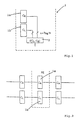
- Figure 1 shows a unit block of the invention.
- Figure 2 shows the incrementing units in differing unit blocks, and
- Figure 3 shows a preferred implementation of an incrementing unit.
- Figures 4-7 show examples of different arithmetic global operations that can be carried out with a device of the invention.
- the device of the invention is preferably designed for line image processing, and the description which follows is based on this preferred form of embodiment.
- Each processor element (PE) is connected with a unit block 3 corresponding to the element, which contains two incrementing units 1a, 1b with a preferred embodiment according to Figure 1.
- Said incrementing unit makes it possible to increase the value originating from the adjacent unit block.
- the function that is carried out in every unit block may be described by the equation.
- X i P i ⁇ X i-1 +D i
- each unit block contains two incrementing units; one for each direction in the matrix of the processor element, as may be seen in Figure 3. Apart from the spread direction of the units, these two incrementing units are identical.
- Figure 1 shows a block diagram of a complete unit block of the invention.
- the two incrementing units 1a, 1b are connected with a logical unit 2 which can perform Boolean logic operations on the signals received from the incrementing units of the unit block.
- the logical unit is furthermore connected with an accumulator register in the image processor.
- a logical operation of the type is carried out in said logical unit.
- the centre point in the area between two objects may be determined in a manner which resembles the one given above, with the exception that the image vector is inverted while the ramp formation takes place in the incrementing units.
- the incrementing units are to perform a summation function at which the value of the image dot corresponding to a unit block is added to the accumulated value for all preceding image dots, as shown in Figure 5.
- a global shift implies that the whole object is shifted to the right side of the vector.
- the incrementing units in the respective unit block must perform various types of summation operations, as may be seen in Figure 6.
- the value of an image dot corresponding to a unit block is added to the accumulated value for the preceding image points in the same manner as for the determination of the image vector mean.
- a ramp formation takes place in that P i and D 1 must both assume the value 1.
- the comparing logical unit there is formed a vector having a number of consecutive ones and the result is determined in the same way as before in that the right side for the consecutive ones is established.
Landscapes
- Engineering & Computer Science (AREA)
- Theoretical Computer Science (AREA)
- Computer Hardware Design (AREA)
- Physics & Mathematics (AREA)
- General Physics & Mathematics (AREA)
- Computing Systems (AREA)
- General Engineering & Computer Science (AREA)
- Image Processing (AREA)
- Logic Circuits (AREA)
- Pharmaceuticals Containing Other Organic And Inorganic Compounds (AREA)
- Ultra Sonic Daignosis Equipment (AREA)
- Processing Or Creating Images (AREA)
- Measuring And Recording Apparatus For Diagnosis (AREA)
- Manufacture Or Reproduction Of Printing Formes (AREA)
- Advance Control (AREA)
- Multi Processors (AREA)
Applications Claiming Priority (3)
| Application Number | Priority Date | Filing Date | Title |
|---|---|---|---|
| SE9402551 | 1994-07-22 | ||
| SE9402551A SE9402551L (sv) | 1994-07-22 | 1994-07-22 | Anordning vid en bildbehandlingsprocessor |
| PCT/SE1995/000868 WO1996003700A1 (en) | 1994-07-22 | 1995-07-18 | Arrangement at an image processor |
Publications (2)
| Publication Number | Publication Date |
|---|---|
| EP0772835A1 EP0772835A1 (en) | 1997-05-14 |
| EP0772835B1 true EP0772835B1 (en) | 2000-03-01 |
Family
ID=20394787
Family Applications (1)
| Application Number | Title | Priority Date | Filing Date |
|---|---|---|---|
| EP95926571A Expired - Lifetime EP0772835B1 (en) | 1994-07-22 | 1995-07-18 | Arrangement at an image processor |
Country Status (11)
| Country | Link |
|---|---|
| US (1) | US5982393A (pt) |
| EP (1) | EP0772835B1 (pt) |
| JP (1) | JP2000509170A (pt) |
| CN (1) | CN1098494C (pt) |
| AT (1) | ATE190152T1 (pt) |
| AU (1) | AU685311B2 (pt) |
| BR (1) | BR9508422A (pt) |
| CA (1) | CA2195674A1 (pt) |
| DE (1) | DE69515311T2 (pt) |
| SE (1) | SE9402551L (pt) |
| WO (1) | WO1996003700A1 (pt) |
Families Citing this family (4)
| Publication number | Priority date | Publication date | Assignee | Title |
|---|---|---|---|---|
| US6825936B2 (en) | 2000-08-23 | 2004-11-30 | Lmi Technologies, Inc. | High speed camera based sensors |
| US6618155B2 (en) | 2000-08-23 | 2003-09-09 | Lmi Technologies Inc. | Method and apparatus for scanning lumber and other objects |
| NO316877B1 (no) | 2001-07-18 | 2004-06-07 | Hts Hans Torgersen & Sonn As | Festesystem for barnesete |
| US20050185102A1 (en) * | 2004-01-06 | 2005-08-25 | Fairhurst Jon A. | Single touch launch of remote applications over video |
Family Cites Families (8)
| Publication number | Priority date | Publication date | Assignee | Title |
|---|---|---|---|---|
| SE431145B (sv) * | 1983-03-15 | 1984-01-16 | Robert Forchheimer | Anordning vid en uppsettning, i matrisform anordnade fotodioder |
| GB8707493D0 (en) * | 1987-03-28 | 1987-08-05 | Stonefield Systems Plc | Cellular array processing |
| KR0184865B1 (ko) * | 1989-10-13 | 1999-05-15 | 엔. 라이스 머레트 | 데이타 프로세싱 디바이스 |
| SE466074B (sv) * | 1990-04-30 | 1991-12-09 | Gennum Corp | Digital signalbehandlingsanordning med processorelement som innefattar en enbitsbuss |
| JP2770603B2 (ja) * | 1991-03-14 | 1998-07-02 | 三菱電機株式会社 | 並列計算機 |
| JPH05189549A (ja) * | 1991-09-10 | 1993-07-30 | Kubota Corp | マルチプロセッサによる画像データ処理装置 |
| JP3098342B2 (ja) * | 1992-11-26 | 2000-10-16 | 富士通株式会社 | 並列処理装置における処理順序指定方式 |
| US5557734A (en) * | 1994-06-17 | 1996-09-17 | Applied Intelligent Systems, Inc. | Cache burst architecture for parallel processing, such as for image processing |
-
1994
- 1994-07-22 SE SE9402551A patent/SE9402551L/ not_active IP Right Cessation
-
1995
- 1995-07-18 DE DE69515311T patent/DE69515311T2/de not_active Expired - Lifetime
- 1995-07-18 EP EP95926571A patent/EP0772835B1/en not_active Expired - Lifetime
- 1995-07-18 US US08/776,070 patent/US5982393A/en not_active Expired - Lifetime
- 1995-07-18 CN CN95194195A patent/CN1098494C/zh not_active Expired - Fee Related
- 1995-07-18 AT AT95926571T patent/ATE190152T1/de not_active IP Right Cessation
- 1995-07-18 AU AU30901/95A patent/AU685311B2/en not_active Ceased
- 1995-07-18 BR BR9508422A patent/BR9508422A/pt not_active Application Discontinuation
- 1995-07-18 JP JP8505689A patent/JP2000509170A/ja active Pending
- 1995-07-18 WO PCT/SE1995/000868 patent/WO1996003700A1/en not_active Ceased
- 1995-07-18 CA CA002195674A patent/CA2195674A1/en not_active Abandoned
Also Published As
| Publication number | Publication date |
|---|---|
| WO1996003700A1 (en) | 1996-02-08 |
| SE502485C2 (sv) | 1995-10-30 |
| DE69515311T2 (de) | 2000-10-19 |
| US5982393A (en) | 1999-11-09 |
| DE69515311D1 (de) | 2000-04-06 |
| JP2000509170A (ja) | 2000-07-18 |
| BR9508422A (pt) | 1997-11-18 |
| CN1098494C (zh) | 2003-01-08 |
| EP0772835A1 (en) | 1997-05-14 |
| AU685311B2 (en) | 1998-01-15 |
| AU3090195A (en) | 1996-02-22 |
| MX9700528A (es) | 1998-05-31 |
| CN1152966A (zh) | 1997-06-25 |
| SE9402551L (sv) | 1995-10-30 |
| CA2195674A1 (en) | 1996-02-08 |
| ATE190152T1 (de) | 2000-03-15 |
| SE9402551D0 (sv) | 1994-07-22 |
Similar Documents
| Publication | Publication Date | Title |
|---|---|---|
| EP0685127B1 (en) | Calculation of a scalar product in a direct-type fir filter | |
| AU613635B2 (en) | Apparatus for detecting pattern of crest line | |
| EP0772835B1 (en) | Arrangement at an image processor | |
| KR100302093B1 (ko) | 교차형디지탈유한임펄스응답필터에서이진입력신호를탭계수와승산시키는방법및회로배열과교차형디지탈필터의설계방법 | |
| JPH07273638A (ja) | 複数広域入力機能のためのプログラム式専用fpga機能ブロックを備えたfpgaアーキテクチャ | |
| GB2265462A (en) | Three-dimensional maximum a posteriori (map) tracking | |
| EP0997828A3 (en) | Signal processing distributed arithmetic architecture | |
| Handelman | Deciding eventual positivity of polynomials | |
| US5819026A (en) | System and method for arbitrating accelerator requests | |
| US4546445A (en) | Systolic computational array | |
| EP1052568A1 (en) | Three input split-adder | |
| EP0655675B1 (en) | Shift and rounding circuit and method | |
| EP0500048B1 (en) | Orthogonal transform apparatus for video signal processing | |
| MXPA97000528A (en) | Configuration in an image processor | |
| RU2093957C1 (ru) | Устройство для сжатия данных (варианты) | |
| KR100241071B1 (ko) | 합과 합+1을 병렬로 생성하는 가산기 | |
| EP0482003B1 (en) | Audio signal processor circuit | |
| RU2093958C1 (ru) | Устройство для сжатия данных (варианты) | |
| KR100298127B1 (ko) | 덧셈기만을 사용한 비트 분리 구조의 고속 병렬 디지털 필터 | |
| JP2961246B2 (ja) | 多眼ステレオ画像処理のための複数画像を統合化する画像処理方式 | |
| RU2042191C1 (ru) | Устройство для распределения заданий в вычислительной системе | |
| US4811271A (en) | Expandable bi-phase convolving element | |
| JPH0320880A (ja) | 変換回路 | |
| SU1091189A1 (ru) | Экстрапол тор видеосигнала изображени | |
| US4933894A (en) | Circuit and method for adding binary numbers with a difference of one or less |
Legal Events
| Date | Code | Title | Description |
|---|---|---|---|
| PUAI | Public reference made under article 153(3) epc to a published international application that has entered the european phase |
Free format text: ORIGINAL CODE: 0009012 |
|
| 17P | Request for examination filed |
Effective date: 19970113 |
|
| AK | Designated contracting states |
Kind code of ref document: A1 Designated state(s): AT BE DE ES FR GB IE IT NL |
|
| GRAG | Despatch of communication of intention to grant |
Free format text: ORIGINAL CODE: EPIDOS AGRA |
|
| 17Q | First examination report despatched |
Effective date: 19990428 |
|
| GRAG | Despatch of communication of intention to grant |
Free format text: ORIGINAL CODE: EPIDOS AGRA |
|
| GRAH | Despatch of communication of intention to grant a patent |
Free format text: ORIGINAL CODE: EPIDOS IGRA |
|
| GRAH | Despatch of communication of intention to grant a patent |
Free format text: ORIGINAL CODE: EPIDOS IGRA |
|
| GRAA | (expected) grant |
Free format text: ORIGINAL CODE: 0009210 |
|
| AK | Designated contracting states |
Kind code of ref document: B1 Designated state(s): AT BE DE ES FR GB IE IT NL |
|
| PG25 | Lapsed in a contracting state [announced via postgrant information from national office to epo] |
Ref country code: NL Free format text: LAPSE BECAUSE OF FAILURE TO SUBMIT A TRANSLATION OF THE DESCRIPTION OR TO PAY THE FEE WITHIN THE PRESCRIBED TIME-LIMIT Effective date: 20000301 Ref country code: IT Free format text: LAPSE BECAUSE OF FAILURE TO SUBMIT A TRANSLATION OF THE DESCRIPTION OR TO PAY THE FEE WITHIN THE PRESCRIBED TIME-LIMIT;WARNING: LAPSES OF ITALIAN PATENTS WITH EFFECTIVE DATE BEFORE 2007 MAY HAVE OCCURRED AT ANY TIME BEFORE 2007. THE CORRECT EFFECTIVE DATE MAY BE DIFFERENT FROM THE ONE RECORDED. Effective date: 20000301 Ref country code: ES Free format text: THE PATENT HAS BEEN ANNULLED BY A DECISION OF A NATIONAL AUTHORITY Effective date: 20000301 Ref country code: BE Free format text: LAPSE BECAUSE OF FAILURE TO SUBMIT A TRANSLATION OF THE DESCRIPTION OR TO PAY THE FEE WITHIN THE PRESCRIBED TIME-LIMIT Effective date: 20000301 Ref country code: AT Free format text: LAPSE BECAUSE OF FAILURE TO SUBMIT A TRANSLATION OF THE DESCRIPTION OR TO PAY THE FEE WITHIN THE PRESCRIBED TIME-LIMIT Effective date: 20000301 |
|
| REF | Corresponds to: |
Ref document number: 190152 Country of ref document: AT Date of ref document: 20000315 Kind code of ref document: T |
|
| REF | Corresponds to: |
Ref document number: 69515311 Country of ref document: DE Date of ref document: 20000406 |
|
| REG | Reference to a national code |
Ref country code: IE Ref legal event code: FG4D |
|
| ET | Fr: translation filed | ||
| PG25 | Lapsed in a contracting state [announced via postgrant information from national office to epo] |
Ref country code: IE Free format text: LAPSE BECAUSE OF NON-PAYMENT OF DUE FEES Effective date: 20000718 |
|
| NLV1 | Nl: lapsed or annulled due to failure to fulfill the requirements of art. 29p and 29m of the patents act | ||
| PLBE | No opposition filed within time limit |
Free format text: ORIGINAL CODE: 0009261 |
|
| STAA | Information on the status of an ep patent application or granted ep patent |
Free format text: STATUS: NO OPPOSITION FILED WITHIN TIME LIMIT |
|
| 26N | No opposition filed | ||
| REG | Reference to a national code |
Ref country code: IE Ref legal event code: MM4A |
|
| REG | Reference to a national code |
Ref country code: GB Ref legal event code: IF02 |
|
| REG | Reference to a national code |
Ref country code: FR Ref legal event code: CD Ref country code: FR Ref legal event code: CA |
|
| PGFP | Annual fee paid to national office [announced via postgrant information from national office to epo] |
Ref country code: DE Payment date: 20140714 Year of fee payment: 20 |
|
| PGFP | Annual fee paid to national office [announced via postgrant information from national office to epo] |
Ref country code: FR Payment date: 20140728 Year of fee payment: 20 Ref country code: GB Payment date: 20140716 Year of fee payment: 20 |
|
| REG | Reference to a national code |
Ref country code: DE Ref legal event code: R071 Ref document number: 69515311 Country of ref document: DE |
|
| REG | Reference to a national code |
Ref country code: GB Ref legal event code: PE20 Expiry date: 20150717 |
|
| PG25 | Lapsed in a contracting state [announced via postgrant information from national office to epo] |
Ref country code: GB Free format text: LAPSE BECAUSE OF EXPIRATION OF PROTECTION Effective date: 20150717 |