EP0779557A2 - Verfahren zur Erzeugung eines überhängenden lift-off Resistprofils zur Herstellung von Dünnschichtelementen und ein derart erzeugtes Dünnschichtelement - Google Patents
Verfahren zur Erzeugung eines überhängenden lift-off Resistprofils zur Herstellung von Dünnschichtelementen und ein derart erzeugtes Dünnschichtelement Download PDFInfo
- Publication number
- EP0779557A2 EP0779557A2 EP96308492A EP96308492A EP0779557A2 EP 0779557 A2 EP0779557 A2 EP 0779557A2 EP 96308492 A EP96308492 A EP 96308492A EP 96308492 A EP96308492 A EP 96308492A EP 0779557 A2 EP0779557 A2 EP 0779557A2
- Authority
- EP
- European Patent Office
- Prior art keywords
- photoresist
- substrate
- thin film
- patterned area
- region
- Prior art date
- Legal status (The legal status is an assumption and is not a legal conclusion. Google has not performed a legal analysis and makes no representation as to the accuracy of the status listed.)
- Withdrawn
Links
- 229920002120 photoresistant polymer Polymers 0.000 title claims abstract description 154
- 238000000034 method Methods 0.000 title claims abstract description 55
- 239000010409 thin film Substances 0.000 title claims abstract description 39
- 238000012545 processing Methods 0.000 title claims abstract description 16
- 239000000758 substrate Substances 0.000 claims abstract description 41
- 238000010894 electron beam technology Methods 0.000 claims abstract description 14
- 238000004132 cross linking Methods 0.000 claims description 6
- 238000000059 patterning Methods 0.000 claims description 5
- 230000003381 solubilizing effect Effects 0.000 claims description 5
- 238000005530 etching Methods 0.000 claims description 4
- 238000000151 deposition Methods 0.000 claims description 3
- 239000011248 coating agent Substances 0.000 claims 3
- 238000000576 coating method Methods 0.000 claims 3
- 239000010408 film Substances 0.000 abstract description 14
- 239000002904 solvent Substances 0.000 description 8
- 239000000463 material Substances 0.000 description 7
- 238000013459 approach Methods 0.000 description 4
- NJPPVKZQTLUDBO-UHFFFAOYSA-N novaluron Chemical compound C1=C(Cl)C(OC(F)(F)C(OC(F)(F)F)F)=CC=C1NC(=O)NC(=O)C1=C(F)C=CC=C1F NJPPVKZQTLUDBO-UHFFFAOYSA-N 0.000 description 4
- 238000000926 separation method Methods 0.000 description 4
- 238000004528 spin coating Methods 0.000 description 3
- 238000004544 sputter deposition Methods 0.000 description 3
- 238000000992 sputter etching Methods 0.000 description 3
- 239000000126 substance Substances 0.000 description 3
- 230000005330 Barkhausen effect Effects 0.000 description 2
- 238000004090 dissolution Methods 0.000 description 2
- 238000004519 manufacturing process Methods 0.000 description 2
- 229910052751 metal Inorganic materials 0.000 description 2
- 239000002184 metal Substances 0.000 description 2
- 230000006641 stabilisation Effects 0.000 description 2
- 238000011105 stabilization Methods 0.000 description 2
- 230000001629 suppression Effects 0.000 description 2
- 229920013683 Celanese Polymers 0.000 description 1
- 229910018979 CoPt Inorganic materials 0.000 description 1
- 229910001030 Iron–nickel alloy Inorganic materials 0.000 description 1
- 238000012822 chemical development Methods 0.000 description 1
- 238000013461 design Methods 0.000 description 1
- 238000011161 development Methods 0.000 description 1
- 239000003989 dielectric material Substances 0.000 description 1
- 230000009977 dual effect Effects 0.000 description 1
- 230000004907 flux Effects 0.000 description 1
- 238000001459 lithography Methods 0.000 description 1
- 239000011368 organic material Substances 0.000 description 1
- TWNQGVIAIRXVLR-UHFFFAOYSA-N oxo(oxoalumanyloxy)alumane Chemical compound O=[Al]O[Al]=O TWNQGVIAIRXVLR-UHFFFAOYSA-N 0.000 description 1
- 230000035515 penetration Effects 0.000 description 1
- 230000002093 peripheral effect Effects 0.000 description 1
- 238000000206 photolithography Methods 0.000 description 1
Images


Classifications
-
- G—PHYSICS
- G03—PHOTOGRAPHY; CINEMATOGRAPHY; ANALOGOUS TECHNIQUES USING WAVES OTHER THAN OPTICAL WAVES; ELECTROGRAPHY; HOLOGRAPHY
- G03F—PHOTOMECHANICAL PRODUCTION OF TEXTURED OR PATTERNED SURFACES, e.g. FOR PRINTING, FOR PROCESSING OF SEMICONDUCTOR DEVICES; MATERIALS THEREFOR; ORIGINALS THEREFOR; APPARATUS SPECIALLY ADAPTED THEREFOR
- G03F7/00—Photomechanical, e.g. photolithographic, production of textured or patterned surfaces, e.g. printing surfaces; Materials therefor, e.g. comprising photoresists; Apparatus specially adapted therefor
- G03F7/20—Exposure; Apparatus therefor
- G03F7/2022—Multi-step exposure, e.g. hybrid; backside exposure; blanket exposure, e.g. for image reversal; edge exposure, e.g. for edge bead removal; corrective exposure
- G03F7/203—Multi-step exposure, e.g. hybrid; backside exposure; blanket exposure, e.g. for image reversal; edge exposure, e.g. for edge bead removal; corrective exposure comprising an imagewise exposure to electromagnetic radiation or corpuscular radiation
-
- G—PHYSICS
- G03—PHOTOGRAPHY; CINEMATOGRAPHY; ANALOGOUS TECHNIQUES USING WAVES OTHER THAN OPTICAL WAVES; ELECTROGRAPHY; HOLOGRAPHY
- G03F—PHOTOMECHANICAL PRODUCTION OF TEXTURED OR PATTERNED SURFACES, e.g. FOR PRINTING, FOR PROCESSING OF SEMICONDUCTOR DEVICES; MATERIALS THEREFOR; ORIGINALS THEREFOR; APPARATUS SPECIALLY ADAPTED THEREFOR
- G03F7/00—Photomechanical, e.g. photolithographic, production of textured or patterned surfaces, e.g. printing surfaces; Materials therefor, e.g. comprising photoresists; Apparatus specially adapted therefor
- G03F7/20—Exposure; Apparatus therefor
- G03F7/2022—Multi-step exposure, e.g. hybrid; backside exposure; blanket exposure, e.g. for image reversal; edge exposure, e.g. for edge bead removal; corrective exposure
-
- G—PHYSICS
- G11—INFORMATION STORAGE
- G11B—INFORMATION STORAGE BASED ON RELATIVE MOVEMENT BETWEEN RECORD CARRIER AND TRANSDUCER
- G11B5/00—Recording by magnetisation or demagnetisation of a record carrier; Reproducing by magnetic means; Record carriers therefor
- G11B5/127—Structure or manufacture of heads, e.g. inductive
- G11B5/33—Structure or manufacture of flux-sensitive heads, i.e. for reproduction only; Combination of such heads with means for recording or erasing only
- G11B5/39—Structure or manufacture of flux-sensitive heads, i.e. for reproduction only; Combination of such heads with means for recording or erasing only using magneto-resistive devices or effects
- G11B5/3903—Structure or manufacture of flux-sensitive heads, i.e. for reproduction only; Combination of such heads with means for recording or erasing only using magneto-resistive devices or effects using magnetic thin film layers or their effects, the films being part of integrated structures
- G11B5/3906—Details related to the use of magnetic thin film layers or to their effects
- G11B5/3929—Disposition of magnetic thin films not used for directly coupling magnetic flux from the track to the MR film or for shielding
- G11B5/3932—Magnetic biasing films
-
- G—PHYSICS
- G11—INFORMATION STORAGE
- G11B—INFORMATION STORAGE BASED ON RELATIVE MOVEMENT BETWEEN RECORD CARRIER AND TRANSDUCER
- G11B5/00—Recording by magnetisation or demagnetisation of a record carrier; Reproducing by magnetic means; Record carriers therefor
- G11B5/127—Structure or manufacture of heads, e.g. inductive
- G11B5/31—Structure or manufacture of heads, e.g. inductive using thin films
- G11B5/3109—Details
- G11B5/3116—Shaping of layers, poles or gaps for improving the form of the electrical signal transduced, e.g. for shielding, contour effect, equalizing, side flux fringing, cross talk reduction between heads or between heads and information tracks
-
- G—PHYSICS
- G11—INFORMATION STORAGE
- G11B—INFORMATION STORAGE BASED ON RELATIVE MOVEMENT BETWEEN RECORD CARRIER AND TRANSDUCER
- G11B5/00—Recording by magnetisation or demagnetisation of a record carrier; Reproducing by magnetic means; Record carriers therefor
- G11B5/127—Structure or manufacture of heads, e.g. inductive
- G11B5/31—Structure or manufacture of heads, e.g. inductive using thin films
- G11B5/3163—Fabrication methods or processes specially adapted for a particular head structure, e.g. using base layers for electroplating, using functional layers for masking, using energy or particle beams for shaping the structure or modifying the properties of the basic layers
-
- G—PHYSICS
- G11—INFORMATION STORAGE
- G11B—INFORMATION STORAGE BASED ON RELATIVE MOVEMENT BETWEEN RECORD CARRIER AND TRANSDUCER
- G11B5/00—Recording by magnetisation or demagnetisation of a record carrier; Reproducing by magnetic means; Record carriers therefor
- G11B5/127—Structure or manufacture of heads, e.g. inductive
- G11B5/33—Structure or manufacture of flux-sensitive heads, i.e. for reproduction only; Combination of such heads with means for recording or erasing only
- G11B5/39—Structure or manufacture of flux-sensitive heads, i.e. for reproduction only; Combination of such heads with means for recording or erasing only using magneto-resistive devices or effects
- G11B5/3903—Structure or manufacture of flux-sensitive heads, i.e. for reproduction only; Combination of such heads with means for recording or erasing only using magneto-resistive devices or effects using magnetic thin film layers or their effects, the films being part of integrated structures
-
- Y—GENERAL TAGGING OF NEW TECHNOLOGICAL DEVELOPMENTS; GENERAL TAGGING OF CROSS-SECTIONAL TECHNOLOGIES SPANNING OVER SEVERAL SECTIONS OF THE IPC; TECHNICAL SUBJECTS COVERED BY FORMER USPC CROSS-REFERENCE ART COLLECTIONS [XRACs] AND DIGESTS
- Y10—TECHNICAL SUBJECTS COVERED BY FORMER USPC
- Y10T—TECHNICAL SUBJECTS COVERED BY FORMER US CLASSIFICATION
- Y10T428/00—Stock material or miscellaneous articles
- Y10T428/12—All metal or with adjacent metals
- Y10T428/12465—All metal or with adjacent metals having magnetic properties, or preformed fiber orientation coordinate with shape
Definitions
- the present invention is related to the subject matter of United States Patent No. X,XXX,XXX issued DDMonYY (Application Ser. No. 08/392,393 filed February 22, 1995) for "Magnetoresistive Device and Method Having Improved Barkhausen Noise Suppression” and United States Patent Applications Serial No. 08/461,874 filed June 5, 1995 for "Soft Adjacent Layer Biased Magnetoresistive Device Incorporating a Natural Flux Closure Design Utilizing Coplanar Permanent Magnet Thin Film Stabilization” and 08/401,553 filed March 9, 1995 for "Shaped Spin Valve Type Magnetoresistive Transducer and Method for Fabricating the Same Incorporating Domain Stabilization Technique".
- the foregoing patent and patent applications are assigned to Quantum Peripherals Colorado, Inc., Louisville, Colorado, the disclosures of which are hereby specifically incorporated by this reference.
- the present invention relates, in general, to the field of thin film devices and processing. More particularly, the present invention relates to a method for forming a re-entrant photoresist lift-off profile for thin film device processing of particular utility in conjunction with self-aligned sputtered films, such as permanent magnet (“PM”) films, for use in magnetoresistive (“MR”) read heads.
- PM permanent magnet
- MR magnetoresistive
- a "lift-off” process may be used to selectively remove thin, sputtered films from patterned areas on the layers overlying the device substrate.
- re-entrant (or undercut) photoresist sidewalls are used to define the patterned area. Utilizing re-entrant sidewalls, the upper portion of the photoresist feature is wider than its base in order to facilitate subsequent removal of the photoresist by a suitable solvent.
- Thin film permanent magnet layers are often utilized with MR read heads, or sensors, to provide a longitudinal bias to the active MR region in order to provide Barkhausen noise suppression.
- the permanent magnet layers are applied through the use of a self-aligned process in order to ensure their proper and uniform alignment with the MR element. This self-alignment is achieved by depositing a thin permanent magnet film (in conjunction with a non-magnetic metal or dielectric separation layer) onto a previously defined MR element that is protected by photoresist material.
- the MR element may comprise, for example, a multi-layer magnetoresistive structure ("MRS") on a suitable substrate, wherein the MRS includes an MR layer overlying a magnetic spacing layer ("MSL") in conjunction with an underlying soft adjacent layer (“SAL”) to provide transverse bias to the MR element.
- MRS magnetic spacing layer
- SAL soft adjacent layer
- the active region of the MR element may be defined by use of photoresist appropriately patterned on the MRS to allow, for example, etching away portions of the MR layer and underlying MSL and SAL layers. Leaving the photoresist over the active MR region and then depositing the separation and PM layers places the permanent magnet layers in correct alignment with the MR active region.
- the re-entrant, or undercut, photoresist profile described above is, in this application, extremely useful to enable a suitable solvent to penetrate the photoresist material to etch it away. This is because if the overlying PM material conforms to the entire resist profile, the solvent will be precluded from reaching the photoresist and dissolving it. Moreover, it has heretofore been extremely difficult to consistently pattern undercut profiles in photoresist using standard image reversal and double photoresist layer processes, particularly with device features in the range of 1.5 ⁇ m or less.
- the method of the present invention utilizes a differential electron beam exposure system as an adjunct to consistent generation of an undercut, or re-entrant, photoresist profile utilizing a positive tone resist feature.
- standard photolithography techniques may be used to define the positive tone image such as through the use of spin coating to achieve a uniform, thin film (on the order of 2 ⁇ m) of photoresist.
- a positive tone image is then formed by projecting a mask pattern onto the photoresist covered wafer, exposing the photoresist material to a differing applications of a suitable energy source and then developing the wafer in a chemical bath.
- photoresist may be patterned in any manner, for example by spin coating, upon the thin film layers overlying a suitable substrate. Selected areas are exposed to an appropriate energy source, such as light, through a mask pattern and the photoresist layer is then exposed to a suitable developer resulting in photoresist regions having substantially vertical sidewalls. An electron beam, or other suitable energy source, is then utilized to cross-link (or render relatively insoluble) the upper portion of the positive tone resist image by accelerating a sufficient dose of electrons into the photoresist to a well controlled depth. A second electron beam is then distributed throughout the entire photoresist thickness to render the lower portion of it relatively more soluble in a developer.
- an appropriate energy source such as light
- the resist is then developed for a predetermined time to achieve an undercut in the lower portion of the photoresist.
- the resultant re-entrant photoresist profile can then be utilized in conjunction with subsequent device processing steps such as thin film sputtering and ion milling to produce the desired device structure.
- a process for facilitating lift-off of photoresist patterned overlying a substrate in conjunction with photolithographic processing of the substrate and any overlying layers to define a surface feature comprises the steps of: patterning the photoresist on a major surface of the substrate to define a patterned area; cross-linking a first portion of the photoresist distal to the substrate; solubilizing a second portion of the photoresist proximal to the substrate; and developing the photoresist to create an undercut in the photoresist peripherally surrounding the patterned area.
- a re-entrant photoresist region 10 is shown formed by means of a conventional image reversal process.
- the re-entrant photoresist region 10 comprises a patterned portion of photoresist 12 beneath which are formed undercuts 14 which, in conjunction with the interface of the photoresist region 10 to the major surface 18 of substrate 16, allow for the introduction and penetration of a suitable solvent to remove the photoresist 12 following its use in protecting a desired area of the substrate 16 major surface 18.
- an image reversal process is utilized wherein a positive tone photoresist 12 is rendered negative through a subsequent post exposure bake and flood exposure process.
- the photoresist region 20 includes a first photoresist region 24 ("Photoresist 1") formed on a major surface 32 of a substrate 30 together with a second photoresist region 22 (“Photoresist 2") formed thereupon.
- Photoresist 1 a relatively more soluble photoresist for the first photoresist region 24 than that utilized in the second photoresist region 22
- a cap 26 is formed of the latter while a pedestal 28 is formed in the former due to the differential in their respective etch rates in a standard chemical bath.
- the resultant structure provides a functionally analogous re-entrant photoresist region 20 to that of the corresponding re-entrant photoresist region 10 of Fig. 1. Moreover, in addition to the more complex photolithographic operations and processing steps involved in producing it, it nonetheless presents many of the same problems with respect to the inability to accurately reproduce undercuts to facilitate subsequent photoresist lift-off, particularly following a thin film application step with devices of the same relatively small geometries.
- a self-aligned thin film process flow 40 is shown for use, for example, in producing an MR head having longitudinal bias applied to an active region thereof by means of opposing PM layers.
- the process flow 40 begins, as shown in Fig. 2A, with the provision of a substrate 42 having a major surface 44 thereof.
- One or more layers 46 may overlie the major surface 44 of the substrate 42.
- the one or more layers 46 may comprise an MRS structure wherein the SAL layer represents approximately 200 ⁇ -500 ⁇ of NiFeMo, the MSL layer represents approximately 100 ⁇ -250 ⁇ of Ta and the MR layer represents approximately 200 ⁇ -500 ⁇ of NiFe.
- a re-entrant photoresist region 48 may be formed in accordance with the present invention as hereinafter disclosed in more detail providing undercuts 50 adjoining the layers 46.
- thin film layers 52 and 52' may be deposited on the major surface 44 of the substrate 42 and the upper surface of the re-entrant photoresist region 48 respectively as shown in Fig. 2B.
- the thin film layers 52 are inherently self-aligned with the device structure.
- the undesired thin film layer 52' since it does not cover or intrude into the undercuts 50, does not preclude the introduction of a suitable solvent to remove the re-entrant photoresist profile 48 through the undercuts 50 even if portions of the thin film covers the sides of the photoresist, and thin film layer 52' is removed as part of the photoresist removal process.
- an MR head having an active region 54 and self-aligned thin film layers 52 which may comprise corresponding thicknesses of PM material such as CoPt, CoPtCr or CoPtTa.
- PM material such as CoPt, CoPtCr or CoPtTa.
- a separation layer of a non-magnetic metal such as Cr or a dielectric material such as aluminum oxide may advantageously separate the active region 54 of the MR head from the longitudinal biasing elements comprising the thin film layers 52.
- a representative process flow 60 for producing a re-entrant (or undercut) photoresist profile in accordance with a method of the present invention begins with the provision of a suitable substrate 62 presenting a major surface 64 thereof.
- a photoresist region 66 is then defined in a conventional manner on the major surface 64, such as through spin coating, to achieve a relatively thin (on the order of 2.0 ⁇ m) uniform photoresist film on which a positive tone image is then formed by projecting a mask pattern and exposing the photoresist film through the mask to harden desired areas. Undesired portions of the photoresist film are then removed to leave the photoresist region 66 shown.
- the photoresist region 66 may be formed of AZ Hoechst Celanese 4000 Series photoresist.
- the photoresist region 66 presents an upper surface 68 displaced distally from the major surface 64 of the substrate 62 as well as substantially vertical side walls 70 extending therebetween.
- the substantially vertical sidewalls 70 of the photoresist region 66 may be conveniently formed utilizing a vertical lithography process developed by Electron Vision Corporation.
- the photoresist region 66 has been processed as a positive tone image wherein the areas exposed to light from the exposure system and mask are dissolved in a suitable developer giving the resulting image substantially vertical side walls 70.
- a first electron beam dose 72 is then directed toward the upper surface 68 of the photoresist region 66 and accelerated to a predetermined, well defined depth d 1 therefrom.
- the first electron beam dose 72 serves to cross-link, or render relatively insoluble, a first upper portion of the photoresist region between the upper surface 68 and a plane delimited by the depth d 1 .
- the first electron beam dose 72 is conducted at a moderate level of on the order of 300 ⁇ C/cm 2 at 10 kV in a chamber evacuated to 25 mTorr.
- a second electron beam dose 74 is then applied through the entire photoresist region 66 to a depth of d 2 . This serves to solubilize a second portion of the photoresist region 66 between the plane at d 1 and the upper surface 64 of the substrate 62.
- the second electron beam dose 74 may be conducted at 50 ⁇ C/cm 2 at 17 kV in a chamber evacuated to .25 mTorr.
- the photoresist region 66 is then developed for an appropriate time, as shown particularly in Fig. 3C, to produce a re-entrant photoresist profile 76 having undercuts 78.
- the development step may be undertaken utilizing AZ 400K developer for a period of substantially between 1-2 minutes.
- An O 2 ash step may further be performed at this point to remove residual organic materials from the structure within the processing system.
- the desired pattern may then be etched into the substrate (and/or MRS structure) by, for example, an ion milling operation.
- the substrate 62 may include one or more layers as previously described with respect to Figs. 2A-2C (an MRS structure) with the re-entrant photoresist profile 76 being utilized as therein described to ultimately produce an MR read head with self-aligned PM thin film elements (and/or corresponding separation layers) for providing a longitudinal bias to the active device region.
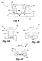
- a representative re-entrant photoresist profile 80 produced in accordance with a method of the present invention is shown.
- the photoresist profile 80 is formed once again upon a substrate 82 presenting a major surface 84 thereof.
- Photoresist 86 is patterned on the major surface 84 and, in accordance with the technique disclosed herein, a cap portion 88 is formed overlying a pedestal portion 90.
- FIGs. 5A-5C some representative re-entrant photoresist profiles 80 are shown produced in accordance with the foregoing equations (and corresponding to the entries in the preceding Table 1) to produce an active MR region of an MR head utilizing a conventional MRS structure to be followed by a self-aligned PM film sputtering step.
- the structure corresponding to that previously described with respect to Fig. 4 is like numbered and the foregoing description thereof shall suffice herefor.
- the method of the present invention is applicable to any thin film processing application utilizing photoresist wherein a re-entrant (or undercut) profile is desirably provided to facilitate subsequent removal of the photoresist by means of a suitable solvent.
Landscapes
- Physics & Mathematics (AREA)
- General Physics & Mathematics (AREA)
- Engineering & Computer Science (AREA)
- Manufacturing & Machinery (AREA)
- Electromagnetism (AREA)
- Magnetic Heads (AREA)
- Hall/Mr Elements (AREA)
- Photosensitive Polymer And Photoresist Processing (AREA)
Applications Claiming Priority (2)
| Application Number | Priority Date | Filing Date | Title |
|---|---|---|---|
| US570487 | 1984-01-13 | ||
| US08/570,487 US5658469A (en) | 1995-12-11 | 1995-12-11 | Method for forming re-entrant photoresist lift-off profile for thin film device processing and a thin film device made thereby |
Publications (2)
| Publication Number | Publication Date |
|---|---|
| EP0779557A2 true EP0779557A2 (de) | 1997-06-18 |
| EP0779557A3 EP0779557A3 (de) | 1998-11-18 |
Family
ID=24279843
Family Applications (1)
| Application Number | Title | Priority Date | Filing Date |
|---|---|---|---|
| EP96308492A Withdrawn EP0779557A3 (de) | 1995-12-11 | 1996-11-25 | Verfahren zur Erzeugung eines überhängenden lift-off Resistprofils zur Herstellung von Dünnschichtelementen und ein derart erzeugtes Dünnschichtelement |
Country Status (8)
| Country | Link |
|---|---|
| US (1) | US5658469A (de) |
| EP (1) | EP0779557A3 (de) |
| JP (1) | JPH09185814A (de) |
| KR (1) | KR970050298A (de) |
| CN (1) | CN1157479A (de) |
| AU (1) | AU7182096A (de) |
| CA (1) | CA2190712A1 (de) |
| SG (1) | SG44065A1 (de) |
Cited By (3)
| Publication number | Priority date | Publication date | Assignee | Title |
|---|---|---|---|---|
| WO2003043062A1 (en) * | 2001-11-10 | 2003-05-22 | Trikon Holdings Limited | Method of forming a patterned metal layer |
| WO2003046664A3 (en) * | 2001-11-28 | 2003-12-24 | Unaxis Balzers Ltd | Lithography process for transparent substrates |
| US6933099B2 (en) | 2001-11-10 | 2005-08-23 | Trikon Holdings Limited | Method of forming a patterned metal layer |
Families Citing this family (32)
| Publication number | Priority date | Publication date | Assignee | Title |
|---|---|---|---|---|
| US5930084A (en) * | 1996-06-17 | 1999-07-27 | International Business Machines Corporation | Stabilized MR sensor and flux guide joined by contiguous junction |
| JP3473931B2 (ja) | 1996-11-11 | 2003-12-08 | 東京応化工業株式会社 | リフトオフ用ポジ型感光性組成物およびパターン形成方法 |
| US5804085A (en) * | 1997-01-30 | 1998-09-08 | Quantum Corporation | Process for producing a pole-trimmed writer in a magnetoresistive read/write head and a data transducer made thereby |
| JPH11175920A (ja) * | 1997-12-05 | 1999-07-02 | Nec Corp | 磁気抵抗効果型複合ヘッドおよびその製造方法 |
| KR100540644B1 (ko) * | 1998-02-19 | 2006-02-28 | 삼성전자주식회사 | 마이크로 엑츄에이터 제조방법 |
| US6007731A (en) * | 1998-03-23 | 1999-12-28 | Headway Technologies, Inc. | Soft adjacent layer (SAL) magnetoresistive (MR) sensor element with electrically insulated soft adjacent layer (SAL) |
| JP2000056469A (ja) * | 1998-08-06 | 2000-02-25 | Tdk Corp | レジストパターンの形成方法 |
| US6156487A (en) | 1998-10-23 | 2000-12-05 | Matsushita-Kotobuki Electronics Industries, Ltd. | Top surface imaging technique for top pole tip width control in magnetoresistive read/write head processing |
| US6228276B1 (en) * | 1999-02-05 | 2001-05-08 | Headway Technologies, Inc. | Method of manufacturing magnetoresistive (MR) sensor element with sunken lead structure |
| US6218090B1 (en) | 1999-03-17 | 2001-04-17 | Electron Vision Corporation | Method of creating controlled discontinuity between photoresist and substrate for improving metal lift off |
| US6255035B1 (en) | 1999-03-17 | 2001-07-03 | Electron Vision Corporation | Method of creating optimal photoresist structures used in the manufacture of metal T-gates for high-speed semiconductor devices |
| US6445553B2 (en) | 1999-04-02 | 2002-09-03 | Read-Rite Corporation | Method and system for fabricating a high density magnetoresistive device |
| US6274025B1 (en) * | 1999-06-14 | 2001-08-14 | Headway Technologies, Inc. | Chemical approach to develop lift-off photoresist structure and passivate MR sensor |
| US6287476B1 (en) | 1999-06-14 | 2001-09-11 | Headway Technologies, Inc. | Electrochemical method to improve MR reader edge definition and device reliability |
| US6469877B1 (en) | 1999-06-15 | 2002-10-22 | Read-Rite Corporation | Spin valve device with improved exchange layer defined track width and method of fabrication |
| JP3348702B2 (ja) * | 1999-08-26 | 2002-11-20 | ティーディーケイ株式会社 | レジストパターンの形成方法及び薄膜素子の製造方法 |
| US6303416B1 (en) * | 1999-10-07 | 2001-10-16 | International Business Machines Corporation | Method to reduce plasma etch fluting |
| US6524689B1 (en) | 1999-10-28 | 2003-02-25 | Quantum Corporation | Castellation technique for improved lift-off of photoresist in thin-film device processing and a thin-film device made thereby |
| US6430806B1 (en) | 2000-06-23 | 2002-08-13 | Read-Rite Corporation | Method for manufacturing an inductive write element employing bi-layer photoresist to define a thin high moment pole pedestal |
| US6798622B2 (en) | 2000-12-11 | 2004-09-28 | Headway Technologies, Inc. | Magnetoresistive (MR) sensor element with sunken lead structure |
| US6828259B2 (en) * | 2001-03-28 | 2004-12-07 | Advanced Micro Devices, Inc. | Enhanced transistor gate using E-beam radiation |
| US6716571B2 (en) * | 2001-03-28 | 2004-04-06 | Advanced Micro Devices, Inc. | Selective photoresist hardening to facilitate lateral trimming |
| US6630288B2 (en) * | 2001-03-28 | 2003-10-07 | Advanced Micro Devices, Inc. | Process for forming sub-lithographic photoresist features by modification of the photoresist surface |
| JP3883004B2 (ja) * | 2002-12-25 | 2007-02-21 | Tdk株式会社 | パターン化薄膜形成方法およびマイクロデバイスの製造方法 |
| US7175876B2 (en) * | 2003-06-27 | 2007-02-13 | 3M Innovative Properties Company | Patterned coating method employing polymeric coatings |
| US6989327B2 (en) * | 2004-01-31 | 2006-01-24 | Hewlett-Packard Development Company, L.P. | Forming a contact in a thin-film device |
| ITMI20050616A1 (it) * | 2005-04-12 | 2006-10-13 | Getters Spa | Processo per la formazione di depositi getter miniaturizzati e depositi getrter cosi'ottenuti |
| JP2008016467A (ja) * | 2006-07-03 | 2008-01-24 | Fujitsu Ltd | パターン製造方法 |
| CN100495216C (zh) * | 2006-09-22 | 2009-06-03 | 中国科学院微电子研究所 | 一种电子束对准标记的制作方法及其应用 |
| US8652339B1 (en) * | 2013-01-22 | 2014-02-18 | The United States Of America, As Represented By The Secretary Of The Navy | Patterned lift-off of thin films deposited at high temperatures |
| KR102255954B1 (ko) | 2013-10-22 | 2021-05-24 | 어플라이드 머티어리얼스, 인코포레이티드 | 포토레지스트 두께에 따라 라이팅 빔들의 전달 도즈를 변화시키기 위한 프로세서들을 이용하는 패턴 생성기들, 및 관련 방법들 |
| CN115356895B (zh) * | 2022-07-22 | 2025-08-19 | 华南师范大学 | 利用正负可调光刻胶特性一步制备微纳结构的系统及方法 |
Family Cites Families (2)
| Publication number | Priority date | Publication date | Assignee | Title |
|---|---|---|---|---|
| US5468595A (en) * | 1993-01-29 | 1995-11-21 | Electron Vision Corporation | Method for three-dimensional control of solubility properties of resist layers |
| US5467881A (en) * | 1994-06-28 | 1995-11-21 | International Business Machines Corporation | Method of manufacturing an MR read head which eliminates lead-to-shield shorts at the ABS of the MR read head |
-
1995
- 1995-12-11 US US08/570,487 patent/US5658469A/en not_active Expired - Fee Related
-
1996
- 1996-11-19 CA CA002190712A patent/CA2190712A1/en not_active Abandoned
- 1996-11-19 AU AU71820/96A patent/AU7182096A/en not_active Abandoned
- 1996-11-25 EP EP96308492A patent/EP0779557A3/de not_active Withdrawn
- 1996-11-30 SG SG1996011491A patent/SG44065A1/en unknown
- 1996-12-10 CN CN96119765A patent/CN1157479A/zh active Pending
- 1996-12-10 KR KR1019960063379A patent/KR970050298A/ko not_active Withdrawn
- 1996-12-10 JP JP8329461A patent/JPH09185814A/ja not_active Withdrawn
Cited By (4)
| Publication number | Priority date | Publication date | Assignee | Title |
|---|---|---|---|---|
| WO2003043062A1 (en) * | 2001-11-10 | 2003-05-22 | Trikon Holdings Limited | Method of forming a patterned metal layer |
| GB2404084A (en) * | 2001-11-10 | 2005-01-19 | Trikon Holdings Ltd | Method of forming a patterned metal layer |
| US6933099B2 (en) | 2001-11-10 | 2005-08-23 | Trikon Holdings Limited | Method of forming a patterned metal layer |
| WO2003046664A3 (en) * | 2001-11-28 | 2003-12-24 | Unaxis Balzers Ltd | Lithography process for transparent substrates |
Also Published As
| Publication number | Publication date |
|---|---|
| CA2190712A1 (en) | 1997-06-12 |
| JPH09185814A (ja) | 1997-07-15 |
| AU7182096A (en) | 1997-06-19 |
| CN1157479A (zh) | 1997-08-20 |
| KR970050298A (ko) | 1997-07-29 |
| EP0779557A3 (de) | 1998-11-18 |
| SG44065A1 (en) | 1997-11-14 |
| US5658469A (en) | 1997-08-19 |
Similar Documents
| Publication | Publication Date | Title |
|---|---|---|
| US5658469A (en) | Method for forming re-entrant photoresist lift-off profile for thin film device processing and a thin film device made thereby | |
| US4098917A (en) | Method of providing a patterned metal layer on a substrate employing metal mask and ion milling | |
| EP0341843A2 (de) | Verfahren zur Herstellung eines Leitermusters | |
| CA1071761A (en) | Method for making multilayer devices using only a single critical masking step | |
| US4597826A (en) | Method for forming patterns | |
| US4337132A (en) | Ion etching process with minimized redeposition | |
| EP0384145B1 (de) | Feinstruktur-Litographieverfahren unter Verwendung von Fotolackschichten und einer plattierten Transferschicht | |
| US6569578B2 (en) | Method for forming photo-mask | |
| US4826754A (en) | Method for anisotropically hardening a protective coating for integrated circuit manufacture | |
| JP3100582B2 (ja) | 走査型電子顕微鏡及びパターン測定方法 | |
| JPH0620903A (ja) | 半導体装置の製造方法 | |
| JP2867248B2 (ja) | 位相シフトマスクの製造方法 | |
| WO1988003703A1 (en) | Multilayer resist structure | |
| JP3146685B2 (ja) | ゲート電極の形成方法 | |
| JP2752022B2 (ja) | 微細パターン形成方法 | |
| JP2785315B2 (ja) | 微細パターンの形成方法 | |
| JPS627688B2 (de) | ||
| JPH0191421A (ja) | パターン形成方法 | |
| JPH0744148B2 (ja) | 両面吸収体x線マスクの製造方法 | |
| JPH02119220A (ja) | 半導体装置の製造方法 | |
| JPH05241350A (ja) | レジストパターン形成方法 | |
| JPS60236235A (ja) | 半導体のパタ−ニング方法 | |
| JPH046284A (ja) | 薄膜パターンの形成方法 | |
| JPS5941832A (ja) | 位置検出用マ−クの形成方法 | |
| JPH02210827A (ja) | パターン形成方法 |
Legal Events
| Date | Code | Title | Description |
|---|---|---|---|
| PUAI | Public reference made under article 153(3) epc to a published international application that has entered the european phase |
Free format text: ORIGINAL CODE: 0009012 |
|
| AK | Designated contracting states |
Kind code of ref document: A2 Designated state(s): DE FR GB IT NL |
|
| PUAL | Search report despatched |
Free format text: ORIGINAL CODE: 0009013 |
|
| AK | Designated contracting states |
Kind code of ref document: A3 Designated state(s): DE FR GB IT NL |
|
| 17P | Request for examination filed |
Effective date: 19981204 |
|
| 17Q | First examination report despatched |
Effective date: 19990618 |
|
| STAA | Information on the status of an ep patent application or granted ep patent |
Free format text: STATUS: THE APPLICATION IS DEEMED TO BE WITHDRAWN |
|
| 18D | Application deemed to be withdrawn |
Effective date: 19991229 |