EP0782023B1 - Module émetteur-récepteur optique - Google Patents
Module émetteur-récepteur optique Download PDFInfo
- Publication number
- EP0782023B1 EP0782023B1 EP96120996A EP96120996A EP0782023B1 EP 0782023 B1 EP0782023 B1 EP 0782023B1 EP 96120996 A EP96120996 A EP 96120996A EP 96120996 A EP96120996 A EP 96120996A EP 0782023 B1 EP0782023 B1 EP 0782023B1
- Authority
- EP
- European Patent Office
- Prior art keywords
- optical
- waveguide
- substrate
- optical waveguide
- receiver module
- Prior art date
- Legal status (The legal status is an assumption and is not a legal conclusion. Google has not performed a legal analysis and makes no representation as to the accuracy of the status listed.)
- Expired - Lifetime
Links
- 230000003287 optical effect Effects 0.000 title claims description 226
- 239000000758 substrate Substances 0.000 claims description 47
- 239000013307 optical fiber Substances 0.000 claims description 22
- 239000004065 semiconductor Substances 0.000 description 47
- 230000005540 biological transmission Effects 0.000 description 11
- 238000000034 method Methods 0.000 description 10
- 230000002457 bidirectional effect Effects 0.000 description 5
- 230000003247 decreasing effect Effects 0.000 description 4
- 238000004519 manufacturing process Methods 0.000 description 4
- 238000005452 bending Methods 0.000 description 3
- 230000002542 deteriorative effect Effects 0.000 description 3
- 239000000835 fiber Substances 0.000 description 3
- 239000000203 mixture Substances 0.000 description 3
- 238000012544 monitoring process Methods 0.000 description 2
- 229910052782 aluminium Inorganic materials 0.000 description 1
- 238000010276 construction Methods 0.000 description 1
- 230000008878 coupling Effects 0.000 description 1
- 238000010168 coupling process Methods 0.000 description 1
- 238000005859 coupling reaction Methods 0.000 description 1
- 239000006185 dispersion Substances 0.000 description 1
- 229910052737 gold Inorganic materials 0.000 description 1
- 230000010354 integration Effects 0.000 description 1
- 230000004048 modification Effects 0.000 description 1
- 238000012986 modification Methods 0.000 description 1
- 238000005498 polishing Methods 0.000 description 1
- 229910052709 silver Inorganic materials 0.000 description 1
- 239000000126 substance Substances 0.000 description 1
Images


Classifications
-
- G—PHYSICS
- G02—OPTICS
- G02B—OPTICAL ELEMENTS, SYSTEMS OR APPARATUS
- G02B6/00—Light guides; Structural details of arrangements comprising light guides and other optical elements, e.g. couplings
- G02B6/24—Coupling light guides
- G02B6/42—Coupling light guides with opto-electronic elements
- G02B6/4201—Packages, e.g. shape, construction, internal or external details
- G02B6/4246—Bidirectionally operating package structures
Definitions
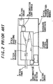
- This invention relates to an optical transmitter-receiver module, and more particularly to, an optical transmitter-receiver module which is used in a bidirectional optical transmission system.
Landscapes
- Physics & Mathematics (AREA)
- General Physics & Mathematics (AREA)
- Optics & Photonics (AREA)
- Optical Integrated Circuits (AREA)
- Optical Couplings Of Light Guides (AREA)
Claims (4)
- Module émetteur-récepteur optique (9),
dans lequel un dispositif optique de guides d'ondes (2) ramifie un seul guide d'onde à une première extrémité du substrat (1) à deux guides d'ondes (2a, 2b) à la deuxième extrémité du substrat (1), et le côté ramifié dudit guide d'onde optique (2) soit relié optiquement à une fibre optique (4) à ladite première extrémité du substrat dudit premier guide d'onde (1),
et dans lequel à l'extrémité d'un (2b) des deux guides d'ondes sur le côté ramifié dudit guide d'onde optique (2) un réflecteur (8) soit placé à la deuxième extrémité dudit substrat de guide d'onde (1), et un guide d'onde optique supplémentaire (7) s'étende depuis la deuxième extrémité dudit substrat de guide d'onde à la première extrémité dudit substrat de guide d'onde (1), ledit réflecteur (8) reliant optiquement ladite deuxième branche de guide d'onde (2b) audit guide d'onde optique supplémentaire (7),
un émetteur optique (5a, 5b) et un récepteur optique (6a, 6b) étant relié optiquement à l'autre (2a) desdits deux guides d'ondes optiques (2a, 2b) sur le côté ramifié dudit guide d'onde optique (2) à ladite deuxième extrémité dudit substrat de guide d'onde (1) et audit guide d'onde optique(7) supplémentaire à ladite première extrémité du substrat dudit guide d'onde (1),
caractérisé en ce que l'autre (2a) desdits deux guides d'ondes optiques (2a, 2b) sur le côté ramifié dudit guide d'onde optique (2) soit relié optiquement audit récepteur optique (6a, 6b) à ladite deuxième extrémité dudit substrat de guide d'onde (1), et ledit guide d'onde optique supplémentaire (7) soit connecté optiquement audit émetteur optique (5a, 5b) à ladite première extrémité du substrat dudit guide d'onde. - Module émetteur-récepteur optique (9) selon la revendication 1, caractérisé en ce que ledit second guide d'onde optique (2b) et ledit guide d'onde optique supplémentaire (7) soient disposés rapprochés sur ladite deuxième extrémité dudit substrat de guide d'onde et soient formés comme coupleur directionnel optique dans lequel ils sont reliés optiquement en utilisant un moyen réflecteur (8) disposé sur une surface d'extrémité de ladite deuxième extrémité du substrat dudit guide d'onde.
- Module émetteur-récepteur optique (9), selon la revendication 1 ou 2 où:l'espacement dudit second guide d'onde optique (2b) et dudit guide d'onde optique supplémentaire (7) dans ledit coupleur optique directionnel soit réglé sur 4 µm ou moins.
- Module émetteur-récepteur optique (9), selon l'une des revendications 1 à 3, où:un autre guide d'onde optique soit disposé afin de former un multiplexeur-démultiplexeur optique avec ledit côté non-ramifié dudit guide d'onde optique (2) et ledit autre guide d'onde optique soit relié optiquement à une autre fibre optique.
Applications Claiming Priority (3)
| Application Number | Priority Date | Filing Date | Title |
|---|---|---|---|
| JP7353483A JP2919329B2 (ja) | 1995-12-30 | 1995-12-30 | 光送受信モジュール |
| JP353483/95 | 1995-12-30 | ||
| JP35348395 | 1995-12-30 |
Publications (3)
| Publication Number | Publication Date |
|---|---|
| EP0782023A2 EP0782023A2 (fr) | 1997-07-02 |
| EP0782023A3 EP0782023A3 (fr) | 1998-12-16 |
| EP0782023B1 true EP0782023B1 (fr) | 2002-03-27 |
Family
ID=18431153
Family Applications (1)
| Application Number | Title | Priority Date | Filing Date |
|---|---|---|---|
| EP96120996A Expired - Lifetime EP0782023B1 (fr) | 1995-12-30 | 1996-12-30 | Module émetteur-récepteur optique |
Country Status (4)
| Country | Link |
|---|---|
| US (1) | US5825951A (fr) |
| EP (1) | EP0782023B1 (fr) |
| JP (1) | JP2919329B2 (fr) |
| DE (1) | DE69620130T2 (fr) |
Families Citing this family (22)
| Publication number | Priority date | Publication date | Assignee | Title |
|---|---|---|---|---|
| JP3355122B2 (ja) * | 1998-01-08 | 2002-12-09 | 富士通株式会社 | 光モジュールの封止方法 |
| JPH11237517A (ja) * | 1998-02-23 | 1999-08-31 | Fujitsu Ltd | 光導波路素子 |
| SE524892C2 (sv) * | 1998-03-06 | 2004-10-19 | Ericsson Telefon Ab L M | Provning av optiska sändar- och mottagarmoduler |
| US6175670B1 (en) * | 1998-03-23 | 2001-01-16 | Lucent Technologies, Inc. | Planar lightguide circuit having a planar grating |
| JPH11352341A (ja) * | 1998-06-04 | 1999-12-24 | Nec Corp | 導波路型波長多重光送受信モジュール |
| US6304695B1 (en) * | 1999-05-17 | 2001-10-16 | Chiaro Networks Ltd. | Modulated light source |
| JP2001108847A (ja) * | 1999-10-07 | 2001-04-20 | Mitsubishi Electric Corp | 光モジュール |
| US7606608B2 (en) | 2000-05-02 | 2009-10-20 | Sensys Medical, Inc. | Optical sampling interface system for in-vivo measurement of tissue |
| US20060211931A1 (en) * | 2000-05-02 | 2006-09-21 | Blank Thomas B | Noninvasive analyzer sample probe interface method and apparatus |
| US7519406B2 (en) * | 2004-04-28 | 2009-04-14 | Sensys Medical, Inc. | Noninvasive analyzer sample probe interface method and apparatus |
| WO2002010826A1 (fr) * | 2000-07-31 | 2002-02-07 | Corning Incorporated | Reseaux de bragg internes de substrat et dispositifs optiques |
| WO2003027735A1 (fr) * | 2001-09-14 | 2003-04-03 | Infineon Technologies Ag | Dispositif optique et module emetteur/recepteur destine a des systemes wdm optiques bidirectionnels et a des transmissions de donnees optiques |
| KR100481578B1 (ko) * | 2002-09-18 | 2005-04-08 | 포테나 옵틱스 코포레이션 | 단일 광섬유를 이용한 양방향 광송수신 모듈 및 그에사용되는 광도파로 거치대 |
| US7229763B2 (en) * | 2003-04-07 | 2007-06-12 | Beckman Coulter, Inc. | Assay system using labeled oligonucleotides |
| KR20040104813A (ko) * | 2003-06-04 | 2004-12-13 | 삼성전자주식회사 | 양방향 광송수신기 모듈 |
| US7492992B1 (en) * | 2003-08-08 | 2009-02-17 | Neophotonics Corporation | Bi-directional PLC transceiver device |
| KR100659587B1 (ko) | 2004-09-22 | 2006-12-20 | 한국전자통신연구원 | 삼 파장 광 송수신 모듈 및 그 제조방법 |
| FR2886762B1 (fr) * | 2005-06-07 | 2007-08-10 | Commissariat Energie Atomique | Detecteur optique ultrasensible, a grande resolution temporelle, utilisant un guide d'onde, et procedes de fabrication de ce detecteur |
| GB0512386D0 (en) * | 2005-06-17 | 2005-07-27 | Ct For Integrated Photonics Th | Folded cavity optoelectronic devices |
| JP5180963B2 (ja) * | 2006-09-07 | 2013-04-10 | マグナコースティックス インコーポレイテッド | 医療画像システムにおけるスキャンの起動 |
| US20090036759A1 (en) * | 2007-08-01 | 2009-02-05 | Ault Timothy E | Collapsible noninvasive analyzer method and apparatus |
| EP2981010B1 (fr) * | 2013-06-24 | 2018-04-25 | Huawei Technologies Co., Ltd. | Module optique et système de reseau optique |
Family Cites Families (14)
| Publication number | Priority date | Publication date | Assignee | Title |
|---|---|---|---|---|
| DE3881252D1 (de) * | 1987-03-30 | 1993-07-01 | Siemens Ag | Integriert-optische anordnung fuer die bidirektionale optische nachrichten- oder signaluebertragung. |
| JPH03223705A (ja) * | 1989-12-12 | 1991-10-02 | Hitachi Cable Ltd | 光合分波器及び光合分波器モジュール |
| US5016960A (en) * | 1989-12-22 | 1991-05-21 | Gte Laboratories Incorporated | Hybrid optical Y-junction |
| JP2631902B2 (ja) * | 1990-04-20 | 1997-07-16 | 日本航空電子工業 株式会社 | 光集積回路 |
| JPH0481104A (ja) * | 1990-07-23 | 1992-03-13 | Hitachi Ferrite Ltd | 誘電体共振器 |
| JPH0481104U (fr) * | 1990-11-28 | 1992-07-15 | ||
| JP2579092B2 (ja) * | 1991-11-21 | 1997-02-05 | 日立電線株式会社 | 双方向光伝送用wdmモジュ−ル |
| JPH0634833A (ja) * | 1992-07-13 | 1994-02-10 | Mitsubishi Gas Chem Co Inc | 光送受信用部品 |
| US5361157A (en) * | 1992-08-25 | 1994-11-01 | Nippon Hoso Kyokai | Bidirectional light transmission system and optical device therefor |
| JPH0697561A (ja) * | 1992-09-14 | 1994-04-08 | Hitachi Cable Ltd | 導波路型双方向伝送モジュールの光出力安定化方式 |
| US5333219A (en) * | 1992-12-17 | 1994-07-26 | At&T Bell Laboratories | Asymmetric Y-branch optical device |
| DE69415768T2 (de) * | 1993-11-01 | 1999-06-10 | Sumitomo Electric Industries, Ltd., Osaka | Optisches Abzweigelement |
| JP2867859B2 (ja) * | 1993-12-13 | 1999-03-10 | 日本電気株式会社 | 双方向伝送用光送受信モジュール |
| JPH0915436A (ja) * | 1995-06-27 | 1997-01-17 | Fujitsu Ltd | 光導波路構造並びに光分波器,光合波器,光選別器及び光合波・分波器 |
-
1995
- 1995-12-30 JP JP7353483A patent/JP2919329B2/ja not_active Expired - Fee Related
-
1996
- 1996-12-30 EP EP96120996A patent/EP0782023B1/fr not_active Expired - Lifetime
- 1996-12-30 US US08/775,183 patent/US5825951A/en not_active Expired - Fee Related
- 1996-12-30 DE DE69620130T patent/DE69620130T2/de not_active Expired - Lifetime
Also Published As
| Publication number | Publication date |
|---|---|
| EP0782023A3 (fr) | 1998-12-16 |
| US5825951A (en) | 1998-10-20 |
| JP2919329B2 (ja) | 1999-07-12 |
| DE69620130D1 (de) | 2002-05-02 |
| JPH09184934A (ja) | 1997-07-15 |
| DE69620130T2 (de) | 2002-08-29 |
| EP0782023A2 (fr) | 1997-07-02 |
Similar Documents
| Publication | Publication Date | Title |
|---|---|---|
| EP0782023B1 (fr) | Module émetteur-récepteur optique | |
| US5499309A (en) | Method of fabricating optical component including first and second optical waveguide chips having opposed inclined surfaces | |
| US5497438A (en) | Optical transmission and reception module having coupled optical waveguide chips | |
| US6744945B2 (en) | Wavelength multiplexer and optical unit | |
| US6572278B2 (en) | Opto-electronic device having staked connection between parts to prevent differential thermal expansion | |
| JP3092499B2 (ja) | 導波路型光合波分波モジュール | |
| JP2867859B2 (ja) | 双方向伝送用光送受信モジュール | |
| US6741776B2 (en) | Optical waveguide module optically connected with an optical fiber | |
| JP2002131586A (ja) | 光通信モジュールとその製造方法 | |
| US6408121B1 (en) | Optical communication module | |
| CA2634293A1 (fr) | Lentille thermo-optique accordable, integree, multicanaux et compensateur de dispersion | |
| US6937779B2 (en) | Optical module | |
| US6507680B1 (en) | Planar lightwave circuit module | |
| CN115407434A (zh) | 光次组件模组中使用的抛物面透镜装置 | |
| US20020071633A1 (en) | Wavelength multiplex optical communication module | |
| US20070110363A1 (en) | Optical system with optical waveguides | |
| WO2002019002A1 (fr) | Ferrule de fibre optique munie d'un polariseur, connecteur et adaptateur de connecteur | |
| EP1496377A2 (fr) | Multiplexeur / démultiplexeur optique, circuit intégré optique et émetteur-récepteur utilisant les mêmes | |
| JP2003519823A (ja) | 光学的カップリングシステム | |
| JPH05203830A (ja) | 光合分波器 | |
| US5432338A (en) | Silicon opto-electronic integrated circuit for fiber optic gyros or communication | |
| EP2031427B1 (fr) | Terminal optique | |
| JP3120774B2 (ja) | 光送受信モジュール及びその製造方法 | |
| JP2865789B2 (ja) | 光伝送モジュール | |
| EP1233487B1 (fr) | Module optique à semi-conducteur avec dispositif de surveillance de lumière pour surveiller le signal lumineux émis par un élément émetteur de lumière |
Legal Events
| Date | Code | Title | Description |
|---|---|---|---|
| PUAI | Public reference made under article 153(3) epc to a published international application that has entered the european phase |
Free format text: ORIGINAL CODE: 0009012 |
|
| AK | Designated contracting states |
Kind code of ref document: A2 Designated state(s): DE GB |
|
| PUAL | Search report despatched |
Free format text: ORIGINAL CODE: 0009013 |
|
| AK | Designated contracting states |
Kind code of ref document: A3 Designated state(s): DE GB |
|
| 17P | Request for examination filed |
Effective date: 19990301 |
|
| 17Q | First examination report despatched |
Effective date: 19990906 |
|
| GRAG | Despatch of communication of intention to grant |
Free format text: ORIGINAL CODE: EPIDOS AGRA |
|
| GRAG | Despatch of communication of intention to grant |
Free format text: ORIGINAL CODE: EPIDOS AGRA |
|
| GRAH | Despatch of communication of intention to grant a patent |
Free format text: ORIGINAL CODE: EPIDOS IGRA |
|
| GRAH | Despatch of communication of intention to grant a patent |
Free format text: ORIGINAL CODE: EPIDOS IGRA |
|
| REG | Reference to a national code |
Ref country code: GB Ref legal event code: IF02 |
|
| GRAA | (expected) grant |
Free format text: ORIGINAL CODE: 0009210 |
|
| AK | Designated contracting states |
Kind code of ref document: B1 Designated state(s): DE GB |
|
| REF | Corresponds to: |
Ref document number: 69620130 Country of ref document: DE Date of ref document: 20020502 |
|
| PLBE | No opposition filed within time limit |
Free format text: ORIGINAL CODE: 0009261 |
|
| STAA | Information on the status of an ep patent application or granted ep patent |
Free format text: STATUS: NO OPPOSITION FILED WITHIN TIME LIMIT |
|
| 26N | No opposition filed |
Effective date: 20021230 |
|
| PGFP | Annual fee paid to national office [announced via postgrant information from national office to epo] |
Ref country code: GB Payment date: 20151230 Year of fee payment: 20 |
|
| PGFP | Annual fee paid to national office [announced via postgrant information from national office to epo] |
Ref country code: DE Payment date: 20151222 Year of fee payment: 20 |
|
| REG | Reference to a national code |
Ref country code: DE Ref legal event code: R071 Ref document number: 69620130 Country of ref document: DE |
|
| REG | Reference to a national code |
Ref country code: GB Ref legal event code: PE20 Expiry date: 20161229 |
|
| PG25 | Lapsed in a contracting state [announced via postgrant information from national office to epo] |
Ref country code: GB Free format text: LAPSE BECAUSE OF EXPIRATION OF PROTECTION Effective date: 20161229 |