EP0786806A1 - Boîtier d'entrées/sorties à haute densité pour des puces de puissance à circuits intégrés avec des fils soudés et procédé de fabrication - Google Patents
Boîtier d'entrées/sorties à haute densité pour des puces de puissance à circuits intégrés avec des fils soudés et procédé de fabrication Download PDFInfo
- Publication number
- EP0786806A1 EP0786806A1 EP96480005A EP96480005A EP0786806A1 EP 0786806 A1 EP0786806 A1 EP 0786806A1 EP 96480005 A EP96480005 A EP 96480005A EP 96480005 A EP96480005 A EP 96480005A EP 0786806 A1 EP0786806 A1 EP 0786806A1
- Authority
- EP
- European Patent Office
- Prior art keywords
- active surface
- substrate
- package
- cavity
- bonded
- Prior art date
- Legal status (The legal status is an assumption and is not a legal conclusion. Google has not performed a legal analysis and makes no representation as to the accuracy of the status listed.)
- Withdrawn
Links
Images

Classifications
-
- H—ELECTRICITY
- H10—SEMICONDUCTOR DEVICES; ELECTRIC SOLID-STATE DEVICES NOT OTHERWISE PROVIDED FOR
- H10W—GENERIC PACKAGES, INTERCONNECTIONS, CONNECTORS OR OTHER CONSTRUCTIONAL DETAILS OF DEVICES COVERED BY CLASS H10
- H10W40/00—Arrangements for thermal protection or thermal control
- H10W40/20—Arrangements for cooling
- H10W40/22—Arrangements for cooling characterised by their shape, e.g. having conical or cylindrical projections
- H10W40/226—Arrangements for cooling characterised by their shape, e.g. having conical or cylindrical projections characterised by projecting parts, e.g. fins to increase surface area
- H10W40/228—Arrangements for cooling characterised by their shape, e.g. having conical or cylindrical projections characterised by projecting parts, e.g. fins to increase surface area the projecting parts being wire-shaped or pin-shaped
-
- H—ELECTRICITY
- H10—SEMICONDUCTOR DEVICES; ELECTRIC SOLID-STATE DEVICES NOT OTHERWISE PROVIDED FOR
- H10W—GENERIC PACKAGES, INTERCONNECTIONS, CONNECTORS OR OTHER CONSTRUCTIONAL DETAILS OF DEVICES COVERED BY CLASS H10
- H10W40/00—Arrangements for thermal protection or thermal control
- H10W40/70—Fillings or auxiliary members in containers or in encapsulations for thermal protection or control
- H10W40/77—Auxiliary members characterised by their shape
-
- H—ELECTRICITY
- H10—SEMICONDUCTOR DEVICES; ELECTRIC SOLID-STATE DEVICES NOT OTHERWISE PROVIDED FOR
- H10W—GENERIC PACKAGES, INTERCONNECTIONS, CONNECTORS OR OTHER CONSTRUCTIONAL DETAILS OF DEVICES COVERED BY CLASS H10
- H10W72/00—Interconnections or connectors in packages
- H10W72/30—Die-attach connectors
-
- H—ELECTRICITY
- H10—SEMICONDUCTOR DEVICES; ELECTRIC SOLID-STATE DEVICES NOT OTHERWISE PROVIDED FOR
- H10W—GENERIC PACKAGES, INTERCONNECTIONS, CONNECTORS OR OTHER CONSTRUCTIONAL DETAILS OF DEVICES COVERED BY CLASS H10
- H10W70/00—Package substrates; Interposers; Redistribution layers [RDL]
- H10W70/60—Insulating or insulated package substrates; Interposers; Redistribution layers
- H10W70/67—Insulating or insulated package substrates; Interposers; Redistribution layers characterised by their insulating layers or insulating parts
- H10W70/68—Shapes or dispositions thereof
- H10W70/682—Shapes or dispositions thereof comprising holes having chips therein
-
- H—ELECTRICITY
- H10—SEMICONDUCTOR DEVICES; ELECTRIC SOLID-STATE DEVICES NOT OTHERWISE PROVIDED FOR
- H10W—GENERIC PACKAGES, INTERCONNECTIONS, CONNECTORS OR OTHER CONSTRUCTIONAL DETAILS OF DEVICES COVERED BY CLASS H10
- H10W72/00—Interconnections or connectors in packages
- H10W72/01—Manufacture or treatment
- H10W72/013—Manufacture or treatment of die-attach connectors
- H10W72/01308—Manufacture or treatment of die-attach connectors using permanent auxiliary members, e.g. using alignment marks
-
- H—ELECTRICITY
- H10—SEMICONDUCTOR DEVICES; ELECTRIC SOLID-STATE DEVICES NOT OTHERWISE PROVIDED FOR
- H10W—GENERIC PACKAGES, INTERCONNECTIONS, CONNECTORS OR OTHER CONSTRUCTIONAL DETAILS OF DEVICES COVERED BY CLASS H10
- H10W72/00—Interconnections or connectors in packages
- H10W72/01—Manufacture or treatment
- H10W72/015—Manufacture or treatment of bond wires
- H10W72/01515—Forming coatings
-
- H—ELECTRICITY
- H10—SEMICONDUCTOR DEVICES; ELECTRIC SOLID-STATE DEVICES NOT OTHERWISE PROVIDED FOR
- H10W—GENERIC PACKAGES, INTERCONNECTIONS, CONNECTORS OR OTHER CONSTRUCTIONAL DETAILS OF DEVICES COVERED BY CLASS H10
- H10W72/00—Interconnections or connectors in packages
- H10W72/071—Connecting or disconnecting
- H10W72/073—Connecting or disconnecting of die-attach connectors
- H10W72/07311—Treating the bonding area before connecting, e.g. by applying flux or cleaning
-
- H—ELECTRICITY
- H10—SEMICONDUCTOR DEVICES; ELECTRIC SOLID-STATE DEVICES NOT OTHERWISE PROVIDED FOR
- H10W—GENERIC PACKAGES, INTERCONNECTIONS, CONNECTORS OR OTHER CONSTRUCTIONAL DETAILS OF DEVICES COVERED BY CLASS H10
- H10W72/00—Interconnections or connectors in packages
- H10W72/071—Connecting or disconnecting
- H10W72/075—Connecting or disconnecting of bond wires
- H10W72/07541—Controlling the environment, e.g. atmosphere composition or temperature
- H10W72/07553—Controlling the environment, e.g. atmosphere composition or temperature changes in shapes
-
- H—ELECTRICITY
- H10—SEMICONDUCTOR DEVICES; ELECTRIC SOLID-STATE DEVICES NOT OTHERWISE PROVIDED FOR
- H10W—GENERIC PACKAGES, INTERCONNECTIONS, CONNECTORS OR OTHER CONSTRUCTIONAL DETAILS OF DEVICES COVERED BY CLASS H10
- H10W72/00—Interconnections or connectors in packages
- H10W72/50—Bond wires
- H10W72/531—Shapes of wire connectors
- H10W72/536—Shapes of wire connectors the connected ends being ball-shaped
-
- H—ELECTRICITY
- H10—SEMICONDUCTOR DEVICES; ELECTRIC SOLID-STATE DEVICES NOT OTHERWISE PROVIDED FOR
- H10W—GENERIC PACKAGES, INTERCONNECTIONS, CONNECTORS OR OTHER CONSTRUCTIONAL DETAILS OF DEVICES COVERED BY CLASS H10
- H10W72/00—Interconnections or connectors in packages
- H10W72/50—Bond wires
- H10W72/531—Shapes of wire connectors
- H10W72/5363—Shapes of wire connectors the connected ends being wedge-shaped
-
- H—ELECTRICITY
- H10—SEMICONDUCTOR DEVICES; ELECTRIC SOLID-STATE DEVICES NOT OTHERWISE PROVIDED FOR
- H10W—GENERIC PACKAGES, INTERCONNECTIONS, CONNECTORS OR OTHER CONSTRUCTIONAL DETAILS OF DEVICES COVERED BY CLASS H10
- H10W72/00—Interconnections or connectors in packages
- H10W72/50—Bond wires
- H10W72/541—Dispositions of bond wires
- H10W72/5445—Dispositions of bond wires being orthogonal to a side surface of the chip, e.g. parallel arrangements
-
- H—ELECTRICITY
- H10—SEMICONDUCTOR DEVICES; ELECTRIC SOLID-STATE DEVICES NOT OTHERWISE PROVIDED FOR
- H10W—GENERIC PACKAGES, INTERCONNECTIONS, CONNECTORS OR OTHER CONSTRUCTIONAL DETAILS OF DEVICES COVERED BY CLASS H10
- H10W72/00—Interconnections or connectors in packages
- H10W72/50—Bond wires
- H10W72/541—Dispositions of bond wires
- H10W72/5449—Dispositions of bond wires not being orthogonal to a side surface of the chip, e.g. fan-out arrangements
-
- H—ELECTRICITY
- H10—SEMICONDUCTOR DEVICES; ELECTRIC SOLID-STATE DEVICES NOT OTHERWISE PROVIDED FOR
- H10W—GENERIC PACKAGES, INTERCONNECTIONS, CONNECTORS OR OTHER CONSTRUCTIONAL DETAILS OF DEVICES COVERED BY CLASS H10
- H10W72/00—Interconnections or connectors in packages
- H10W72/851—Dispositions of multiple connectors or interconnections
- H10W72/853—On the same surface
- H10W72/865—Die-attach connectors and bond wires
-
- H—ELECTRICITY
- H10—SEMICONDUCTOR DEVICES; ELECTRIC SOLID-STATE DEVICES NOT OTHERWISE PROVIDED FOR
- H10W—GENERIC PACKAGES, INTERCONNECTIONS, CONNECTORS OR OTHER CONSTRUCTIONAL DETAILS OF DEVICES COVERED BY CLASS H10
- H10W72/00—Interconnections or connectors in packages
- H10W72/851—Dispositions of multiple connectors or interconnections
- H10W72/874—On different surfaces
- H10W72/884—Die-attach connectors and bond wires
-
- H—ELECTRICITY
- H10—SEMICONDUCTOR DEVICES; ELECTRIC SOLID-STATE DEVICES NOT OTHERWISE PROVIDED FOR
- H10W—GENERIC PACKAGES, INTERCONNECTIONS, CONNECTORS OR OTHER CONSTRUCTIONAL DETAILS OF DEVICES COVERED BY CLASS H10
- H10W72/00—Interconnections or connectors in packages
- H10W72/90—Bond pads, in general
- H10W72/931—Shapes of bond pads
-
- H—ELECTRICITY
- H10—SEMICONDUCTOR DEVICES; ELECTRIC SOLID-STATE DEVICES NOT OTHERWISE PROVIDED FOR
- H10W—GENERIC PACKAGES, INTERCONNECTIONS, CONNECTORS OR OTHER CONSTRUCTIONAL DETAILS OF DEVICES COVERED BY CLASS H10
- H10W72/00—Interconnections or connectors in packages
- H10W72/90—Bond pads, in general
- H10W72/951—Materials of bond pads
-
- H—ELECTRICITY
- H10—SEMICONDUCTOR DEVICES; ELECTRIC SOLID-STATE DEVICES NOT OTHERWISE PROVIDED FOR
- H10W—GENERIC PACKAGES, INTERCONNECTIONS, CONNECTORS OR OTHER CONSTRUCTIONAL DETAILS OF DEVICES COVERED BY CLASS H10
- H10W90/00—Package configurations
- H10W90/701—Package configurations characterised by the relative positions of pads or connectors relative to package parts
- H10W90/731—Package configurations characterised by the relative positions of pads or connectors relative to package parts of die-attach connectors
- H10W90/734—Package configurations characterised by the relative positions of pads or connectors relative to package parts of die-attach connectors between a chip and a stacked insulating package substrate, interposer or RDL
-
- H—ELECTRICITY
- H10—SEMICONDUCTOR DEVICES; ELECTRIC SOLID-STATE DEVICES NOT OTHERWISE PROVIDED FOR
- H10W—GENERIC PACKAGES, INTERCONNECTIONS, CONNECTORS OR OTHER CONSTRUCTIONAL DETAILS OF DEVICES COVERED BY CLASS H10
- H10W90/00—Package configurations
- H10W90/701—Package configurations characterised by the relative positions of pads or connectors relative to package parts
- H10W90/751—Package configurations characterised by the relative positions of pads or connectors relative to package parts of bond wires
- H10W90/754—Package configurations characterised by the relative positions of pads or connectors relative to package parts of bond wires between a chip and a stacked insulating package substrate, interposer or RDL
Definitions
- the present invention relates to packaging techniques for high power wire-bonded semiconductor integrated circuit chips and more particularly to a high I/O density package in which a cap (and/or a heat sink) is efficiently coupled to the active surface of the chip for improved heat dissipation without damaging the fragile bonding wires.
- FIG. 1 A cross section of a conventional cavity-up package is shown in Fig. 1 where it is indicated by reference numeral 10.
- a cavity-up (upward facing) substrate 11 is provided with a cavity 12 at its top side in which an IC chip 13 is attached by means of a layer 14 thermally conductive material (glue or eutectic solder).
- Bonding wires 15 make an electrical connection between the IC chip contact pads 16 and metal lands (not shown) formed at the surface of the substrate as standard. In turn, these metal lands are connected to input/output (I/O) terminals, typically solder balls/columns or pins 17, for external connections with conductors carried by a printed circuit board.
- I/O input/output
- the major problem with the cavity-up package 10 of Fig. 1 is that it is severely limited in its heat dissipating capabilities.
- the active surface of the IC chip (where heat is produced) is connected to air which is a poor thermal conductor.
- a heat sink is absolutely necessary. Without it, heat transfer would be very poor causing thereby irreparable damage to the IC chip.
- it is not possible to attach a heat sink to the substrate backside because of the presence of I/O's 17.
- a thermal compound such as a thermal grease
- dispensed between the heat sink and the IC chip active surface as it will now be illustrated by reference to Fig. 2, which focuses on the central portion of cavity-up package 10 of Fig. 1.
- An adequate material is Amicon S 4500 sold by GRACE, Westerlo, Belgium.
- the objective is twofold: the area of the active face covered by the grease layer has to be maximum (to reduce the ther mal resistance Rth) and the thickness of the grease layer between the said surface and the heat sink has to be minimum (to further reduce Rth).
- a radial spanning is not always achievable because the chip pad arrangement is defined by the IC chip manufacturer and the top substrate padding has to fit different constraints (e.g. module design ground rules). Therefore, as illustrated in Fig. 2, there has been no satisfactory solution known to date to thermally couple a cap or a heat sink to the active surface of a high power wire-bonded IC chip.
- a package referenced 20 comprised of downwards facing substrate 21 provided with a cavity 22 formed into its backside with IC chip 23 attached thereto by a thermally conductive layer 24 as explained above.
- the IC chip 23 is now upside-down. Bonding wires 25 interconnect the IC chip contact pads 26 to metal lands formed at the backside for transferring electrical signals to the I/O's 27.
- the heat sink 28 is attached to the top side of the substrate opposite to the cavity 22. This solution which allows an easy attachment of the heat sink 28 to the top side of substrate 21 has still some major inconveniences.
- the heat sink 28 must have larger dimensions that also favors an over-dimensioned substrate 21 footprint.
- the package footprint is the area occupied by the package on the printed circuit board which should be kept as small as possible so that more packages can be placed on the board.
- Rth thermal resistance
- the substrate 21 is made of a ceramic material (good Rth)
- the heat sink 28 can be attached directly to the top side of the substrate 21.
- the substrate 21 is made of an organic material (poor Rth)
- buried thermal vias shown in dotted lines in Fig. 3 are required to conduct the heat between the IC chip passive surface and the heat sink 28.
- a novel cavity-up (or flat) package having efficient heat dissipation capabilities adapted to high power wire-bonded IC chips and a method for making the same.
- the IC chip is upwardly mounted onto the substrate surface.
- the fragile bonding wires which interconnect the contact pads at the periphery of the IC chip and metal lands of the substrate are encapsulated in a material at contact pad locations.
- a ring-shaped stiffener which protects the bonding wire extremities for the subsequent steps.
- the stiffener forms a dam-like structure which delineates a recess substantially exposing the whole active surface (where heat is produced) of the IC chip.
- a cap (or a heat sink) is coupled to the IC chip active surface. It is provided with a mesa-shaped pedestal at its backside which fits well with said recess. It is firmly affixed onto the substrate so that the pedestal presses the grease down to the desired thickness for excellent heat transfer between the IC chip active surface and the cap. The cap is applied onto the substrate without damaging the fragile bonding wires thanks to the protection offered by the stiffener.
- the package fabricated according to this method keeps the inherent advantages of the so-called “cavity-up” or “flat” packaging techniques (high number of I/O's, small footprint) without its inherent inconveniences (low heat dissipation). It offers a very efficient heat dissipation scheme well adapted to any type of high power wire-bonded semiconductor IC chips (standard or radial wire spanning) without the risk of damaging said fragile bonding wires. It is also perfectly adapted to Multi-Chip-Module (MCM) technology.
- MCM Multi-Chip-Module
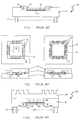
- Fig. 1 is a schematic cut-away side view of a typical cavity-up package of the prior art including a high power wire-bonded IC chip attached to the cavity bottom.
- Fig. 2 shows a top view of the package of Fig. 1 when a heat sink is applied onto the active surface of the IC chip with an intermediate thermal grease layer for better heat evacuation, either with a small quantity of grease in case of a standard wire spanning (A) or with a greater quantity of grease in case of a radial wire spanning (B).
- Fig. 3 is a schematic cut-away side view of a typical cavity-down package of the prior art still including a high power wire-bonded IC chip attached to the cavity bottom.
- Fig. 4 illustrates the step sequence of the method of fabricating the cavity-up package with improved heat dis sipation capabilities in accordance with the present in vention.
- the novel method is industrially oriented to wards high process yields and provides a high I/O density package with a very efficient heat dissipation scheme well adapted to high power wire-bonded IC chips.
- the basic idea is to encapsulate the extremities of bonding wires at contact pad locations with a stiffening material. After hardening, there is formed a ring-shaped stiffener at the periphery of the IC chip which (i) protects said extremities and (ii) delineates a recess in its interior space substantially exposing all the IC chip active surface.
- a thermal compound such as a thermal grease
- a cap having an interior shape that fits well with the recess is applied pressing the excess grease to flow.
- a stiffening material is dispensed using a conventional system such as manufactured by SCHILLER ROBOT, Sonnenbuhl-Genkingen, Germany, to encapsulate the extremities of the bonding wires 35 bonded to IC chip pads 36 and the contact pads themselves. As known for those skilled in the art, contact pads are situated at the periphery of wire-bonded IC chips.
- the stiffening material can eventually smear beyond the substrate sides without damage.
- the stiffening material could be similar to the materials used for glob top (glass filled epoxy). It should also be possible to use a thermal grease, but the latter should be less viscous than the ones used in the following step of grease dispensing not to damage the bonding wires.
- Adequate materials in all respects are ABLEBOND 84-3GTLTC sold by ABLESTIK, Collinso Dominguez, CA, USA or DYMAX 9000 sold by DYMAX Corp., Torrington, CT, USA.
- a curing step (125 îC, 4 hours) is required to harden the stiffening material.
- the quantity to be dispensed is determined by the specific package in consideration.
- the objective is to build a ring-shaped stiffener 38 having a smooth profile that runs around the chip border and encapsulates all bonding wire extremities at contact pad locations for safe protection thereof.
- the ring-shaped stiffener 38 acts like a dam or a coral reef to delineate a recess 39 that substantially exposes the whole IC chip 33 active surface.
- the stiffener nor the recess are to scale, it should be understood that the ring-shaped stiffener 38 is relatively narrow when compared to the IC chip total active surface.
- a thermal grease (such as the above mentioned ma terial) is dispensed over the recess 39 in a quantity slightly larger than the volume necessary to coat all the IC chip 33 active surface.
- the exact quantity is determined after a few experiments conducted with the specific package in consideration so that after the cap is affixed, the grease layer 40 thickness in the recess bottom is adequate.
- the resulting package 30 is shown in Fig. 4C.
- a cap 41 is firmly applied atop the package 30 by means of a sealing adhesive as standard. It is made of an inexpensive heat conducting material such as aluminum. Its internal shape is adapted to fit with recess 39 and for that purpose it is provided with a mesa-shaped pedestal referenced 42 in Fig. 4D. As apparent from Fig. 4D, the cap 41 is designed to provide a spacing s between the bottom face of the pedestal 42 and the IC chip 33 active surface. With this construction, when the cap 41 is applied onto the substrate 31, the grease layer 40 is squeezed down to a predetermined thickness equal to said spacing s. The optimum grease layer thickness appears to be in the 150-200 ⁇ m range. As illustrated in Fig. 4D, the grease does not spread too much over the bonding wires 35, however, it would not be detrimental to the present process if the grease of layer 40 smears and flows in the cavity 22.
- a heat sink 43 can be bonded onto the cap 41 top side (if so required for further thermal enhancement).
- the resulting package at the final stage of the fabrication process is shown in Fig. 4D.
- This novel package 30 features all the inherent advantages of the cavity-up or flat packages, i.e. a large number of I/O's (solder balls/columns or pins) and minimum dimensions (footprint). In addition, due to its improved structure, it has further advantages including a very efficient heat dissipation scheme (grease layer having an optimum thickness and large area of heat transfer). Moreover, it is operable with any type of high power wire-bonded IC chip (standard or radial spanning) with high reliability (no risk of damaging the bonding wires).
- a package has been fabricated according to the teachings of the present invention. It features 10 W power dissipation capability and with a 34 mm LTCC (Low Temperature Co-fired Ceramic) substrate, it accepts IC chips up to 15 mm and provides 676 I/O's in a BGA (Ball Grid Array) or CGA (Columns Grid Array) arrangement.
- the method of the present invention can also be extended to MCM packages.
- the package of the present invention is an excellent response to requests recently made by users to develop a package adapted to wire bonded IC chips, mounted on small ceramic or organic substrates (e.g. 30 mm), offering a high number of I/O's (>300-400) and capable of high power dissipation (>10W).
Landscapes
- Cooling Or The Like Of Semiconductors Or Solid State Devices (AREA)
Priority Applications (1)
| Application Number | Priority Date | Filing Date | Title |
|---|---|---|---|
| EP96480005A EP0786806A1 (fr) | 1996-01-23 | 1996-01-23 | Boîtier d'entrées/sorties à haute densité pour des puces de puissance à circuits intégrés avec des fils soudés et procédé de fabrication |
Applications Claiming Priority (1)
| Application Number | Priority Date | Filing Date | Title |
|---|---|---|---|
| EP96480005A EP0786806A1 (fr) | 1996-01-23 | 1996-01-23 | Boîtier d'entrées/sorties à haute densité pour des puces de puissance à circuits intégrés avec des fils soudés et procédé de fabrication |
Publications (1)
| Publication Number | Publication Date |
|---|---|
| EP0786806A1 true EP0786806A1 (fr) | 1997-07-30 |
Family
ID=8225434
Family Applications (1)
| Application Number | Title | Priority Date | Filing Date |
|---|---|---|---|
| EP96480005A Withdrawn EP0786806A1 (fr) | 1996-01-23 | 1996-01-23 | Boîtier d'entrées/sorties à haute densité pour des puces de puissance à circuits intégrés avec des fils soudés et procédé de fabrication |
Country Status (1)
| Country | Link |
|---|---|
| EP (1) | EP0786806A1 (fr) |
Cited By (4)
| Publication number | Priority date | Publication date | Assignee | Title |
|---|---|---|---|---|
| WO2007107964A1 (fr) * | 2006-03-23 | 2007-09-27 | Nxp B.V. | Boitier soude par fil ameliore electriquement |
| WO2009108136A1 (fr) * | 2008-02-27 | 2009-09-03 | Agency For Science, Technology And Research | Boîtier semi-conducteur à cavité de substrat |
| EP1913633A4 (fr) * | 2005-07-29 | 2010-04-14 | Freescale Semiconductor Inc | Circuit integre emballe avec dissipation thermique amelioree |
| CN107301982A (zh) * | 2017-05-11 | 2017-10-27 | 西安空间无线电技术研究所 | 基于ltcc的cga一体化封装结构及其实现方法 |
Citations (4)
| Publication number | Priority date | Publication date | Assignee | Title |
|---|---|---|---|---|
| FR2570383A1 (fr) * | 1984-09-20 | 1986-03-21 | Nec Corp | Composition stable conductrice de la chaleur et bloc de dispositif semi-conducteur dans lequel cette composition est utilisee |
| JPS61234550A (ja) * | 1985-04-11 | 1986-10-18 | Nec Corp | チツプキヤリア |
| GB2246472A (en) * | 1988-08-23 | 1992-01-29 | Nobuo Mikoshiba | Cooling semiconductor devices |
| EP0661739A2 (fr) * | 1993-12-29 | 1995-07-05 | Nec Corporation | Boîtier à réseau de broches |
-
1996
- 1996-01-23 EP EP96480005A patent/EP0786806A1/fr not_active Withdrawn
Patent Citations (4)
| Publication number | Priority date | Publication date | Assignee | Title |
|---|---|---|---|---|
| FR2570383A1 (fr) * | 1984-09-20 | 1986-03-21 | Nec Corp | Composition stable conductrice de la chaleur et bloc de dispositif semi-conducteur dans lequel cette composition est utilisee |
| JPS61234550A (ja) * | 1985-04-11 | 1986-10-18 | Nec Corp | チツプキヤリア |
| GB2246472A (en) * | 1988-08-23 | 1992-01-29 | Nobuo Mikoshiba | Cooling semiconductor devices |
| EP0661739A2 (fr) * | 1993-12-29 | 1995-07-05 | Nec Corporation | Boîtier à réseau de broches |
Non-Patent Citations (1)
| Title |
|---|
| PATENT ABSTRACTS OF JAPAN vol. 011, no. 081 (E - 488) 12 March 1987 (1987-03-12) * |
Cited By (6)
| Publication number | Priority date | Publication date | Assignee | Title |
|---|---|---|---|---|
| EP1913633A4 (fr) * | 2005-07-29 | 2010-04-14 | Freescale Semiconductor Inc | Circuit integre emballe avec dissipation thermique amelioree |
| WO2007107964A1 (fr) * | 2006-03-23 | 2007-09-27 | Nxp B.V. | Boitier soude par fil ameliore electriquement |
| US8203219B2 (en) | 2006-03-23 | 2012-06-19 | Taiwan Semiconductor Manufacturing Company, Ltd. | Electrically enhanced wirebond package |
| CN101410974B (zh) * | 2006-03-23 | 2013-02-20 | 台湾积体电路制造股份有限公司 | 增强型电子键合引线封装 |
| WO2009108136A1 (fr) * | 2008-02-27 | 2009-09-03 | Agency For Science, Technology And Research | Boîtier semi-conducteur à cavité de substrat |
| CN107301982A (zh) * | 2017-05-11 | 2017-10-27 | 西安空间无线电技术研究所 | 基于ltcc的cga一体化封装结构及其实现方法 |
Similar Documents
| Publication | Publication Date | Title |
|---|---|---|
| US7126218B1 (en) | Embedded heat spreader ball grid array | |
| US7402906B2 (en) | Enhanced die-down ball grid array and method for making the same | |
| US6404049B1 (en) | Semiconductor device, manufacturing method thereof and mounting board | |
| US5598031A (en) | Electrically and thermally enhanced package using a separate silicon substrate | |
| US6306686B1 (en) | Method of fabricating an electronic package with interconnected chips | |
| US6239366B1 (en) | Face-to-face multi-chip package | |
| US6818472B1 (en) | Ball grid array package | |
| EP1256980B1 (fr) | Boîtier à réseau de billes avec dissipateur de chaleur et methode de fabrication associée | |
| US7170152B2 (en) | Wafer level semiconductor package with build-up layer and method for fabricating the same | |
| US6411507B1 (en) | Removing heat from integrated circuit devices mounted on a support structure | |
| US5834839A (en) | Preserving clearance between encapsulant and PCB for cavity-down single-tier package assembly | |
| US7566591B2 (en) | Method and system for secure heat sink attachment on semiconductor devices with macroscopic uneven surface features | |
| US20070069372A1 (en) | Packaged die on PCB with heat sink encapsulant and methods | |
| US9449903B2 (en) | Ball grid array package with improved thermal characteristics | |
| US20080157300A1 (en) | Thermally Enhanced IC Package and Method | |
| US7361995B2 (en) | Molded high density electronic packaging structure for high performance applications | |
| US6627990B1 (en) | Thermally enhanced stacked die package | |
| EP0786806A1 (fr) | Boîtier d'entrées/sorties à haute densité pour des puces de puissance à circuits intégrés avec des fils soudés et procédé de fabrication | |
| US20050139994A1 (en) | Semiconductor package | |
| US20110059579A1 (en) | Method of forming tape ball grid array package | |
| JPH0878616A (ja) | マルチチップ・モジュール | |
| KR200238127Y1 (ko) | 열방출형반도체패키지 | |
| KR100388293B1 (ko) | 반도체패키지 | |
| KR20040077817A (ko) | 열방출 특성을 개선한 플라스틱 비. 지. 에이 패키지 및그 제조방법 | |
| KR19980025868A (ko) | 메탈 볼 그리드 어레이 패키지 |
Legal Events
| Date | Code | Title | Description |
|---|---|---|---|
| PUAI | Public reference made under article 153(3) epc to a published international application that has entered the european phase |
Free format text: ORIGINAL CODE: 0009012 |
|
| AK | Designated contracting states |
Kind code of ref document: A1 Designated state(s): DE FR GB |
|
| STAA | Information on the status of an ep patent application or granted ep patent |
Free format text: STATUS: THE APPLICATION IS DEEMED TO BE WITHDRAWN |
|
| 18D | Application deemed to be withdrawn |
Effective date: 19980131 |