EP0826503A2 - Laser welding nonmetallic assemblies, such as T.A.B. tapes to semiconductor elements, particularly inkjet printheads - Google Patents
Laser welding nonmetallic assemblies, such as T.A.B. tapes to semiconductor elements, particularly inkjet printheads Download PDFInfo
- Publication number
- EP0826503A2 EP0826503A2 EP97306725A EP97306725A EP0826503A2 EP 0826503 A2 EP0826503 A2 EP 0826503A2 EP 97306725 A EP97306725 A EP 97306725A EP 97306725 A EP97306725 A EP 97306725A EP 0826503 A2 EP0826503 A2 EP 0826503A2
- Authority
- EP
- European Patent Office
- Prior art keywords
- tape
- substrate
- pattern
- laser
- metal
- Prior art date
- Legal status (The legal status is an assumption and is not a legal conclusion. Google has not performed a legal analysis and makes no representation as to the accuracy of the status listed.)
- Granted
Links
Images


Classifications
-
- B—PERFORMING OPERATIONS; TRANSPORTING
- B41—PRINTING; LINING MACHINES; TYPEWRITERS; STAMPS
- B41J—TYPEWRITERS; SELECTIVE PRINTING MECHANISMS, i.e. MECHANISMS PRINTING OTHERWISE THAN FROM A FORME; CORRECTION OF TYPOGRAPHICAL ERRORS
- B41J2/00—Typewriters or selective printing mechanisms characterised by the printing or marking process for which they are designed
- B41J2/005—Typewriters or selective printing mechanisms characterised by the printing or marking process for which they are designed characterised by bringing liquid or particles selectively into contact with a printing material
- B41J2/01—Ink jet
- B41J2/135—Nozzles
- B41J2/16—Production of nozzles
- B41J2/1621—Manufacturing processes
- B41J2/1631—Manufacturing processes photolithography
-
- B—PERFORMING OPERATIONS; TRANSPORTING
- B41—PRINTING; LINING MACHINES; TYPEWRITERS; STAMPS
- B41J—TYPEWRITERS; SELECTIVE PRINTING MECHANISMS, i.e. MECHANISMS PRINTING OTHERWISE THAN FROM A FORME; CORRECTION OF TYPOGRAPHICAL ERRORS
- B41J2/00—Typewriters or selective printing mechanisms characterised by the printing or marking process for which they are designed
- B41J2/005—Typewriters or selective printing mechanisms characterised by the printing or marking process for which they are designed characterised by bringing liquid or particles selectively into contact with a printing material
- B41J2/01—Ink jet
- B41J2/135—Nozzles
- B41J2/16—Production of nozzles
- B41J2/1601—Production of bubble jet print heads
- B41J2/1603—Production of bubble jet print heads of the front shooter type
-
- B—PERFORMING OPERATIONS; TRANSPORTING
- B41—PRINTING; LINING MACHINES; TYPEWRITERS; STAMPS
- B41J—TYPEWRITERS; SELECTIVE PRINTING MECHANISMS, i.e. MECHANISMS PRINTING OTHERWISE THAN FROM A FORME; CORRECTION OF TYPOGRAPHICAL ERRORS
- B41J2/00—Typewriters or selective printing mechanisms characterised by the printing or marking process for which they are designed
- B41J2/005—Typewriters or selective printing mechanisms characterised by the printing or marking process for which they are designed characterised by bringing liquid or particles selectively into contact with a printing material
- B41J2/01—Ink jet
- B41J2/135—Nozzles
- B41J2/16—Production of nozzles
- B41J2/1621—Manufacturing processes
- B41J2/1623—Manufacturing processes bonding and adhesion
-
- B—PERFORMING OPERATIONS; TRANSPORTING
- B41—PRINTING; LINING MACHINES; TYPEWRITERS; STAMPS
- B41J—TYPEWRITERS; SELECTIVE PRINTING MECHANISMS, i.e. MECHANISMS PRINTING OTHERWISE THAN FROM A FORME; CORRECTION OF TYPOGRAPHICAL ERRORS
- B41J2/00—Typewriters or selective printing mechanisms characterised by the printing or marking process for which they are designed
- B41J2/005—Typewriters or selective printing mechanisms characterised by the printing or marking process for which they are designed characterised by bringing liquid or particles selectively into contact with a printing material
- B41J2/01—Ink jet
- B41J2/135—Nozzles
- B41J2/16—Production of nozzles
- B41J2/1621—Manufacturing processes
- B41J2/1626—Manufacturing processes etching
-
- B—PERFORMING OPERATIONS; TRANSPORTING
- B41—PRINTING; LINING MACHINES; TYPEWRITERS; STAMPS
- B41J—TYPEWRITERS; SELECTIVE PRINTING MECHANISMS, i.e. MECHANISMS PRINTING OTHERWISE THAN FROM A FORME; CORRECTION OF TYPOGRAPHICAL ERRORS
- B41J2/00—Typewriters or selective printing mechanisms characterised by the printing or marking process for which they are designed
- B41J2/005—Typewriters or selective printing mechanisms characterised by the printing or marking process for which they are designed characterised by bringing liquid or particles selectively into contact with a printing material
- B41J2/01—Ink jet
- B41J2/135—Nozzles
- B41J2/16—Production of nozzles
- B41J2/1621—Manufacturing processes
- B41J2/1632—Manufacturing processes machining
- B41J2/1634—Manufacturing processes machining laser machining
-
- B—PERFORMING OPERATIONS; TRANSPORTING
- B41—PRINTING; LINING MACHINES; TYPEWRITERS; STAMPS
- B41J—TYPEWRITERS; SELECTIVE PRINTING MECHANISMS, i.e. MECHANISMS PRINTING OTHERWISE THAN FROM A FORME; CORRECTION OF TYPOGRAPHICAL ERRORS
- B41J2/00—Typewriters or selective printing mechanisms characterised by the printing or marking process for which they are designed
- B41J2/005—Typewriters or selective printing mechanisms characterised by the printing or marking process for which they are designed characterised by bringing liquid or particles selectively into contact with a printing material
- B41J2/01—Ink jet
- B41J2/135—Nozzles
- B41J2/16—Production of nozzles
- B41J2/1621—Manufacturing processes
- B41J2/164—Manufacturing processes thin film formation
- B41J2/1643—Manufacturing processes thin film formation thin film formation by plating
-
- B—PERFORMING OPERATIONS; TRANSPORTING
- B41—PRINTING; LINING MACHINES; TYPEWRITERS; STAMPS
- B41J—TYPEWRITERS; SELECTIVE PRINTING MECHANISMS, i.e. MECHANISMS PRINTING OTHERWISE THAN FROM A FORME; CORRECTION OF TYPOGRAPHICAL ERRORS
- B41J2/00—Typewriters or selective printing mechanisms characterised by the printing or marking process for which they are designed
- B41J2/005—Typewriters or selective printing mechanisms characterised by the printing or marking process for which they are designed characterised by bringing liquid or particles selectively into contact with a printing material
- B41J2/01—Ink jet
- B41J2/135—Nozzles
- B41J2/16—Production of nozzles
- B41J2/1621—Manufacturing processes
- B41J2/164—Manufacturing processes thin film formation
- B41J2/1646—Manufacturing processes thin film formation thin film formation by sputtering
-
- B—PERFORMING OPERATIONS; TRANSPORTING
- B29—WORKING OF PLASTICS; WORKING OF SUBSTANCES IN A PLASTIC STATE IN GENERAL
- B29C—SHAPING OR JOINING OF PLASTICS; SHAPING OF MATERIAL IN A PLASTIC STATE, NOT OTHERWISE PROVIDED FOR; AFTER-TREATMENT OF THE SHAPED PRODUCTS, e.g. REPAIRING
- B29C65/00—Joining or sealing of preformed parts, e.g. welding of plastics materials; Apparatus therefor
- B29C65/02—Joining or sealing of preformed parts, e.g. welding of plastics materials; Apparatus therefor by heating, with or without pressure
- B29C65/14—Joining or sealing of preformed parts, e.g. welding of plastics materials; Apparatus therefor by heating, with or without pressure using wave energy, i.e. electromagnetic radiation, or particle radiation
- B29C65/16—Laser beams
- B29C65/1603—Laser beams characterised by the type of electromagnetic radiation
- B29C65/1612—Infrared [IR] radiation, e.g. by infrared lasers
- B29C65/1616—Near infrared radiation [NIR], e.g. by YAG lasers
-
- B—PERFORMING OPERATIONS; TRANSPORTING
- B29—WORKING OF PLASTICS; WORKING OF SUBSTANCES IN A PLASTIC STATE IN GENERAL
- B29C—SHAPING OR JOINING OF PLASTICS; SHAPING OF MATERIAL IN A PLASTIC STATE, NOT OTHERWISE PROVIDED FOR; AFTER-TREATMENT OF THE SHAPED PRODUCTS, e.g. REPAIRING
- B29C65/00—Joining or sealing of preformed parts, e.g. welding of plastics materials; Apparatus therefor
- B29C65/02—Joining or sealing of preformed parts, e.g. welding of plastics materials; Apparatus therefor by heating, with or without pressure
- B29C65/14—Joining or sealing of preformed parts, e.g. welding of plastics materials; Apparatus therefor by heating, with or without pressure using wave energy, i.e. electromagnetic radiation, or particle radiation
- B29C65/16—Laser beams
- B29C65/1629—Laser beams characterised by the way of heating the interface
- B29C65/1635—Laser beams characterised by the way of heating the interface at least passing through one of the parts to be joined, i.e. laser transmission welding
-
- B—PERFORMING OPERATIONS; TRANSPORTING
- B29—WORKING OF PLASTICS; WORKING OF SUBSTANCES IN A PLASTIC STATE IN GENERAL
- B29L—INDEXING SCHEME ASSOCIATED WITH SUBCLASS B29C, RELATING TO PARTICULAR ARTICLES
- B29L2031/00—Other particular articles
- B29L2031/767—Printing equipment or accessories therefor
-
- H—ELECTRICITY
- H05—ELECTRIC TECHNIQUES NOT OTHERWISE PROVIDED FOR
- H05K—PRINTED CIRCUITS; CASINGS OR CONSTRUCTIONAL DETAILS OF ELECTRIC APPARATUS; MANUFACTURE OF ASSEMBLAGES OF ELECTRICAL COMPONENTS
- H05K3/00—Apparatus or processes for manufacturing printed circuits
- H05K3/30—Assembling printed circuits with electric components, e.g. with resistors
- H05K3/32—Assembling printed circuits with electric components, e.g. with resistors electrically connecting electric components or wires to printed circuits
- H05K3/328—Assembling printed circuits with electric components, e.g. with resistors electrically connecting electric components or wires to printed circuits by welding
Definitions
- the present invention generally relates to the adhesiveless laser welding of two materials and, more particularly, to the laser welding of two nonmetallic materials, preferably but not necessarily using an optical fiber that holds the materials in contact while directing a laser emission to the pattern area to be welded.
- Thermal inkjet print cartridges operate by rapidly heating a small volume of ink to cause the ink to vaporize and be ejected through one of a plurality of orifices so as to print a dot of ink on a recording medium, such as a sheet of paper.
- a piezoelectric element may be used to eject a droplet of ink through an associated orifice onto the paper. The properly sequenced ejection of ink from each orifice causes characters or other images to be printed upon the paper as the printhead is moved relative to the paper.
- An inkjet printhead generally includes: (1) ink channels to supply ink from an ink reservoir to each ejection chamber proximate to an orifice; (2) a metal orifice plate or nozzle member in which the orifices are formed in the required pattern; and (3) a silicon substrate containing a series of ink ejection elements, one ejection element per ink ejection chamber.
- an electrical current from an external power supply is passed through a selected thin film resistor.
- the resistor is then heated, in turn superheating a thin layer of the adjacent ink within a vaporization chamber, causing explosive vaporization, and, consequently, causing a droplet of ink to be ejected through an associated orifice onto the paper.
- a piezoelectric element may be used to eject a droplet of ink through an associated orifice onto the paper.
- the resulting nozzle member having orifices and conductive traces may then have mounted on it the substrate and barrier layer containing ink ejection elements associated with each of the orifices. Additionally, the orifices may be formed aligned with the conductive traces on the nozzle member so that alignment of electrodes on a substrate with respect to ends of the conductive traces also aligns the ejection elements with the orifices. The leads at the end of the conductive traces formed on the back surface of the nozzle member are then connected to the electrodes on the substrate and provide energization signals for the ejection elements.
- TAB Tape Automated Bonding
- TAB Head Assembly TAB Head Assembly
- An existing solution for attaching a nozzle member having orifices to a substrate, containing ink ejection chambers and ink ejection elements, is to adhesively affix the top surface of the substrate s barrier layer to the back surface of the flexible circuit using a thin adhesive layer, such as an uncured layer of poly-isoprene photoresist, applied to the top surface of the barrier layer.
- a thin adhesive layer such as an uncured layer of poly-isoprene photoresist
- a separate adhesive layer may not be necessary if the top of the barrier layer can be otherwise be made adhesive.
- the resulting substrate structure is then positioned with respect to the back surface of the flexible circuit so as to align the ink ejection chambers with the orifices formed in the flexible circuit.
- the aligned and bonded substrate and flexible circuit structure is then heated while applying pressure to cure the adhesive layer and firmly affix the substrate structure to the back surface of the flexible circuit.
- the heat and pressure step utilizes an aluminum plate having a relatively malleable rubber shoe secured to the bottom surface of the aluminum plate.
- the heat and pressure step provides a downward force on the aluminum plate while applying heat to the substrate in order to affix the flexible tape to the top surface of the barrier layer.
- the rubber shoe extends over the edges of the substrate, and the downward force causes the tape to bend where not supported by the barrier layer or substrate. Due to the bending of the tape, the resulting TAB head assembly has nozzles which are skewed with respect to the substrate causing ink trajectory errors. Thus, when the TAB head assembly is scanned across a recording medium, the TAB head assembly trajectory errors will affect the location of printed dots and thus affect the quality of printing.
- Nozzle skewing is caused by lamination pressure and the semifluid properties of the polymeric barrier material at temperatures higher than its glass transition temperature when heated. Delamination of the nozzle member from the barrier layer is caused by the post-bonding stress in the barrier layer. During the lamination process, the barrier material between the adjacent vaporization chambers is under pressure and is compressed erratically, which causes sloping of the nozzle member surface. A subsequent baking process releases stress in the barrier created by the bonding process, increasing nozzle skewing, and causes delamination. In a combined effect, skewing may also be caused by the evaporation of some volatile components in the barrier material and hence the barrier material and hence the barrier shrinkage at the exposed boundaries in the prolonged baking process. Delamination both at THA level and pen level are caused by the weak adhesive interface between the substrate and the flexible tape.
- the present invention provides a method of laser welding of two materials by a laser beam having a specified wavelength, comprising the steps of providing a first material with a seed metal pattern on a surface thereof and a second material with a corresponding mating seed metal pattern on a surface thereof, said seed metal having a suitable absorption at the wavelength of the laser beam; aligning the seed metal pattern on the surface of the first material and the corresponding mating seed metal pattern on the surface of a second material; holding the mating seed metal patterns in contact at a bond surface with an optical fiber; and laser welding the seed metal patterns by directing the laser beam through the optical fiber.
- the present invention provides a method for the solderless laser welding of two materials by using a laser light beam attached to a fiber optic system which directs the light to a portion of the material through which the laser can propagate to create a seam weld.
- the phrase through bulk material or through bulk substance appearing in certain of the appended claims with regard to the path of the laser beam is used to make plain that in the invention recited in those particular claims the beam is propagating through the material itself (of, e.g. , a TAB tape or other component), not through a window therein.
- the laser beam is optimally converted into thermal energy and weld flaws due to underheating or destruction of the materials due to overheating does not occur.
- the method and apparatus provide rapid, reproducible laser welding even for the smallest of contact geometries.
- the method of the invention results in solderless gold to gold compression laser welding of a silicon substrate to the material contained in a polymer flex circuit tape, such as a polyimide, without damaging the tape.
- a strong solderless gold to gold bond can be formed between a gold bond line, or complex weld seam pattern on the flex circuit tape and a mating gold bond line or weld seam pattern on a semiconductor chip without any damage to the tape and prevents delamination and nozzle skewing associated with the adhesive curing process of other methods.
- the reduced nozzle skewing provides less dot placement error for print cartridges, and therefore better print quality.
- the present invention provides an improved printhead design for facilitating the attachment of a nozzle member to the substrate, which increases nozzle area stiffness and nozzle camber angle and directionality, the substrate/tape interface bond strength and reduces deformation of the nozzle member, which provides higher consistent ink chamber refill speeds, and reduces ink trajectory errors and delamination.
- the invention provides increased tolerance to aggressive solvents in inks and more consistent chamber geometry resulting in better control over drop volume. The invention improves the quality, repeatability and reliability of the pen and results in less process steps, thereby improving processing time, cost and reduced in-process handling.
- the present method and apparatus for the solderless laser welding of two contact materials by using a laser light beam attached to a fiber optic system is applicable to laser welding other materials to each other.
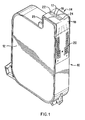
- Fig. 1 is a perspective view of an inkjet print cartridge according to one embodiment of the present invention.
- Fig. 2 is a facial (unfolded flat) view of the front surface of the Tape Automated Bonding (TAB) printhead assembly ("THA”) removed from the print cartridge of Fig. 1.
- TAB Tape Automated Bonding
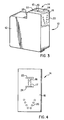
- Fig. 3 is a perspective view of a simplified, schematic form of the inkjet print cartridge of Fig. 1. for illustrative purposes.
- Fig. 4 is a facial (unfolded flat) view of the front surface of the Tape Automated Bonding (TAB) printhead assembly (hereinafter “TAB head assembly”) removed from the print cartridge of Fig. 3.
- TAB Tape Automated Bonding
- Fig. 5 is a perspective view of the back surface of the TAB head assembly of Fig. 4 with a silicon substrate mounted thereon and the conductive leads attached to the substrate.
- Fig. 6 is a side elevational view in cross-section taken along line A-A in Fig. 5 illustrating one system (compare the above-mentioned application 08/558,567 for a more highly preferred system) for attachment of conductive leads to electrodes on the silicon substrate.
- Fig. 7 is a top perspective view of a substrate structure containing heater resistors, ink channels, and vaporization chambers, which is mounted on the back of the TAB head assembly of Fig. 4.
- Fig. 8 illustrates one process which may be used to form the preferred TAB head assembly.
- Fig. 9 is a schematic diagram for a fiber push connect laser system as used in the present invention.
- Fig. 10 shows in detail-butvery schematically-theflex circuit, a spot weld point, the TAB lead and the die pad for embodiments in which the thickness of gold on the die is considerably smaller than a barrier layer which may be present, underlying the gold (used to form, for instance, inkjet chambers and channels).
- Fig. 10A analogously shows in detail the same features for embodiments in which the thickness of gold is equal to the barrier-layer height.
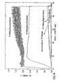
- Fig. 11 shows the temperature profile of the flex circuit, weld beam and spot weld location as measured during a related laser-welding process for interbonding leads (traces) of the die and substrate-with the FPC laser, but using adhesive for mechanical connection of the TAB tape and the substrate.
- Fig. 12 shows the absorption property versus wavelength for various metals.
- Fig. 13 illustrates the optical transmission results for five samples of Kapton® tape sputtered with 2, 5, 10, 15, and 25 nm of chromium.
- Fig. 14 illustrates the temperature rise in flex circuits with Ti/W seed layers.
- Fig. 15 illustrates the temperature rise in flex circuits with a chromium seed layer.
- Fig. 16 illustrates temperature increase versus time in a 3-layer tape with different thickness chromium seed layers.
- Fig. 17 illustrates a first embodiment of the present invention.
- Fig. 18 illustrates a variation of the Fig. 17 embodiment.
- Fig. 19 illustrates a second embodiment of the present invention.
- Fig. 20 illustrates a third embodiment of the present invention.
- Fig. 21 illustrates a variation of the Fig. 20 embodiment.
- Fig. 22 illustrates a fourth embodiment of the present invention.
- the present method and apparatus for the solderless laser welding of two materials by using a laser light beam attached to a fiber optic system is applicable to laser welding of other types of electrical members to each other.
- reference numeral 10 generally indicates an inkjet print cartridge incorporating a printhead according to one embodiment of the present invention simplified for illustrative purposes.
- the inkjet print cartridge 10 includes an ink reservoir 12 and a printhead 14, where the printhead 14 is formed using Tape Automated Bonding (TAB).
- TAB head assembly 14 includes a nozzle member 16 comprising two parallel columns of offset holes or orifices 17 formed in a flexible polymer flexible circuit 18 by, for example, laser ablation.
- a back surface of the flexible circuit 18 includes conductive traces 36 formed thereon using a conventional photolithographic etching and/or plating process. These conductive traces 36 are terminated by large contact pads 20 designed to interconnect with a printer.
- the print cartridge 10 is designed to be installed in a printer so that the contact pads 20, on the front surface of the flexible circuit 18, contact printer electrodes providing externally generated energization signals to the printhead. Bonding areas 22 and 24 in the flexible circuit 18 are where the bonding of the conductive traces 36 to electrodes on a silicon substrate containing heater resistors occurs.
- the flexible circuit 18 is bent over the back edge of the print cartridge "snout" and extends approximately one half the length of the back wall 25 of the snout. This flap portion of the flexible circuit 18 is needed for the routing of conductive traces 36 which are connected to the substrate electrodes, most particularly those which are connected through the far end window 22.
- the contact pads 20 are located on the flexible circuit 18 which is secured to this wall and the conductive traces 36 are routed over the bend and are connected to the substrate electrodes through the windows 22, 24 in the flexible circuit 18.
- Fig. 2 shows a face view of the TAB head assembly 14 of Fig. 1 while still flat and before attachment to the print cartridge 10 and prior to windows 22 and 24 in the TAB head assembly 14 being filled with an encapsulant.
- TAB head assembly 14 has affixed to the back of the flexible circuit 18 a silicon substrate 28 (not shown) containing a plurality of individually energizable thin film resistors. Each resistor is located generally behind a single orifice 17 and acts as an ohmic heater when selectively energized by one or more pulses applied sequentially or simultaneously to one or more of the contact pads 20.
- the orifices 17 and conductive traces 36 may be of any size, depth or thickness respectively, and pattern, and the various figures are designed to simply and clearly show the features of the invention. The relative dimensions of the various features have been greatly adjusted for the sake of clarity.
- the orifice 17 pattern on the flexible circuit 18 shown in Fig. 2 may be formed by a masking process in combination with a laser or other etching means in a step-and-repeat process, which would be readily understood by one of ordinary skill in the art after reading this disclosure.
- Fig. 14, to be described in detail later, provides additional details of this process. Further details regarding TAB head assembly 14 and flexible circuit 18 are provided below.
- Fig. 3 is a perspective view of a schematic form of the inkjet print cartridge of Fig. 1, simplified for illustrative purposes.
- Fig. 4 is a view of the front surface of the Tape Automated Bonding (TAB) printhead assembly (hereinafter “TAB head assembly”) shown flat and before attachment to the simplified print cartridge of Fig. 3.
- TAB Tape Automated Bonding
- Fig. 5 shows the back surface of the TAB head assembly 14 of Fig. 4 showing the silicon die or substrate 28 mounted to the back of the flexible circuit 18 and also showing one edge of the barrier layer 30 formed on the substrate 28 containing ink channels and vaporization chambers.
- Fig. 7 shows greater detail of this barrier layer 30 and will be discussed later. Shown along the edge of the barrier layer 30 are the entrances to the ink channels 32 which receive ink from the ink reservoir 12.
- the conductive traces 36 formed on the back of the flexible circuit 18 terminate in contact pads 20 ( shown in Fig. 4) on the opposite side of the flexible circuit 18 at location 38.
- the bonding areas 22 and 24 locate where the conductive traces 36 and the substrate electrodes 40 (shown in Fig. 6) are bonded by using a laser light beam attached to a fiber optic system which directs the light to the location to be bonded in accordance with the present invention.
- Fig. 6 shows a side view cross-section taken along line A-A in Fig. 5 illustrating the connection of the ends of the conductive traces 36 to the electrodes 40 formed on the substrate 28.
- a portion 42 of the barrier layer 30 is used to insulate the ends of the conductive traces 36 from the substrate 28.
- Fig. 6 is a side view of the flexible circuit 18, the barrier layer 30, the bonding areas 22 and 24, and the entrances of the various ink channels 32. Droplets of ink 46 are shown being ejected from orifice holes associated with each of the ink channels 32.
- Fig. 7 is a front perspective view of the silicon substrate 28 which is affixed to the back of the flexible circuit 18 in Fig. 5 to form the TAB head assembly 14. Silicon substrate 28 has formed on it, using conventional photolithographic techniques, two rows or columns of thin film resistors 70, shown in Fig. 7 exposed through the vaporization chambers 72 formed in the barrier layer 30.
- the substrate 28 is approximately one-half inch long and contains 300 heater resistors 70, thus enabling a resolution of 600 dots per inch.
- Heater resistors 70 may instead be any other type of ink ejection element, such as a piezoelectric pump-type element or any other conventional element.
- element 70 in all the various figures may be considered to be piezoelectric elements in an alternative embodiment without invalidating the herein-relevant general principles of hydrodynamic operation of the printhead.
- electrodes 74 for connection to the conductive traces 36 (shown by dashed lines) formed on the back of the flexible circuit 18.
- a demultiplexer 78 shown by a dashed outline in Fig. 7, is also formed on the substrate 28 for demultiplexing the incoming multiplexed signals applied to the electrodes 74 and distributing the signals to the various thin film resistors 70.
- the demultiplexer 78 enables the use of many fewer electrodes 74 than thin film resistors 70. Having fewer electrodes allows all connections to the substrate to be made from the short end portions of the substrate, so that these connections will not interfere with the ink flow around the long sides of the substrate.
- the demultiplexer 78 may be any decoder for decoding encoded signals applied to the electrodes 74.
- the demultiplexer has input leads (omitted for simplicity) connected to the electrodes 74 and has output leads (not shown) connected to the various resistors 70.
- the demultiplexer 78 circuity is discussed in further detail below.
- barrier layer 30 which may be a layer of photoresist or some other polymer, in which is formed the vaporization chambers 72 and ink channels 80.
- a portion 42 of the barrier layer 30 insulates the conductive traces 36 from the underlying substrate 28, as previously discussed with respect to Fig. 4.
- the substrate structure is positioned with respect to the back surface of the flexible circuit 18 so as to align the resistors 70 with the orifices formed in the flexible circuit 18.
- This alignment step also inherently aligns the electrodes 74 with the ends of the conductive traces 36.
- the top surface of the barrier layer 30 is then bonded to the back surface of the flexible circuit 18.
- the traces 36 are then bonded to the electrodes 74.
- Fig. 8 illustrates one method for forming the TAB head assembly 14.
- the starting material is a Kapton® or Upilex® type polymer tape 104, although the tape 104 can be any suitable polymer film which is acceptable for use in the below-described procedure. Some such films may comprise teflon, polyamide or polyimide, polymethylmethacrylate, polycarbonate, polyester, polyamide or polyimide polyethylene-terephthalate or mixtures thereof.
- the tape 104 is typically provided in long strips on a reel 105.
- Sprocket holes 106 along the sides of the tape 104 are used to accurately and securely transport the tape 104.
- the sprocket holes 106 may be omitted and the tape may be transported with other types of fixtures.
- the tape 104 is already provided with conductive copper traces 36, such as shown in Figs. 2, 4 and 5, formed thereon using conventional metal deposition and photolithographic processes.
- conductive copper traces 36 such as shown in Figs. 2, 4 and 5, formed thereon using conventional metal deposition and photolithographic processes.
- the particular pattern of conductive traces depends on the manner in which it is desired to distribute electrical signals to the electrodes formed on silicon dies, which are subsequently mounted on the tape 104.
- the tape 104 is transported to a laser processing chamber and laser-ablated in a pattern defined by one or more masks 108 using laser radiation 110, such as that generated by an Excimer laser 112.
- laser radiation 110 such as that generated by an Excimer laser 112.
- the masked laser radiation is designated by arrows 114.
- such masks 108 define all of the ablated features for an extended area of the tape 104, for example encompassing multiple orifices in the case of an orifice pattern mask 108, and multiple vaporization chambers in the case of a vaporization chamber pattern mask 108.
- the laser system for this process generally includes beam delivery optics, alignment optics, a high precision and high speed mask shuttle system, and a processing chamber including a mechanism for handling and positioning the tape 104.
- the laser system uses a projection mask configuration wherein a precision lens 115 interposed between the mask 108 and the tape 104 projects the Excimer laser light onto the tape 104 in the image of the pattern defined on the mask 108.
- the masked laser radiation exiting from lens 115 is represented by arrows 116.
- Such a projection mask configuration is advantageous for high precision orifice dimensions, because the mask can be physically remote from the nozzle member.
- a next step in the process is a cleaning step wherein the laser ablated portion of the tape 104 is positioned under a cleaning station 117. At the cleaning station 117, debris from the laser ablation is removed according to standard industry practice.
- the tape 104 is then stepped to the next station, which is an optical alignment station 118 incorporated in a conventional automatic TAB bonder, such as an inner lead bonder commercially available from Shinkawa Corporation, Model No. ILT-75.
- the bonder is preprogrammed with an alignment (target) pattern on the nozzle member, created in the same manner and/or step as used to create the orifices, and a target pattern on the substrate, created in the same manner and/or step used to create the resistors.
- the nozzle member material is semitransparent so that the target pattern on the substrate may be viewed through the nozzle member.
- the bonder then automatically positions the silicon dies 120 with respect to the nozzle members so as to align the two target patterns.
- the alignment of the silicon dies 120 with respect to the tape 104 is performed automatically using only commercially available equipment.
- By integrating the conductive traces with the nozzle member, such an alignment feature is possible.
- Such integration not only reduces the assembly cost of the printhead but reduces the printhead material cost as well.
- the automatic TAB bonder then uses a gang bonding method to bond the conductive traces down onto the associated substrate electrodes as described in U.S. Patent Application Serial No. 08/558,567, filed October 31, 1995, entitled Solderless Connection of Electrical Contacts Utilizing Combination Laser and Fiber Optic Push Connect System; which is herein incorporated by reference.
- the tape 104 is then stepped to station 122 to affix the top surface of the barrier layer 30 to the back surface of the flexible circuit 18.
- higher bond temperatures are generally preferred to decrease the bond time, but higher bond temperatures will soften the flex circuit and cause more deformation of the Kapton tape.
- higher temperature at the contact point and lower temperature at the Kapton tape layer may be achieved by utilizing a Fiber Push Connect (FPC) single point laser welding process.
- FPC in conjunction with a TAB circuit provides an ideal solution for a TAB head assembly for an inkjet printer printhead.
- FIG. 9 A schematic for a FPC laser system 200 is illustrated in Fig. 9.
- This system consists of an Nd YAG or diode laser 202, equipped with a glass (SiO 2 ) optical fiber 204.
- the system guides the laser beam to the contact or attachment point 206 via the optical glass fiber 204.
- An optimum thermal coupling is achieved by pressing two parts together by means of the fiber 204 which creates a zero contact gap between the TAB gold bond line 210 and die gold bond line 208 and thus improved thermal efficiency.
- Figs. 10 and 10A show in greater detail but very schematically the flex circuit 18, the contact region 206, the TAB gold bond line 210 and die gold bond line 208-intwo variants relating to the specific configuration of the gold 208 on the die or substrate 28.
- a feedback temperature loop is achieved by means of an infrared detector 212 through the glass fiber.
- the temperature or absorption behavior response of the IR-radiation reflected by the gold bond lines 208, 210 at the contact point 206 is gathered.
- the outgoing laser beam 220 from the laser source 202 goes through a half-transmission mirror or beam splitter 214 and through a focussing lens 216 into the glass fiber optic 204.
- the reflected light 218 from the fiber optic shown with dashed lines is reflected by the half mirror 21 and arrives via focussing lens 222 at an IR detector 212 that is connected to a PC Controller 224.
- the graph shown on the monitor 226 of PC controller 224 is meant to show that the PC Controller 224 can store definite expected plots for the temperature variation of the laser welding process with which the actual temperature variation can be compared.
- the PC Controller 224 is connected with the laser source 202 so that the laser parameters can be controlled if necessary.
- the reproducibility of an FPC laser bond depends both on a high degree of thermal coupling between the gold bond lines 208, 210 and high absorption of the laser energy by those bond lines 208, 210.
- minimum absorption is desired in the Kapton tape and maximum absorption is desired in the gold bond lines 208, 210.
- Metals with higher absorption rate will transform a higher share of the laser energy into heat. This will result in a shorter attachment process which in turn will result in a higher-quality bond.
- the laser utilized is a YAG laser with a wavelength of 1064 nm.
- Fig. 12 illustrates the absorption property versus wavelength for several metals.
- Chromium was selected as the base metal due to the fact that most flex circuit manufacturers are using chromium as the seed layer.
- the penetration depth of the laser into chromium is about 10 nm with a spot size of 5 nm; this requires a minimum chromium thickness of 15 nm.
- the laser beam creates a localized heated zone causing the metals (or solder material), to melt and create a bond between two joining surfaces without increasing the temperature of the Kapton tape. However, any gap between two mating metal parts will cause overheating of the metal surface exposed to the laser beam. This will cause deformation of the flexible circuit 18 with no bond between metal surfaces. Also, an increased temperature in the flex circuit 18 will cause damage to the flex circuit.
- Fig. 11 illustrates a typical temperature profile of the flex circuit 18, measured during a laser lead-bonding process with the FPC laser. (The thermal environment in that process is closely related to that of the present invention; however, for the mechanical connection between die and tape it uses adhesive rather than welding.) As can be observed from Fig. 11, the temperature at the attachment region 206 is considerably higher than the Kapton tape 18 temperature. This is achieved due to the high degree of transparency of the Kapton tape at different wavelengths.
- the Kapton polyimide tape is transparent to the YAG laser beam and the laser beam passes through the 2 mil thick layer of polyimide with minimal absorption.
- Chromium is a conventional seed layer that is used extensively to provide an adhesion layer between the copper trace and Kapton polyimide in a two-layer flex circuit manufacturing process.
- a chromium layer with a minimum thickness of 10 nm (or 20 nm nominal) is required to provide a medium which absorbs the laser energy.
- the thickness of the chromium layer varies depending upon the flex circuit manufacturer, with reported thicknesses between 2 and 30 nm.
- a typical flex circuit manufacturing process utilizes a thin layer (20 nm) of sputtered chromium as a seed (adhesion) layer between the copper traces and Kapton polyimide.
- Figure 13 illustrates the optical transmission results for these samples. It can be seen that optical transmission initially drops rapidly with increased chromium thickness (from 65% for 2 nm of chromium, to 12% for 15 nm of chromium), but optical transmission changes very slowly when chromium thickness increases from 15 to 25 nm.
- Figs. 14 and 15 illustrate temperature rise in several flex circuits with different constructions.
- Fig. 14 illustrates temperature rise in flex circuits with thicker seed layers. It is important to notice that flex circuits with 10 nm or less of Ti/W did not reach the temperature that is required for gold/gold laser welding, but the flex circuit with 20 nm of Ti/W did reach the laser welding temperature. Also, it should be noted that the rise time in the flex circuit with thicker Ti/W is faster, minimizing the potential of damage due to high localized temperatures in the Kapton tape.
- the temperature (IR-Signal) fluctuation in the flex circuit with 20 nm of Ti/W is indicative of the fact that this flex circuit reached the maximum preset temperature required for gold/gold laser welding and then the laser feed-back loop temporarily dropped the laser energy so that increase in the TAB bond temperature did not damage the Kapton tape. As soon as the temperature of the Kapton tape dropped (by a preset amount), the laser energy automatically increased to full power to increase the TAB gold bond line temperature, and created a reliable gold/gold bond.
- Fig. 15 illustrates similar results for different flex circuits with a chromium seed layer as opposed to Ti/W seed layer. It can be observed that a flex circuit with 10 nm of chromium did reach the preset temperature required for gold/gold welding. Therefore, chromium seed layer has higher absorption characteristics compared to Ti/W seed layer for a YAG laser.
- Fig. 16 illustrates temperature increase versus time in a 3-layer tape with a 20 nm chromium layer, a tape with a 5 nm chromium layer, and a tape with no chromium layer. As can be seen in Fig. 16, only the flex circuit with a 20 nm chromium layer indicated a rapid temperature rise.
- chromium thickness is essential to the integrity of the gold/gold laser bond
- an optimum chromium thickness was selected as a base line. Referring to Fig. 13, a chromium thickness over 15 nm does not decrease transmission importantly. Based on Fig. 15, a chromium thickness of 10 nanometers is the absolute minimum required thickness to provide a successful laser bond. Fig. 15 also illustrates that a flex circuit with 15 nm of chromium exhibits a much faster temperature rise in the copper trace, resulting in less or no damage to the Kapton tape. Therefore, 15 nm of chromium is optimum to provide a reliable and repeatable laser bond.
- Some chromium diffusion into the copper is expected during the sputtering of chromium as a seed layer and plating processes during manufacture of the flex circuits. Diffusion of the chromium into the copper is a time and temperature dependent process, and it is difficult to determine the amount of chromium that will be diffused into the copper during these processes. Normally, it is estimated that a maximum amount of diffused chromium is under 5 nm. Based on these factors, a minimum chromium thickness after the sputtering process was established as 20 nm. This thickness should guarantee a minimum chromium thickness of 15 nm after the completed manufacture of the flex circuit.
- Figs. 17 to 22 show various embodiments of the present invention.
- view (A) shows the gold layer 208 on the substrate, and the substrate barrier structure 30 as such (where visible) including ink vaporization chambers 72 and chamber walls 71, 73, and also shows firing resistors 70;
- view (B) shows a cross-section taken along line B-B of view (A);
- view (C) shows the weld seam pattern 210 on the underside of the Kapton tape (but viewed from above, as if through the tape), and also the nozzle apertures 17.
- the walls 71, 73 of the vaporization chamber 72 are laid down in gold 208 on the substrate or die 28.
- the conventional material of the barrier layer 30 is completely replaced with gold to construct the ink ejection chambers 72-orin other words the barrier layer 30 is itself identically the gold layer 208 (as suggested by the notation 30, 208 in the drawing).
- the gold thickness 208' is of the order of 15 ⁇ m, with the exact value depending on the printhead architecture, and this configuration may be regarded as corresponding very generally to the highly schematic showing in Fig. 10.
- the outline of the side walls 71 and rear wall 73 of the vaporization chamber 72 forms a gold weld line pattern on the barrier layer 30.
- a corresponding mating gold weld line pattern 210 (only a relatively narrow line, in comparison with the width of the gold 208 on the substrate) is laid on underside of the flex circuit to match that outline of the vaporization chambers 72. More specifically this weld seam 210 is made of copper laid on a chromium seed layer and coated with gold to prevent corrosion.
- the substrate 30 and flex circuit 18 are precisely aligned and welded using the FPC laser welding system and technique as described above. The position of the FPC probe is moved along the weld seam, to create a weld line, by using overlapping patterns of spot welds.
- the advantages of this embodiment are resistance to corrosion and delamination resulting in better reliability and better stiffness, resulting in better dot placement and refill performances, thereby resulting in better print quality.
- FIG. 18 A modified form of this embodiment is shown in Fig. 18.
- a weld seam pattern 210 is laid on the underside of the flex circuit 18 to match the outline of the vaporization chamber 72.
- This weld seam 210 is made of copper laid on a chromium seed layer and coated with gold to prevent corrosion.
- the substrate 28 and the flex 18 are precisely aligned and welded using the FPC welding system. The position of the FPC probe is moved along the weld seam, to create a weld line, by using overlapping patterns of spot welds.
- the main advantage of this embodiment is better stiffness, resulting in better dot placement and refill performances, thereby resulting in better print quality. Since the thickness 208' of gold 208 is considerably smaller than that 30' of the conventional barrier material 30, this configuration too may be regarded as very generally corresponding to the highly schematic showing of Fig. 10.
- the walls 71, 73 of the vaporization chambers 72 are again laid down entirely in gold 208 on the substrate or die 28, very generally as in Fig. 17-and so here too corresponding very generally to the schematic showing in Fig. 10.
- the height/thickness 208' of the vaporization chamber 72 on the substrate is on the order of only 1 to 2 ⁇ m.
- This embodiment is advantageous if plating up to the wall 71 height thicknesses of approximately 15 microns is difficult for the manufacturing process to handle.
- the outline of the vaporization-chamber walls 71, 73 laid out in gold 208 on the surface of the barrier layer 30 forms a gold weld line pattern.
- the remainder of the vaporization chamber 72 is formed by ablating a recess in the underside of the flex 18 to match that ink-chamber layout of the gold barrier.
- a corresponding mating gold weld seam pattern 210 is laid on the underside of the flex circuit 18.
- This weld seam is made of copper laid on a chromium seed layer and coated with gold to prevent corrosion.
- the substrate 30 and the flex 18 are precisely aligned and welded using the FPC welding system. The position of the FPC probe is moved along the weld seam, to create a weld line, by using overlapping patterns of spot welds.
- the advantages of this embodiment are resistance to corrosion and delamination resulting in better reliability, better stiffness, resulting in better dot placement and refill performances, thereby resulting in better print quality.
- the side walls 71 of the vaporization chambers 72 are again made of the conventional barrier material 30 but the critical back wall 73, formed with a straight edge including segments that extend across the lands or peninsulas 30 between the individual chambers 72, is fabricated completely out of gold 208.
- both gold 208 and conventional barrier material 30 are present side by side, and the respective heights/thicknesses 208', 30' of the gold 208 and of the conventional barrier material 30 are substantially the same, as seen in the (C) view, and this configuration may be regarded as corresponding very generally to the highly schematic variant showing of Fig. 10A.
- a corresponding mating gold weld seam pattern here taking the form of a simple straight line 210, is laid on the underside of the flex circuit 18 to match the outline of the vaporization chamber back wall 73.
- This weld seam is made of copper laid on a chromium seed layer and coated with gold to prevent corrosion.
- the substrate 30 and flex circuit 18 are precisely aligned and welded using the FPC laser welding system. The position of the FPC probe is moved along the seam, to create a weld line, by using overlapping patterns of spot welds.
- the advantages of this embodiment are resistance to corrosion and delamination-resulting in better reliability and stiffness, resulting in better dot placement and refill performances, thereby resulting in better print quality.
- a variation of this embodiment, shown in Fig. 21, is to build only the top 1 to 2 ⁇ m thickness 208' of the back wall 73 barrier structure with gold 208, its underlayment being a thickness 30' of conventional barrier material 30.
- a straight-line weld seam pattern 210 is laid on the underside of the flex circuit 18 to match the rectilinear outline of the vaporization-chamber back wall 73.
- This weld seam is made of copper laid on a chromium seed layer and coated with gold to prevent corrosion.
- the substrate and the flex are precisely aligned and welded using the FPC welding system.
- the position of the FPC probe is moved along the weld seam, to create a weld line, by using overlapping patterns of spot welds.
- the main advantage of this embodiment is better stiffness, resulting in better dot placement and refill performances, thereby resulting in better print quality.
- This configuration too, since the gold 208 is very thin relative to the conventional barrier material 30, may be seen as
- the entire vaporization chamber 72 is built of conventional barrier material 30, but a straight gold baffle bar 77 is formed along (as shown) or slightly behind the back walls 73 of the vaporization chambers 72 to form a gold weld line pattern 210.
- This configuration accordingly may be seen as corresponding to Fig. 10A.
- this baffle structure 77 is preferably built slightly behind the back wall 73, essentially in a slot or trench provided in the conventional barrier material.
- the baffle structure 77 can be fabricated either by placing a thin 1-2 ⁇ m gold weld seam pattern 210 on the substrate 30 and a thick (same thickness as the vaporization chamber 72) weld trace on the underside of the flex 18 or by laying a thick gold structure (same thickness 208', 30' as the vaporization-chamber walls 72) on the substrate 30 and a 1-2 ⁇ m weld seam line 210 on the flex 18.
- the thickness in traces can also be shared between the substrate 30 and the flex 18 to meet specific design rules for the product and process.
- the main advantage of this embodiment is better stiffness, resulting in better dot placement and refill performances, thereby resulting in better print quality.
- the FPC laser is used to form a full weld along the gold weld lines or weld patterns 208, 210.
- Experimental results show that average peel strengths using FPC laser welding are roughly 80 newtons (18.3 lbs.) versus 15 newtons (3.6 lbs.) for conventional adhesive bonding. Accordingly, with due allowance for variations, the methods of the present invention are deemed to encompass providing peel strengths exceeding about 20 newtons (approximately 41 ⁇ 2 pounds force) and preferably exceeding about 60 newtons (approximately 131 ⁇ 2 pounds force).
- the tape 104 steps forward and is optionally taken up on the take-up reel 124.
- the tape 104 may then later be cut to separate the individual TAB head assemblies from one another.
- the resulting TAB head assembly is then positioned on the print cartridge 10, and the previously described adhesive seal 90 is formed to firmly secure the nozzle member to the print cartridge, provide an ink-proof seal around the substrate between the nozzle member and the ink reservoir, and encapsulate the traces in the vicinity of the headland so as to isolate the traces from the ink.
- Peripheral points on the flexible TAB head assembly are then secured to the plastic print cartridge 10 by a conventional melt-through type bonding process to cause the polymer flexible circuit 18 to remain relatively flush with the surface of the print cartridge 10, as shown in Fig. 1.
- the present invention was described in conjunction with the laser welding of a TAB circuit to the silicon substrate of an inkjet printhead, the present method and apparatus for the solderless laser welding of two materials by using a laser light beam attached to a fiber optic system is applicable to laser welding of other types of materials to each other.
- the present invention was described in conjunction with solderless gold-to-gold laser welding of two materials to each other, the present method could be used for the solderless laser welding using other conductive metals.
Landscapes
- Engineering & Computer Science (AREA)
- Manufacturing & Machinery (AREA)
- Physics & Mathematics (AREA)
- Optics & Photonics (AREA)
- Particle Formation And Scattering Control In Inkjet Printers (AREA)
- Lining Or Joining Of Plastics Or The Like (AREA)
- Laser Beam Processing (AREA)
Abstract
Description
The invention improves the quality, repeatability and reliability of the pen and results in less process steps, thereby improving processing time, cost and reduced in-process handling.
Claims (15)
- A method of mechanical connection of two nonmetallic materials (18, 28) by laser welding using a laser beam (220) having a specified wavelength; said method being substantially distinct from formation of functional plural electrical connections (40, 36), and comprising the steps of:providing a first nonmetallic material (28) with a first weldable-metal pattern (208) thereon or therein;providing a second nonmetallic material (18) with a seed-metal pattern (210) thereon or therein, and a second weldable-metal pattern (210) on the seed-metal pattern, said seed metal having a suitable absorption at the specified wavelength of the laser beam;wherein optionally at least one of the weldable-metal patterns is not for conduction of electricity after welding is complete; andlaser welding (Fig. 9) the metal patterns together.
- The method of claim 1, as used for fastening of a tape, such as for example a TAB circuit (Fig. 2), to another article; and wherein:the second-mentioned providing step comprises providing the seed-metal and second weldable-metal patterns on or in the tape; andpreferably the laser welding step comprises laser welding the weldable-metal patterns together by directing a laser beam (220) to heat the seed-metal pattern.
- The method of claim 2, for use with said second article that comprises a silicon substrate, and wherein:said first-mentioned pattern providing step comprises providing a weldable-metal pattern on or in the silicon substrate.
- The method of claim 2, for use with said second article that comprises a substrate (28) which includes a barrier layer (30) having an upstanding barrier-layer pattern to define a contoured structure, such as chambers (72) and channels (80); and wherein:the first-pattern providing step comprises forming the first pattern (Figs. 17-22[C]) on or in the substrate in accordance with at least a portion of the barrier-layer pattern (Figs. 17-22[A]).
- The method of claim 4, wherein:the first-pattern providing step comprises at least one step selected from the group consisting of:substantially applying the first weldable metal to the top (Fig. 18[B]) of the barrier layer;substantially applying the first weldable metal to the substrate (Fig. 19[B]), to form at least the chambers and channels of the barrier layer, and preferably also forming a structure of cavities in material of the tape, aligned with the chambers
and channels of the barrier layer, to effectively enlarge the chambers and channels;substantially applying the first weldable metal to form a structure (Fig. 20-22[C]) that is generally aligned with a major feature of the barrier-layer pattern; said aligned structure preferably including a bulkhead (77) that is behind and extends generally parallel to rear walls (73) of chambers of the barrier layer; andsubstantially applying the first weldable metal to form a structure (77) that generally reenforces a major feature (73) of the barrier-layer pattern. - The method of claim 5, wherein:the preferable cavity-structure forming step, if present, comprises laser ablation of the tape.
- The method of any one of claims 4 through 6, for forming an inkjet-printhead assembly (Figs. 1, 3) that includes a TAB circuit (Figs. 2, 4) and a substrate, and wherein:the tape comprises a TAB circuit;said second article comprises a substrate of an inkjet printhead (Figs. 1, 3); andsaid chambers and channels are for holding ink (46).
- The method of any one of claims 4 through 7, wherein:peel strength as between the tape and the substrate exceeds 20 newtons (approximately 4½ pounds force), and preferably exceeds 60 newtons (approximately 13½ pounds force).
- The method of any one of claims 1 through 7, wherein:although substantially distinct from formation of functional plural electrical connections, performance of at least some of the steps of the method is simultaneous or substantially concurrent with steps in formation of functional electrical connections between conductors (36, 40) on the two nonmetallic materials.
- The method of any one of claims 1 through 7:further comprising using an optical fiber (204) to hold the weldable-metal
patterns in contact at a bond surface (208/210); andwherein the laser-welding step comprises directing the laser beam through the optical fiber; andpreferably further comprising the step of, before the welding step, substantially aligning the weldable-metal
patterns on the surfaces of the first and second materials respectively. - The method of any one of claims 1 through 7, wherein:the directing step comprises directing the laser beam to the seed-metal pattern through bulk substance of the second nonmetallic material.
- The method of any one of claims 1 through 7, wherein:the specific wavelength (YAG) of the laser beam is in the near infrared; andthe second providing step comprises using chromium to form the seed-metal pattern; andpreferably the laser welding step comprises using an yttrium-aluminum-garnet laser to form the laser beam.
- The method of claim 11, wherein:the second providing step provides a seed-metal pattern at least ten nanometers thick.
- The method of any one of claims 1 through 7, wherein:the two material-providing steps both provide substantially identical weldable metals;whereby the laser beam literally welds two layers of a common metal, as distinguished from soldering; andpreferably the two material-providing steps both provide patterns of gold.
- An assembly (Fig. 5; Fig. 1) made by the method of any one of claims 1 through 14.
Applications Claiming Priority (2)
| Application Number | Priority Date | Filing Date | Title |
|---|---|---|---|
| US08/705,928 US5847356A (en) | 1996-08-30 | 1996-08-30 | Laser welded inkjet printhead assembly utilizing a combination laser and fiber optic push connect system |
| US705928 | 1996-08-30 |
Publications (3)
| Publication Number | Publication Date |
|---|---|
| EP0826503A2 true EP0826503A2 (en) | 1998-03-04 |
| EP0826503A3 EP0826503A3 (en) | 1999-01-27 |
| EP0826503B1 EP0826503B1 (en) | 2002-08-14 |
Family
ID=24835510
Family Applications (1)
| Application Number | Title | Priority Date | Filing Date |
|---|---|---|---|
| EP97306725A Expired - Lifetime EP0826503B1 (en) | 1996-08-30 | 1997-09-01 | Laser welding nonmetallic assemblies, such as T.A.B. tapes to semiconductor elements, particularly inkjet printheads |
Country Status (4)
| Country | Link |
|---|---|
| US (2) | US5847356A (en) |
| EP (1) | EP0826503B1 (en) |
| JP (1) | JP4081160B2 (en) |
| DE (1) | DE69714670T2 (en) |
Cited By (1)
| Publication number | Priority date | Publication date | Assignee | Title |
|---|---|---|---|---|
| WO2006000273A1 (en) | 2004-06-24 | 2006-01-05 | Forschungszentrum Karlsruhe Gmbh | Method for joining plastic workpieces |
Families Citing this family (34)
| Publication number | Priority date | Publication date | Assignee | Title |
|---|---|---|---|---|
| DE19504967C2 (en) | 1995-02-15 | 2002-01-24 | Fraunhofer Ges Forschung | Method for connecting a flexible substrate to a chip |
| US6236015B1 (en) | 1995-10-31 | 2001-05-22 | Hewlett-Packard Company | Method for predicting and avoiding a bad bond when utilizing fiber push connect laser bonding |
| US5847356A (en) * | 1996-08-30 | 1998-12-08 | Hewlett-Packard Company | Laser welded inkjet printhead assembly utilizing a combination laser and fiber optic push connect system |
| FR2763746B1 (en) * | 1997-05-23 | 1999-07-30 | Thomson Csf | METHOD AND DEVICE FOR CONNECTING TWO MILLIMETER ELEMENTS |
| AUPP653998A0 (en) * | 1998-10-16 | 1998-11-05 | Silverbrook Research Pty Ltd | Micromechanical device and method (ij46B) |
| AUPP653598A0 (en) * | 1998-10-16 | 1998-11-05 | Silverbrook Research Pty Ltd | Micromechanical device and method (ij46C) |
| DE19751487A1 (en) * | 1997-11-20 | 1999-06-02 | Pac Tech Gmbh | Method and device for the thermal connection of pads of two substrates |
| AU1139100A (en) | 1998-10-16 | 2000-05-08 | Silverbrook Research Pty Limited | Improvements relating to inkjet printers |
| US7216956B2 (en) * | 1998-10-16 | 2007-05-15 | Silverbrook Research Pty Ltd | Printhead assembly with power and ground connections along single edge |
| JP3560135B2 (en) * | 1999-03-23 | 2004-09-02 | 日産自動車株式会社 | Quality monitoring method for YAG laser welds |
| AU2001247240A1 (en) * | 2000-03-01 | 2001-09-12 | Heraeus Amersil, Inc. | Method, apparatus, and article of manufacture for determining an amount of energy needed to bring a quartz workpiece to a fusion weldable condition |
| US6619786B2 (en) | 2001-06-08 | 2003-09-16 | Lexmark International, Inc. | Tab circuit for ink jet printer cartridges |
| US20040135988A1 (en) * | 2001-09-24 | 2004-07-15 | Robert Link | Method and device for producing an intermediate supporting strip by welding and involving a subsequent heat treatment |
| CN1222929C (en) * | 2001-10-11 | 2005-10-12 | 新科实业有限公司 | SBB machine and method for HGA mass production |
| US20030071269A1 (en) * | 2001-10-15 | 2003-04-17 | Tseng Ampere A. | Apparatus and method for laser selective bonding technique for making sealed or enclosed microchannel structures |
| DE60333364D1 (en) * | 2002-05-24 | 2010-08-26 | Koninkl Philips Electronics Nv | METHOD FOR TRANSMITTING A BUILDING ELEMENT ATTACHED TO A CARRIER INTO A DESIRED POSITION ON A CARRIER AND DEVICE THEREFOR |
| US6811250B2 (en) * | 2002-11-19 | 2004-11-02 | Lexmark International, Inc. | Ink conduit plugs for an inkjet printhead and methods of laser welding same |
| US20040150688A1 (en) * | 2003-01-30 | 2004-08-05 | Kin-Ming Kwan | Measuring laser light transmissivity in a to-be-welded region of a work piece |
| US20040257412A1 (en) * | 2003-06-18 | 2004-12-23 | Anderson James D. | Sealed fluidic interfaces for an ink source regulator for an inkjet printer |
| US20050099449A1 (en) * | 2003-11-07 | 2005-05-12 | Tim Frasure | Methods and structures for disassembling inkjet printhead components and control therefor |
| JP4553348B2 (en) * | 2003-12-03 | 2010-09-29 | キヤノン株式会社 | Inkjet recording head |
| US7404613B2 (en) * | 2004-06-30 | 2008-07-29 | Lexmark International, Inc. | Inkjet print cartridge having an adhesive with improved dimensional control |
| US7820936B2 (en) * | 2004-07-02 | 2010-10-26 | Boston Scientific Scimed, Inc. | Method and apparatus for controlling and adjusting the intensity profile of a laser beam employed in a laser welder for welding polymeric and metallic components |
| CN100496749C (en) * | 2004-07-06 | 2009-06-10 | 犹他大学研究基金会 | Spotting device and method for high concentration spot deposition on microarrays and other microdevices |
| US7291226B2 (en) * | 2004-09-30 | 2007-11-06 | Lexmark International, Inc. | Progressive stencil printing |
| US7658470B1 (en) | 2005-04-28 | 2010-02-09 | Hewlett-Packard Development Company, L.P. | Method of using a flexible circuit |
| US20070145636A1 (en) * | 2005-12-28 | 2007-06-28 | Johns Gina M | Ink tank incorporating lens for ink level sensing |
| JP4514722B2 (en) * | 2006-02-20 | 2010-07-28 | 富士通セミコンダクター株式会社 | Film pasting method, film pasting apparatus, and semiconductor device manufacturing method |
| JP5393596B2 (en) | 2010-05-31 | 2014-01-22 | キヤノン株式会社 | Inkjet recording device |
| US20110292127A1 (en) * | 2010-05-31 | 2011-12-01 | Canon Kabushiki Kaisha | Liquid discharge head |
| US10300450B2 (en) | 2012-09-14 | 2019-05-28 | Carterra, Inc. | Method and device for depositing a substance on a submerged surface |
| CN107433379A (en) * | 2016-05-27 | 2017-12-05 | 南京理工大学 | Infrared temperature detection device and method for silk material plasma arc increasing material manufacturing |
| TWI646637B (en) | 2018-02-13 | 2019-01-01 | 頎邦科技股份有限公司 | Chip on film package structure and flexible substrate thereof |
| EP4501646A4 (en) * | 2022-03-29 | 2026-03-25 | Kyocera Corp | LIQUID DISPENSING HEAD AND RECORDING DEVICE |
Family Cites Families (26)
| Publication number | Priority date | Publication date | Assignee | Title |
|---|---|---|---|---|
| US4327277A (en) * | 1978-08-24 | 1982-04-27 | Raytheon Company | Method for laser soldering |
| US4404453A (en) * | 1981-09-10 | 1983-09-13 | Asta, Ltd. | Laser bonding of microelectronic circuits |
| US4424435A (en) * | 1981-09-11 | 1984-01-03 | Itek Corporation | Low expansion laser welding arrangement |
| USH158H (en) * | 1985-11-12 | 1986-11-04 | The United States Of America As Represented By The Secretary Of The Army | Method of bonding an electrically conductive material to an electrically conductive layer which overlies a curved non-metallic substrate |
| FR2624041A1 (en) * | 1987-12-02 | 1989-06-09 | Otic Fischer & Porter | WELDING METHOD USING A LASER BEAM, ESPECIALLY APPLICABLE TO WELDING GLASS PARTS |
| US4845335A (en) * | 1988-01-28 | 1989-07-04 | Microelectronics And Computer Technology Corporation | Laser Bonding apparatus and method |
| US4894509A (en) * | 1988-12-13 | 1990-01-16 | International Business Machines Corporation | Laser assisted heater bar for multiple lead attachment |
| US4961768A (en) * | 1989-04-20 | 1990-10-09 | Djeu Nicholas I | Methods for bonding optical fibers to wafers |
| US4978835A (en) * | 1989-08-21 | 1990-12-18 | Microelectronics And Computer Technology Corporation | Method of clamping electrical contacts for laser bonding |
| US5049718A (en) * | 1989-09-08 | 1991-09-17 | Microelectronics And Computer Technology Corporation | Method of laser bonding for gold, gold coated and gold alloy coated electrical members |
| US4970365A (en) * | 1989-09-28 | 1990-11-13 | International Business Machines Corporation | Method and apparatus for bonding components leads to pads located on a non-rigid substrate |
| EP0423433A1 (en) * | 1989-09-28 | 1991-04-24 | International Business Machines Corporation | Method and apparatus for bonding component leads to pads located on a non-rigid substrate |
| US5442384A (en) * | 1990-08-16 | 1995-08-15 | Hewlett-Packard Company | Integrated nozzle member and tab circuit for inkjet printhead |
| US5055652A (en) * | 1990-10-01 | 1991-10-08 | General Electric Company | Laser soldering of flexible leads |
| DE4200492C2 (en) * | 1991-10-04 | 1995-06-29 | Ghassem Dipl Ing Azdasht | Device for electrically connecting contact elements |
| WO1993013903A1 (en) * | 1992-01-17 | 1993-07-22 | S.L.T. Japan Co., Ltd. | Method of brazing |
| US5450113A (en) * | 1992-04-02 | 1995-09-12 | Hewlett-Packard Company | Inkjet printhead with improved seal arrangement |
| US5278584A (en) * | 1992-04-02 | 1994-01-11 | Hewlett-Packard Company | Ink delivery system for an inkjet printhead |
| US5467115A (en) * | 1992-04-02 | 1995-11-14 | Hewlett-Packard Company | Inkjet printhead formed to eliminate ink trajectory errors |
| US5274210A (en) * | 1993-03-02 | 1993-12-28 | Digital Equipment Corporation | Laser bonding highly reflective surfaces |
| JPH0737911A (en) * | 1993-07-19 | 1995-02-07 | Mitsubishi Electric Corp | Semiconductor element die-bonding apparatus and die-bonding method |
| US5337383A (en) * | 1993-11-09 | 1994-08-09 | The United States Of America As Represented By The Secretary Of The Army | Method for internal laser welding of metallized optical components for attachment of optical fibers |
| US5489321A (en) * | 1994-07-14 | 1996-02-06 | Midwest Research Institute | Welding/sealing glass-enclosed space in a vacuum |
| US5565119A (en) * | 1995-04-28 | 1996-10-15 | International Business Machines Corporation | Method and apparatus for soldering with a multiple tip and associated optical fiber heating device |
| TW309483B (en) * | 1995-10-31 | 1997-07-01 | Hewlett Packard Co | |
| US5847356A (en) * | 1996-08-30 | 1998-12-08 | Hewlett-Packard Company | Laser welded inkjet printhead assembly utilizing a combination laser and fiber optic push connect system |
-
1996
- 1996-08-30 US US08/705,928 patent/US5847356A/en not_active Expired - Lifetime
-
1997
- 1997-08-28 JP JP23274197A patent/JP4081160B2/en not_active Expired - Fee Related
- 1997-09-01 DE DE69714670T patent/DE69714670T2/en not_active Expired - Lifetime
- 1997-09-01 EP EP97306725A patent/EP0826503B1/en not_active Expired - Lifetime
-
1998
- 1998-11-24 US US09/198,426 patent/US6380511B1/en not_active Expired - Fee Related
Cited By (1)
| Publication number | Priority date | Publication date | Assignee | Title |
|---|---|---|---|---|
| WO2006000273A1 (en) | 2004-06-24 | 2006-01-05 | Forschungszentrum Karlsruhe Gmbh | Method for joining plastic workpieces |
Also Published As
| Publication number | Publication date |
|---|---|
| DE69714670T2 (en) | 2002-12-05 |
| US5847356A (en) | 1998-12-08 |
| US6380511B1 (en) | 2002-04-30 |
| EP0826503A3 (en) | 1999-01-27 |
| JPH1085965A (en) | 1998-04-07 |
| JP4081160B2 (en) | 2008-04-23 |
| DE69714670D1 (en) | 2002-09-19 |
| EP0826503B1 (en) | 2002-08-14 |
Similar Documents
| Publication | Publication Date | Title |
|---|---|---|
| EP0826503B1 (en) | Laser welding nonmetallic assemblies, such as T.A.B. tapes to semiconductor elements, particularly inkjet printheads | |
| KR100256464B1 (en) | A method of solder-free bonding electric leads of a TAB circuit to an electrical contact bump and a thermal inkjet printhead | |
| US5442384A (en) | Integrated nozzle member and tab circuit for inkjet printhead | |
| EP0564120B1 (en) | Nozzle member including ink flow channels | |
| EP0564101B1 (en) | Laser ablated nozzle member for inkjet printhead | |
| CA2084344C (en) | Structure and method for aligning a substrate with respect to orifices in an inkjet printhead | |
| EP0566249B1 (en) | Improved inkjet printhead | |
| JP3521972B2 (en) | Print cartridge body and nozzle member | |
| CA2083341C (en) | Improved ink delivery system for an inkjet printhead | |
| US5467115A (en) | Inkjet printhead formed to eliminate ink trajectory errors | |
| JP3450062B2 (en) | Thermal stress reduction method in printer and limiting element for it. | |
| US6179414B1 (en) | Ink delivery system for an inkjet printhead | |
| EP0564087B1 (en) | Integrated nozzle member and tab circuit for inkjet printhead |
Legal Events
| Date | Code | Title | Description |
|---|---|---|---|
| PUAI | Public reference made under article 153(3) epc to a published international application that has entered the european phase |
Free format text: ORIGINAL CODE: 0009012 |
|
| AK | Designated contracting states |
Kind code of ref document: A2 Designated state(s): DE FR GB IT |
|
| AX | Request for extension of the european patent |
Free format text: AL;LT;LV;RO;SI |
|
| PUAL | Search report despatched |
Free format text: ORIGINAL CODE: 0009013 |
|
| AK | Designated contracting states |
Kind code of ref document: A3 Designated state(s): AT BE CH DE DK ES FI FR GB GR IE IT LI LU MC NL PT SE |
|
| AX | Request for extension of the european patent |
Free format text: AL;LT;LV;RO;SI |
|
| 17P | Request for examination filed |
Effective date: 19990305 |
|
| AKX | Designation fees paid |
Free format text: DE FR GB IT |
|
| 17Q | First examination report despatched |
Effective date: 20000803 |
|
| RAP1 | Party data changed (applicant data changed or rights of an application transferred) |
Owner name: HEWLETT-PACKARD COMPANY, A DELAWARE CORPORATION |
|
| GRAG | Despatch of communication of intention to grant |
Free format text: ORIGINAL CODE: EPIDOS AGRA |
|
| GRAG | Despatch of communication of intention to grant |
Free format text: ORIGINAL CODE: EPIDOS AGRA |
|
| GRAH | Despatch of communication of intention to grant a patent |
Free format text: ORIGINAL CODE: EPIDOS IGRA |
|
| GRAH | Despatch of communication of intention to grant a patent |
Free format text: ORIGINAL CODE: EPIDOS IGRA |
|
| GRAA | (expected) grant |
Free format text: ORIGINAL CODE: 0009210 |
|
| AK | Designated contracting states |
Kind code of ref document: B1 Designated state(s): DE FR GB IT |
|
| PG25 | Lapsed in a contracting state [announced via postgrant information from national office to epo] |
Ref country code: IT Free format text: LAPSE BECAUSE OF FAILURE TO SUBMIT A TRANSLATION OF THE DESCRIPTION OR TO PAY THE FEE WITHIN THE PRESCRIBED TIME-LIMIT;WARNING: LAPSES OF ITALIAN PATENTS WITH EFFECTIVE DATE BEFORE 2007 MAY HAVE OCCURRED AT ANY TIME BEFORE 2007. THE CORRECT EFFECTIVE DATE MAY BE DIFFERENT FROM THE ONE RECORDED. Effective date: 20020814 |
|
| REG | Reference to a national code |
Ref country code: GB Ref legal event code: FG4D |
|
| REF | Corresponds to: |
Ref document number: 69714670 Country of ref document: DE Date of ref document: 20020919 |
|
| ET | Fr: translation filed | ||
| PLBE | No opposition filed within time limit |
Free format text: ORIGINAL CODE: 0009261 |
|
| STAA | Information on the status of an ep patent application or granted ep patent |
Free format text: STATUS: NO OPPOSITION FILED WITHIN TIME LIMIT |
|
| 26N | No opposition filed |
Effective date: 20030515 |
|
| PGFP | Annual fee paid to national office [announced via postgrant information from national office to epo] |
Ref country code: GB Payment date: 20090929 Year of fee payment: 13 |
|
| PGFP | Annual fee paid to national office [announced via postgrant information from national office to epo] |
Ref country code: DE Payment date: 20090929 Year of fee payment: 13 |
|
| GBPC | Gb: european patent ceased through non-payment of renewal fee |
Effective date: 20100901 |
|
| REG | Reference to a national code |
Ref country code: FR Ref legal event code: ST Effective date: 20110531 |
|
| REG | Reference to a national code |
Ref country code: DE Ref legal event code: R119 Ref document number: 69714670 Country of ref document: DE Effective date: 20110401 |
|
| PG25 | Lapsed in a contracting state [announced via postgrant information from national office to epo] |
Ref country code: FR Free format text: LAPSE BECAUSE OF NON-PAYMENT OF DUE FEES Effective date: 20100930 Ref country code: DE Free format text: LAPSE BECAUSE OF NON-PAYMENT OF DUE FEES Effective date: 20110401 |
|
| PG25 | Lapsed in a contracting state [announced via postgrant information from national office to epo] |
Ref country code: GB Free format text: LAPSE BECAUSE OF NON-PAYMENT OF DUE FEES Effective date: 20100901 |
|
| PGFP | Annual fee paid to national office [announced via postgrant information from national office to epo] |
Ref country code: FR Payment date: 20091006 Year of fee payment: 13 |