EP0829731A2 - Ultra high reliability electrical contacts - Google Patents
Ultra high reliability electrical contacts Download PDFInfo
- Publication number
- EP0829731A2 EP0829731A2 EP97307001A EP97307001A EP0829731A2 EP 0829731 A2 EP0829731 A2 EP 0829731A2 EP 97307001 A EP97307001 A EP 97307001A EP 97307001 A EP97307001 A EP 97307001A EP 0829731 A2 EP0829731 A2 EP 0829731A2
- Authority
- EP
- European Patent Office
- Prior art keywords
- coupled
- accordance
- electrical contact
- circuit
- transformer
- Prior art date
- Legal status (The legal status is an assumption and is not a legal conclusion. Google has not performed a legal analysis and makes no representation as to the accuracy of the status listed.)
- Withdrawn
Links
- 238000012544 monitoring process Methods 0.000 claims abstract description 24
- 230000009977 dual effect Effects 0.000 claims abstract description 5
- 238000004804 winding Methods 0.000 claims description 25
- 239000003990 capacitor Substances 0.000 claims description 14
- 230000000694 effects Effects 0.000 claims description 9
- 230000010355 oscillation Effects 0.000 claims description 5
- 230000008878 coupling Effects 0.000 claims description 4
- 238000010168 coupling process Methods 0.000 claims description 4
- 238000005859 coupling reaction Methods 0.000 claims description 4
- 230000003534 oscillatory effect Effects 0.000 claims description 2
- 238000012806 monitoring device Methods 0.000 claims 3
- 238000005259 measurement Methods 0.000 description 7
- 238000012360 testing method Methods 0.000 description 7
- 239000000523 sample Substances 0.000 description 5
- 230000008901 benefit Effects 0.000 description 2
- 238000002847 impedance measurement Methods 0.000 description 2
- 238000012986 modification Methods 0.000 description 2
- 230000004048 modification Effects 0.000 description 2
- 230000009471 action Effects 0.000 description 1
- 230000005540 biological transmission Effects 0.000 description 1
- 238000004891 communication Methods 0.000 description 1
- 238000013461 design Methods 0.000 description 1
- 238000005516 engineering process Methods 0.000 description 1
- 238000013100 final test Methods 0.000 description 1
- 238000007667 floating Methods 0.000 description 1
- 230000004907 flux Effects 0.000 description 1
- 238000004519 manufacturing process Methods 0.000 description 1
- 238000000034 method Methods 0.000 description 1
- 239000004065 semiconductor Substances 0.000 description 1
Images


Classifications
-
- G—PHYSICS
- G01—MEASURING; TESTING
- G01R—MEASURING ELECTRIC VARIABLES; MEASURING MAGNETIC VARIABLES
- G01R31/00—Arrangements for testing electric properties; Arrangements for locating electric faults; Arrangements for electrical testing characterised by what is being tested not provided for elsewhere
- G01R31/50—Testing of electric apparatus, lines, cables or components for short-circuits, continuity, leakage current or incorrect line connections
- G01R31/66—Testing of connections, e.g. of plugs or non-disconnectable joints
- G01R31/68—Testing of releasable connections, e.g. of terminals mounted on a printed circuit board
-
- H—ELECTRICITY
- H01—ELECTRIC ELEMENTS
- H01R—ELECTRICALLY-CONDUCTIVE CONNECTIONS; STRUCTURAL ASSOCIATIONS OF A PLURALITY OF MUTUALLY-INSULATED ELECTRICAL CONNECTING ELEMENTS; COUPLING DEVICES; CURRENT COLLECTORS
- H01R13/00—Details of coupling devices of the kinds covered by groups H01R12/70 or H01R24/00 - H01R33/00
- H01R13/64—Means for preventing incorrect coupling
- H01R13/641—Means for preventing incorrect coupling by indicating incorrect coupling; by indicating correct or full engagement
Definitions
- This invention relates to the field of electrical circuits and more particularly to the field of electrical contacts.
- a system for continuously monitoring the integrity of a connection made by an electrical contact includes a transformer with its primary coupled across a dual split pin contact arrangement and its secondary coupled to an energy source.
- a monitoring circuit coupled between the energy source and the transformer primary operates to continuously indicate the integrity of the contact.
- the reflected secondary impedance produces a predetermined value sensed by the monitoring circuit.
- multiple transformers are utilized with the secondaries coupled in series so that a single monitoring circuit can verify proper operation of a plurality of dual contact split pin connections.
- the energy source is a voltage input circuit which includes an inductor capacitor circuit, tuned to a given frequency, and coupled to the input of an operational amplifier.
- a current reference circuit including an operational amplifier, is coupled to the transformer secondary and outputs a current to the voltage input circuit.
- a current from the current reference circuit in the monitoring circuit is produced continuously when a closed contact condition is detected.
- the monitoring circuit includes three stages of transistor circuits operating to produce a low output when the closed condition is made. Three stages of transistor circuits are coupled between the transformer secondary and the current reference circuit.
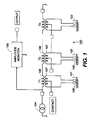
- FIG. 1 is a schematic of a current driven test and measurement system in accord with the present invention.
- FIG. 2 is a schematic of a voltage driven test and measurement system in accord with the present invention.
- FIG. 3 is a detailed circuit schematic of a preferred embodiment of the present invention.
- FIG. 1 there is shown a schematic of a current driven test and measurement system 100 in accordance with the present invention.
- a series of electrical contact pairs 101-103 are split into two individually spring loaded contact pins 106.
- Each pair 101-103 of contact pins 106 are connected to the primary 107 of a small center, tapped transformer, designated T1 to Tn respectively.
- the transformer secondaries 108 are driven with an alternating current (AC) source 104.
- Additional circuitry, for example, an amplitude monitor 105 then monitors the looking-in impedance of the transformer secondaries in series.
- the corresponding transformer primary 107 is short-circuited, thus, causing the reflected secondary impedance to become extremely low.
- This contact condition is monitored continuously for all contacts, during all test and measurement periods. This same scheme can be used for all signal, power and ground leads, without restriction.
- the contact testing is absolutely continuous, while all measurements are running. That is, the two halves of the primary are series opposing from the point of view of all signal power and ground currents, which therefore link zero net flux with the transformer core. Consequently the transformer is itself effectively invisible to both the signal and power paths, while the contact is completely floating electrically.
- the effects from primary leakage inductance are evident, they can be circumvented by placing two equal small capacitors across the two halves of each transformer primary, if necessary. To the extent that there is any small residual coupling between different contacts, via the transformer primary to secondary capacitances, this can be circumvented by the use of transformers with electrostatic shields.
- a small oscillatory mechanical motion for the whole probe head can be employed to in effect automatically "wipe" the contacts until all low impedances are obtained.
- a simple wiping action could be an automatic part of the lowering motion of the probe head, as would be understood by a person skilled in the art.
- the scheme shown in Fig. I drives all the transformers T1 through Tn in series from a single alternating current source 104 and then monitors the sum of the resulting voltage drops across the secondaries.
- a current driven source is viable, there are some advantages with utilizing a voltage to drive the transformers, as shown in Fig. 2.
- This system 200 of Fig. 2 adjusts the radio frequency (RF) drive voltage amplitude until the current measured at a current measurement device 203 is a certain fixed current as produced from a current reference 202, and the quantity measured by the amplitude monitor 105 is the voltage required to obtain that fixed current.
- RF radio frequency
- One major advantage of the voltage driven system 200 is that in actual operation all of the transformer primaries and all of the secondaries, T1 to Tn, are simultaneously, in effect, short-circuited. This has the result of minimizing any potential crosstalk effects without requiring the use of electrostatically shielded transformers, although such transformers can always be used, if desired.
- FIG. 3 there is shown a detailed circuit schematic of one preferred embodiment 300 of the present invention.
- the component values and part numbers given in the parts list to follow, i.e., resistance, capacitance, inductance and transistor part numbers, are illustrative only, and may be varied without straying from the scope of the invention disclosed herein.
- the operational amplifiers utilized are well known in the art. Essentially, an operational amplifier is a high gain device and many suitable amplifiers are available commercially. Although only one transformer 303 is shown rather then several transformers in series, one for each circuit, the system 300 operates as the system 200 in Fig. 2, with a monitoring circuit section 301, a radio frequency drive voltage input section 302, and a current measuring circuit section 304 which includes a current reference circuit.
- the oscillating input circuit 302 includes an L1C1 resonant circuit coupled to an operational amplifier 305 which is powered by two twelve volt (12V) inputs of opposite polarity.
- the L1C1 tank circuit is preferably tuned to a frequency of 160 kHz.
- the operational amplifier 305 is positively biased by an output from the current measurement circuit 304 through a transistor, Q1, coupled to a resistor R1 through which a negative twelve volts (-12V) is introduced.
- the output of the amplifier 305 is coupled to a variable resistor RV1, a feedback loop to the non-inverting (+) input of the amplifier 305 at terminal 3, and to the monitoring section 301 at the base of transistor Q6.
- the center tapped 1:1 transformer 303 is preferably one milli-henry (1mH), and both contact legs 306 and 307 are shunted by capacitors C2 and C3, respectively, to circumvent the effect of leakage inductance at the transformer primary from high frequency oscillation voltages.
- a transformer 303 was utilized having a physical configuration of 1.3 cm square by 7 mm high and a primary to secondary capacitance of -3 Pico-farads (pf) has been utilized.
- the current measuring section 304 is tuned to reduce the effect of any spurious signals arising from the applied driving and switching voltages at the contacts.
- the current measuring section 304 is coupled directly to the transformer 303 secondary leg, labeled "2", through a capacitor C4 to the emitter of transistor Q3 and resistor R5.
- the collector of Q3 is coupled to a resistor R4 which is in turn coupled to a twelve volt (12V) supply applied through resistor R2 to the collector of transistor Q2.
- the base of transistor Q2 is tapped to variable resistor RV1, and the emitter is coupled to a negative twelve volt (-12V) supply through resistor R3 and coupled to the transformer 303 secondary leg, labeled "1".
- the collector of transistor Q3 is coupled through capacitor C5 to an L2C6 tank circuit.
- transistor Q4 has its emitter coupled to a resistor R6, its collector coupled to a resistor R7, and its base coupled to the L2C6 tank circuit and capacitor C5. Coupled across resistor R6, are the collector and base of transistor Q5. The emitter of transistor Q5 is coupled to a capacitor C7 and a resistor R8. Coupled from resistors R8 and R7 is resistor R10 which is in turn coupled to capacitors C9 and C10 which are coupled to a negative twelve (12) volt supply. Resistors R10 and R8 are coupled to an inverting (-) input to an operational amplifier 306 with positive and negative biasing voltages of twelve (12) volts.
- the non-inverting (+) input of the amplifier 306 is preferably tied to ground, as shown, and the output is partially fed-back through a capacitor C8 to the inverting (-) input of the amplifier 306, i.e., a negative feedback loop, and fed through a resistor R9 to the emitter of transistor Q1.
- the demanded constant radio frequency (RF) current flowing from pin-to-pin, i.e., 306 and 307, at each contact is defined by resistors R8 and R10 and is set at a value of 2 milli-amperes, although it could readily be higher if desired.
- This current provides the RF driving voltage, which itself is monitored, and ensures that the contacts themselves remain electrically quiet.
- the monitoring circuit section 301 produces current pulses, at the 160 kHz carrier frequency, whenever the sum total of all the probe contact resistances rises above the preset maximum value.
- the output of amplifier 305 is fed as a base input to transistor Q6, which has its emitter coupled to resistors R11 and R13 and its collector coupled to a resistor R15, which in turn is coupled to a negative twelve (12) volt supply.
- Resistor R15 is coupled to the emitter of transistor Q7, and the junction at resistor R11 and the collector of Q6 is coupled to a voltage divider, made up of resistors R13 and R14, which are in turn coupled to the base of transistor Q7.
- Resistor R11 is commonly coupled to resistor R12, the emitter of transistor Q8, capacitors C11, C12, and C13, and a twelve (12) volt supply.
- Resistor R12 is tied to the collector of transistor Q7 and the base of transistor Q8.
- the emitter of transistor Q8, is fed back through a biasing diode D1 to the base of transistor Q8, and coupled to the output point through a resistor R16.
- the preferred circuit embodiment 300 of Fig. 3 is preferably fabricated in surface mount technology to occupy an area of only 3 cm by 4 cm, so as to be readily mounted close to any multi-pin probe head for actual high reliability applications.
Landscapes
- Physics & Mathematics (AREA)
- General Physics & Mathematics (AREA)
- Testing Of Short-Circuits, Discontinuities, Leakage, Or Incorrect Line Connections (AREA)
- Measurement Of Resistance Or Impedance (AREA)
- Testing Electric Properties And Detecting Electric Faults (AREA)
Abstract
Description
- R1
- 10K
- R2
- 100
- R3
- 2.7K
- R4
- 1K
- R5
- 2.7K
- R6
- 4.7K
- R7
- 100
- R8
- 22K
- R9
- 8.2K
- R10
- 120K
- R11
- 4.7K
- R12
- 2.2K
- R13
- 4.7K
- R14
- 220
- R15
- 10K
- R16
- 4.7K
- RV1
- 2.2K
- C1
- 10nf
- C2
- 1nf
- C3
- 1nf
- C4
- 0.1uf
- C5
- 10nf
- C6
- 10nf
- C7
- 1nf
- C8
- 01uf
- C9
- 47uf
- C10
- 0.1uf
- C11
- 0.1uf
- C12
- 47uf
- C13
- 0.1uf
- D1
- ZC2800
- L1
- 100uh
- L2
- 100uh
- Q1
- 2N3906
- Q2
- 2N3904
- Q3
- 2N3904
- Q4
- 2N3906
- Q5
- 2N3904
- Q6
- 2N3904
- Q7
- 2N3904
- Q8
- 2N3906
- 1C1
- LM3080
- 1C2
- LF351
Claims (20)
- A monitoring system for continuously monitoring the integrity of a made electrical connection comprising:a transformer having a primary winding and secondary winding, said primary winding having a given tap and being coupled to said electrical connection;an energy source coupled to said secondary winding and said given tap; anda monitoring device coupled between said energy source and said transformer for detecting said made connection.
- The system in accordance with claim 1, wherein said energy source is an alternating current source.
- The system in accordance with claim 1, wherein the monitoring device is an amplitude monitor for indicating that said electrical contact is made when the measured reflected secondary impedance across said transformer is less than a predetermined value.
- The system in accordance with claim 1, wherein said energy source is an alternating voltage source.
- The system in accordance with claim 4, further including a given current reference coupled to said secondary winding with a polarity opposing the current generated in said secondary winding.
- The system in accordance with claim 5, wherein the monitoring device measures the given current reference when said connection with said electrical contact is made.
- The system in accordance with claim 1, further including a contact area and wherein said electrical connection comprises an electrical contact which is capable of being automatically positioned against a given contact area with a small oscillatory mechanical motion so as to ensure that a low impedance is reflected in said secondary winding.
- The system in accordance with claim 1, wherein said electrical connection comprising a plurality of electrical contacts, each having a dual contact split pin arrangement.
- The system in accordance with claim 8, further including a plurality of transformers having a primary winding and a secondary winding, each of said primary windings being coupled to separate ones of said plurality of electrical contacts and having a given tap, and each of the secondary windings being coupled in a series circuit arrangement.
- The system in accordance with claim 9, wherein the energy source is coupled across said series circuit arrangement.
- A electrical contact system for monitoring the integrity of electrical connections comprising:an electrical contact having a dual contact split pin arrangement;a transformer having a primary winding and secondary winding, said primary winding having a given tap and being coupled to said electrical contact, said transformer having a given winding to winding coupling capacitance;a voltage driving circuit with a given oscillation characteristic coupled to said secondary winding;a current reference circuit coupled to said secondary winding and said voltage driving circuit; and,a monitoring circuit coupled to said voltage driving circuit operable so as to indicate a current from said current reference circuit when said electrical connection through said electrical contact is made.
- The electrical contact system in accordance with claim 11, further including capacitors, each shunting a leg of the split pin so as to minimize the effects of inductance leakage at said primary winding of said transformer.
- The electrical contact system in accordance with claim 11, wherein said voltage driving circuit includes an inductor capacitor circuit, tuned to said given oscillation characteristic, and input to an operational amplifier.
- The electrical contact system in accordance with claim 13, wherein said operational amplifier is positively biased with a current output from said current reference circuit.
- The electrical contact system in accordance with claim 13, wherein an output from said operational amplifier is coupled to an input to said operational amplifier, said output coupled to said monitoring circuit and coupled to a variable resistor.
- The electrical contact system in accordance with claim 11, wherein said secondary winding of said transformer is coupled to said voltage driving circuit through a transistor circuit coupled to said variable resistor.
- The electrical contact system in accordance with claim 11, wherein said monitoring circuit includes three cascaded stages of transistor circuits biased by a voltage supply.
- The electrical contact system in accordance with claim 11, wherein said current reference circuit includes an operational amplifier having inputs coupled to said secondary winding and an output coupled to said voltage driving circuit.
- The electrical contact system in accordance with claim 18, wherein said current reference circuit is coupled to three stages of transistor circuits which are coupled to said secondary winding and coupled to said operational amplifier
- The electrical contact system in accordance with claim 19, wherein said three stages of transistor circuits includes an inductor capacitor circuit tuned to a given frequency.
Applications Claiming Priority (2)
| Application Number | Priority Date | Filing Date | Title |
|---|---|---|---|
| US714908 | 1991-06-14 | ||
| US08/714,908 US5744965A (en) | 1996-09-17 | 1996-09-17 | System for continuously monitoring the integrity of an electrical contact connection |
Publications (2)
| Publication Number | Publication Date |
|---|---|
| EP0829731A2 true EP0829731A2 (en) | 1998-03-18 |
| EP0829731A3 EP0829731A3 (en) | 1998-04-29 |
Family
ID=24871945
Family Applications (1)
| Application Number | Title | Priority Date | Filing Date |
|---|---|---|---|
| EP97307001A Withdrawn EP0829731A3 (en) | 1996-09-17 | 1997-09-09 | Ultra high reliability electrical contacts |
Country Status (3)
| Country | Link |
|---|---|
| US (1) | US5744965A (en) |
| EP (1) | EP0829731A3 (en) |
| JP (1) | JPH10142283A (en) |
Cited By (3)
| Publication number | Priority date | Publication date | Assignee | Title |
|---|---|---|---|---|
| WO2000048020A3 (en) * | 1999-02-10 | 2000-12-28 | Geco As | Open circuit detector |
| EP1816710A1 (en) * | 2006-02-03 | 2007-08-08 | MGE UPS Systems | Device for connecting several electrical supply devices in parallel |
| WO2020245519A1 (en) | 2019-06-06 | 2020-12-10 | Psa Automobiles Sa | Electrical system and method for diagnosing a faulty electrical connection in an electrical system |
Families Citing this family (7)
| Publication number | Priority date | Publication date | Assignee | Title |
|---|---|---|---|---|
| US6268734B1 (en) * | 2000-03-10 | 2001-07-31 | Analog Devices, Inc. | Operational amplifier input offset voltage and input bias current test circuit |
| US6646519B2 (en) | 2001-05-07 | 2003-11-11 | Viewsonics, Inc. | RF equalizer |
| US7183871B2 (en) * | 2001-05-07 | 2007-02-27 | Viewsonics, Inc | Bi-directional access point |
| US6603301B2 (en) * | 2001-07-26 | 2003-08-05 | Agilent Technologies, Inc. | Multiple range current measurement system with low power dissipation, fast setting time, and low common mode voltage error |
| US20110169520A1 (en) * | 2010-01-14 | 2011-07-14 | Mks Instruments, Inc. | Apparatus for measuring minority carrier lifetime and method for using the same |
| CN110391554A (en) * | 2018-04-23 | 2019-10-29 | 金一凡 | A smart socket that can monitor contact impedance |
| US12306251B2 (en) * | 2019-11-13 | 2025-05-20 | Phoenix Contact Gmbh & Co. Kg | Contact-monitoring device |
Family Cites Families (9)
| Publication number | Priority date | Publication date | Assignee | Title |
|---|---|---|---|---|
| US3303418A (en) * | 1963-05-27 | 1967-02-07 | Westinghouse Electric Corp | Electrical apparatus for testing joints having four voltage probes |
| US3626248A (en) * | 1970-02-06 | 1971-12-07 | Struthers Dunn | Contact monitoring system |
| JPS5040904B1 (en) * | 1970-11-20 | 1975-12-27 | ||
| US3705401A (en) * | 1972-02-11 | 1972-12-05 | Francis A Scott | Electrical alarm system |
| US3906491A (en) * | 1973-05-14 | 1975-09-16 | Federal Sign And Signal Corp | Electronic alarm and emergency voice communication system |
| US4100380A (en) * | 1976-03-12 | 1978-07-11 | Federal Signal Corporation | Supervisory circuit for monitoring speaker coils |
| JPS57204459A (en) * | 1981-06-12 | 1982-12-15 | Hitachi Ltd | Connected monitoring circuit |
| US4649821A (en) * | 1986-01-03 | 1987-03-17 | Quantic Industries, Inc. | Electrical circuit continuity test apparatus for firing unit |
| DE3928775A1 (en) * | 1989-08-31 | 1991-03-07 | Kommunikations Elektronik | CIRCUIT ARRANGEMENT FOR CONTROLLING THE LEVEL OF ELECTRICAL SIGNALS |
-
1996
- 1996-09-17 US US08/714,908 patent/US5744965A/en not_active Expired - Lifetime
-
1997
- 1997-09-09 EP EP97307001A patent/EP0829731A3/en not_active Withdrawn
- 1997-09-17 JP JP9251749A patent/JPH10142283A/en active Pending
Cited By (4)
| Publication number | Priority date | Publication date | Assignee | Title |
|---|---|---|---|---|
| WO2000048020A3 (en) * | 1999-02-10 | 2000-12-28 | Geco As | Open circuit detector |
| EP1816710A1 (en) * | 2006-02-03 | 2007-08-08 | MGE UPS Systems | Device for connecting several electrical supply devices in parallel |
| WO2020245519A1 (en) | 2019-06-06 | 2020-12-10 | Psa Automobiles Sa | Electrical system and method for diagnosing a faulty electrical connection in an electrical system |
| FR3097057A1 (en) | 2019-06-06 | 2020-12-11 | Psa Automobiles Sa | FAULTY ELECTRICAL CONNECTION DIAGNOSIS PROCESS IN AN ELECTRICAL SYSTEM |
Also Published As
| Publication number | Publication date |
|---|---|
| JPH10142283A (en) | 1998-05-29 |
| EP0829731A3 (en) | 1998-04-29 |
| US5744965A (en) | 1998-04-28 |
Similar Documents
| Publication | Publication Date | Title |
|---|---|---|
| US11454651B2 (en) | Automatic probe ground connection checking techniques | |
| AU675644B2 (en) | Near-end communications line characteristic measuring system | |
| US5744965A (en) | System for continuously monitoring the integrity of an electrical contact connection | |
| CA1194405A (en) | Submersible pump telemetry system | |
| US5625292A (en) | System for measuring the integrity of an electrical contact | |
| EP0279577B1 (en) | Transformer testing | |
| US6236220B1 (en) | Method for the testing of an inductive resonant circuit | |
| EP0385672A2 (en) | Induction coil driver | |
| US4998059A (en) | Dual demodulating circuit tracer | |
| US5287062A (en) | Reference voltage measuring bridge for a device for monitoring and measuring the insulation of a DC voltage electrical mains system | |
| EP0349168A2 (en) | Circuit element measuring apparatus | |
| US4070615A (en) | Compensation indicator for attenuation probe | |
| US5164662A (en) | Detection of radio frequency emissions | |
| JP2000506612A (en) | Parameter measuring equipment for electronic devices | |
| JPH01501251A (en) | Pseudo-resonance control device for observation coils for nuclear magnetic resonance | |
| US4344034A (en) | Selective/ground neutralizing metal detector | |
| US3437920A (en) | Transducer circuits with frequency-amplitude control | |
| US4103335A (en) | Line synchronized interrupt generator | |
| US6348802B1 (en) | Device for enhancing contact checking | |
| Argüelles et al. | Signature analysis for fault detection of mixed-signal ICs based on dynamic power-supply current | |
| US3331969A (en) | Circuit for reproduction of a plurality of similar low-level d.c. signals | |
| JP3294395B2 (en) | Partial discharge light balance detector | |
| CN111398727B (en) | Noise filtering equipment and electromagnetic compatibility test system | |
| CN109188149B (en) | Electric signal acquisition device | |
| Bergervoet et al. | EMC measurements with an optical link |
Legal Events
| Date | Code | Title | Description |
|---|---|---|---|
| PUAI | Public reference made under article 153(3) epc to a published international application that has entered the european phase |
Free format text: ORIGINAL CODE: 0009012 |
|
| PUAL | Search report despatched |
Free format text: ORIGINAL CODE: 0009013 |
|
| AK | Designated contracting states |
Kind code of ref document: A2 Designated state(s): DE FR GB |
|
| AK | Designated contracting states |
Kind code of ref document: A3 Designated state(s): AT BE CH DE DK ES FI FR GB GR IE IT LI LU MC NL PT SE |
|
| 17P | Request for examination filed |
Effective date: 19981015 |
|
| AKX | Designation fees paid |
Free format text: DE FR GB |
|
| RBV | Designated contracting states (corrected) |
Designated state(s): DE FR GB |
|
| 17Q | First examination report despatched |
Effective date: 20020307 |
|
| STAA | Information on the status of an ep patent application or granted ep patent |
Free format text: STATUS: THE APPLICATION IS DEEMED TO BE WITHDRAWN |
|
| 18D | Application deemed to be withdrawn |
Effective date: 20030225 |