EP0831611A2 - Dispositif de traitement de signaux pour le multiplexage/démultiplexage de fréquences - Google Patents
Dispositif de traitement de signaux pour le multiplexage/démultiplexage de fréquences Download PDFInfo
- Publication number
- EP0831611A2 EP0831611A2 EP97306520A EP97306520A EP0831611A2 EP 0831611 A2 EP0831611 A2 EP 0831611A2 EP 97306520 A EP97306520 A EP 97306520A EP 97306520 A EP97306520 A EP 97306520A EP 0831611 A2 EP0831611 A2 EP 0831611A2
- Authority
- EP
- European Patent Office
- Prior art keywords
- processing apparatus
- signal processing
- digital signal
- bands
- sub
- Prior art date
- Legal status (The legal status is an assumption and is not a legal conclusion. Google has not performed a legal analysis and makes no representation as to the accuracy of the status listed.)
- Granted
Links
Images


Classifications
-
- H—ELECTRICITY
- H04—ELECTRIC COMMUNICATION TECHNIQUE
- H04J—MULTIPLEX COMMUNICATION
- H04J1/00—Frequency-division multiplex systems
- H04J1/02—Details
- H04J1/04—Frequency-transposition arrangements
- H04J1/05—Frequency-transposition arrangements using digital techniques
Definitions
- This invention relates to digital signal processing apparatus for frequency demultiplexing or multiplexing.
- the invention especially relates to such processing apparatus for use on-board a satellite.
- a satellite will have receiving beams and transmitting beams.
- the on-board processor may demultiplex the received uplink channels into sub-bands, switch them to different downlink channels where desired, multiplex the sub-bands of the respective downlink channels, change the frequency of the downlink channels, amplify the channels, that the downlink beams may be transmitted.
- the Applicants have previously proposed a digital signal processing apparatus for multiplexing or demultiplexing a narrowband channel, typically 4 MHz, with sub-bands typically 36 KHz in width (EP-A-0 695 054).
- Figure 2 shows the general scheme of the demultiplexer.
- the sub-bands are isolated by means of a polyphase filter and linked FFT units 4a, 4b, which perform a relatively coarse filtering operation.
- the frequency response of the polyphase filter/FFT for extracting sub-band 0 is shown in Figure 3b.
- the pass band is centred on the desired channel, but the transition bands are relatively relaxed and actually extend over the adjacent sub-band on each side.
- the units 4a, 4b have a similar frequency response centred on each sub-band K-1, 0, 1 etc of the narrowband input channel, which is a complex FDM (frequency division multiplex) of K-channels ( Figure 3a).
- the relaxed transition bands reduce the complexity of the polyphase filter/FFT implementation, and hence reduce its cost.
- the first digital filter 3 consisted of an imaged low pass (for example half band) digital filter (producing an output as shown in Figure 3e) and an imaged high pass (for example, half band) digital filter (producing an output as shown in Figure 3f).
- This was obtained by using a digital filter such as an FIR filter having the desired tight (prototype) filter shape, say, that centred on sub-band k 0, and then padding the impulse response with zero coefficients to produce multiple images of that tight filter shape.
- the alternate frequency slots for the low pass case are nulled out ( Figure 3e). So are those for the high pass case ( Figure 3f).
- Each low and high pass prototype impulse response are each padded with (K/2-1) zeros between each coefficient to produce K/2 images of the prototype filter each.
- the transition bands ( Figure 3b) now lie in the nulled out regions of the spectrum. Not only is the bank of fine filters unnecessary, but now the maximum possible decimation of K can be performed in each ofthe two polyphase filter/FFT units 4a, 4b, as shown in Figure 3d.
- the transition bands of adjacent sub-bands are now wholly aliased with each sub-band, but this does not matter since they do not contain any energy
- the invention provides a digital signal processing apparatus for frequency demultiplexing a wideband channel into equally spaced sub-bands, comprising a fine filtering stage which includes low pass digital filter means and high pass digital filter means, each being arranged to null out alternate frequency slots leaving only even numbered and odd numbered sub-bands, and a coarse filtering stage connected to the output ofthe fine filtering stage which includes digital filter means for isolating the even numbered sub-bands and the odd numbered sub-bands, wherein there is provided a serial-to-parallel converter having an input for wide band signal samples and outputs for a plurality of sub-sampled signals, and wherein the low pass filter means and the high pass filter means each comprise a respective filter in each parallel branch.
- the invention also provides a digital signal processing apparatus for frequency multiplexing a plurality of sub-bands into a wide band channel comprising a block coarse filtering stage which includes digital filter means for combining even numbered sub-bands, and for combining odd numbered sub-bands, and a fine filtering stage connected to the output of the coarse filtering stage, which fine filtering stage includes low pass digital filter means and high pass digital filter means, each arranged to null out alternate frequency slots leaving only the even numbered sub-bands and the odd numbered sub-bands, wherein there is provided a parallel-to-serial converter having an input for the sub-band signal samples and an output for the wideband signal samples, and wherein the low pass filter means and the high pass filter means each comprise a respective filter in each parallel branch.
- each parallel branch permits the use of slower, cheaper processors e.g. CMOS of lower power even though the overall data rate can be chosen to correspond to a wideband channel.
- processors e.g. CMOS of lower power
- each individual low pass and high pass filter in each branch only processes separated, not consecutive wideband signal samples, it turns out that the same output samples are produced by the individual low pass and high filters in the branches after the signals in the branches have been recombined as for the block low pass and block high pass filter of EP-A-0 695 054 since zeros in the impulse response also mean that adjacent samples are not combined together to produce the successive output samples.
- the satellite on board which both forms of digital signal processing apparatus according to the invention may be used may have two uplink beams and two downlink beams, each being wideband, for example, (of the order of 250-500 MHz) bandwidth.
- a portion of the spectrum of a beam processed in accordance with the invention is shown in Figure 1.
- the full spectrum ofthe channel could extend, say, from 11.5 GHz to 12 GHz for the uplink and 10.5 GHz to 11 GHz for the downlink.
- the spectrum is allocated in blocks of 36 MHz as shown, or 72 or 108 MHz.
- the channel would be demultiplexed into frequency slots of these widths, amplified, switched between beams if desired, multiplexed and transmitted.
- Prior analogue multiplexers/demultiplexers would require dedicated filters for 36 MHz, 72 MHz and 108 MHz, to be switched from the ground. It will be noted that with the digital processor of the invention, the 36 MHz band is made up using four 9 MHz slots, and the whole ofthe 250-500 MHz bandwidth is defined using 9 MHz slots spaced at 10.5 MHz spacing.
- the demultiplexing/multiplexing is contiguous i.e. a relatively wideband channel in the FDM is processed in the form of the constituent sub-bands which span the bandwidth occupied by the channel. The digital processing therefore gives greater flexibility in addition to the advantage of dispensing with bulky analogue filters.
- the known demultiplexer consists of an analogue-to-digital converter (ADC) 2 which digitises a narrowband channel at IF frequency at sampling rate f s .
- ADC analogue-to-digital converter
- the spectrum of the sampled signals in Figure 2 or EP-A-0 695 054 extends over a certain bandwidth of frequencies, both positive and negative.
- the invention can be best understood by considering the known demultiplexer of Figure 2 with a real FDM such as is illustrated in Figure 4a i.e. without an anti-aliasing filter.
- the second (coarse) block filtering stage 4a, 4b extracts the K channels with a frequency response with relaxed transition bands (Figure 4b). This is preceded by a first (fine) block filtering stage 3, which has a low pass characteristic to produce the response at Figure 4c and a high pass characteristic to produce the response of Figure 4d.
- Each unit 4a, 4b is connected to one of the low pass, high pass outputs of the block fine filtering stage.
- Each unit is a linked polyphase/FFT processor.
- the impulse responses of the FIR low pass, high pass filters 3 are respectively padded with zeros (K-1) to produce K even numbered and K odd numbered images of the basic, tight, frequency response (the prototype) of which the images are copies.
- the transition bands of the units 4a, 4b lie in the nulled out regions of the spectrum between the images in the low and high pass filters.
- the individually extracted outputs from the units 4a, 4b can be decimated by the maximum amount of 2K as shown schematically by boxes 5a-5d, although this operation actually takes place in the polyphase/FFT filter.
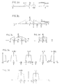
- FIG 5 is a conceptual representation of the first form of digital signal processing apparatus in accordance with the invention
- the block high pass filter and block low pass digital filter of Figure 2 can be replaced by individual low 3a(1-L) and high pass 3b(1-L) filters in parallel branches which are fed cyclically with samples (SIPO 6) and from which the processed samples are cyclically combined (PISO 7a, 7b).
- the imaged tight filter function 3 is used to pre-process data prior to demultiplexing or post-process data following multiplexing.
- the design is based around a prototype low pass filter which would be suitable for extracting a single slot centred at DC from an FDM of two slots as shown in Figure 7a.
- the prototype low pass filter can be simply converted into a high pass filter as shown in Figure 8a.
- the only change to the filter coefficients is the negation of all the taps except the centre tap.
- the same filter can therefore be used to generate both the low and high pass versions of a signal using identical partial products. It is merely the final summation that determines which band is generated.
- Figure 9a shows the low pass filter imaged by a factor of two. This filter is now suitable for extracting two slots from an FDM of four and, in general, the imaging factor will be equal to half the number of slots within the FDM.
- the imaged high pass version can again be derived from the equivalent low pass version by subtracting the centre tap instead of adding it.
- the resultant filter would now be suitable for extracting the other two slots from a four slot FDM.
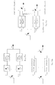
- Figure 5 shows a conceptual representation of the first form of digital signal processing apparatus for frequency demultiplexing a wideband channel into K-sub-bands.
- ADC 1 feeds a serial-to-parallel converter 6.
- the first sample from ADC 1 goes to branch 1, the second to branch 2, the Lth to branch L, and the L+1th to branch 1.
- the first digital filter 3 is implemented as pairs of filters 3a(1), 3b(1) to 3a(L), 3b(L).
- the parts 3a correspond to the output 3 of Figure 2 which produced the low pass response of Figure 3a
- the parts 3b correspond to the output 3 of Figure 2 which produced the high pass response of Figure 3f
- the low pass outputs are converted into a serial data stream in parallel-to-serial converter 7a, and likewise the high pass outputs in parallel-to-serial converter 7b (corresponding to the outputs of the first digital filter 3 which pass to 4a and 4b respectively).
- second digital filter 4a, 4b are each implemented by processors 4a(1) to 4a(L) and 4b(1) to 4b(L) in parallel branches, fed by serial-to-parallel converters 8a, 8b
- converters 7a, 8a, 7b, 8b are omitted, and it has surprisingly been found that 3a(1) can be connected directly to 4a(1), 3b(1) to 4b(1) etc. This will be discussed in more detail below.
- the parallel implementation of the first form demultiplexer will now be explained in greater detail.
- the first digital filter 3 of Figure 2 is a single rate structure with no decimation or interpolation between the input and output sampling rates.
- the unit sample response of the digital filter 3 is that of a prototype FIR filter (a 1/2-band design) with an additional L-1 zeros padded between each coefficient, L being the interpolation factor between the sampling rate of the prototype 1/2-band filter and the sampling rate of the input.
- L the interpolation factor between the sampling rate of the prototype 1/2-band filter and the sampling rate of the input.
- the realisation ofthe first digital filter 3 as parallel low-rate branches in this general case can be understood by considering the polyphase decomposition of the input signal, as shown in Figure 11a.
- Each output sample from the first digital filter 3 of Figure 2 is the sum of L branch computations, L-1 of which are identically zero on any output sample due to the zero-padded nature of the unit sample response.
- the summation can be replaced with a commutator and the input signal also delivered to each branch with a commutator, as shown in Figure 11b.
- Each of the two full rate outputs from the first digital filter is processed in a second digital filter.
- the second digital filter applies a 2K-point FFT on successive windowed, aliased, segments of its input which are prepared by the WOLA filter.
- the key to the realisation of the second digital filter in this way is to exploit the fact that the 2K-point FFT can be performed as a 2D FFT based on a row-column decomposition of the samples with L rows (processors 4a(1) to 4a(L): 4b(1) to 4b(L)) and (2K/L) columns (processors 4a', 4b'), where the placing of samples into the rows is performed in natural order using a commutator.
- N second digital filter 6K
- the length of the segment of window in each branch is 6n.
- the multiplication and aliasing operation in each branch is performed as a set of 2n FIR-type convolutions generating the 2n inputs to the row FFTs.
- the 2D decomposition uses the Cooley-Tukey algorithm, which requires an intermediate set of twiddles between the 2n-point row FFTs and the (K/n)-point column FFTs. Because each second digital filter performs a partial FFT, only about half the twiddles are required on each.
- Figure 6 shows the generic form of the parallel architecture for the high speed front-end demultiplexer which divides the input FDM into K sub-bands.
- the branch processors are identical apart from the 6n (in this example) distinct coefficients in each partial WOLA.
- the branch inputs are real, and the outputs are in general complex.
- the demultiplexing is completed with the set of 2n complex-complex (K/n)-point column FFTs (4a', 4b'), each of which synthesises K/2n useful outputs.
- the twiddles W 2K are shown acting on the inputs to the column FFT processors.
- the input FDM could comprise 8 channel slots on a 42 MHz spacing, in an even stacking configuration.
- the passband of the analogue filter providing the input to the ADC 2 spans 7 slots with a bandwidth of 294 MHz; the shape factor of the AAF is therefore 9/7 and the sampling frequency is 672 Msps.
- Twiddles between the row FFTs and the column FFTs can be eliminated if a Good-Thomas decomposition is used; this however imposes certain constraints on the architecture.
- parameter description fs sampled bandwidth of real input is fs/2 b
- ADC sample wordlength K number of sub-band slots n,m integers > 0 K/n number of branch chains nfs/K sampling rate of branch chain input (real) fs/K sampling rate of branch chain outputs (complex) 2nm number of column FFT processors K/nm size of complex-complex column FFT
- sample deinterleaver serial-to-parallel converter
- interleaver parallel-to-serial converter
- the ADC will have 2 output channels, at 8 bits each. Each channel is divided into 7 separate sample streams with 14 flip-flops/bit, giving a total 1-14 deinterleaver.
- the complete unit therefore requires 224 flip-flops, each drawing 3.05 mW to give a total of 683 mW. Adding I/O the total power for the 1-14 SIPO unit in GaAs would be less than 5 W.
- Figures 5 and 6 may have a useful bandwidth of 252 MHz, comprising six 36 MHz channels on a 42 MHz channel centre spacing.
- the Good-Thomas algorithms may be used to provide 23 useful 9 MHz sub-bands spanning 240 MHz which lie in the positive frequency half of the AAF passband.
- the sub-bands are on a 10.5 MHz spacing and are oversampled by 2 on the output of the demultiplexer at 21 Msps. Note that by going to a finer granularity the shape factor of the AAF and AIF filters can be increased and at the same time the overall sampling rate reduced by more than 10% from 672 Msps to 588 Msps. Figure 1 shows such an organisation of the channel.
- the parallel implementation permits the use of processors in the parallel branches operating at no more than 42 Msps, so that cheaper CMOS processors e.g. on ASICs can be used, whereas if an attempt was made to implement the embodiments in the serial form of Figure 2, data processing speeds of at least 588 Msps would be required, which would not be practicable to implement in today's technology even if expensive GaAs processors were used.
- Multiplexers according to the invention work in an inverse manner to the demultiplexers described with the caveat that in the multiplexer mode the first digital filter is bypassed if the baseband inputs are oversampled by 2.
- the processing apparatus is suitable for transparent as well as regenerative satellites.
Landscapes
- Physics & Mathematics (AREA)
- Electromagnetism (AREA)
- Engineering & Computer Science (AREA)
- Computer Networks & Wireless Communication (AREA)
- Signal Processing (AREA)
- Complex Calculations (AREA)
- Time-Division Multiplex Systems (AREA)
- Image Processing (AREA)
- Compression, Expansion, Code Conversion, And Decoders (AREA)
Applications Claiming Priority (2)
| Application Number | Priority Date | Filing Date | Title |
|---|---|---|---|
| GB9619537A GB2317537B (en) | 1996-09-19 | 1996-09-19 | Digital signal processing apparatus for frequency demultiplexing or multiplexing |
| GB9619537 | 1996-09-19 |
Publications (3)
| Publication Number | Publication Date |
|---|---|
| EP0831611A2 true EP0831611A2 (fr) | 1998-03-25 |
| EP0831611A3 EP0831611A3 (fr) | 2002-08-14 |
| EP0831611B1 EP0831611B1 (fr) | 2003-10-29 |
Family
ID=10800149
Family Applications (1)
| Application Number | Title | Priority Date | Filing Date |
|---|---|---|---|
| EP97306520A Expired - Lifetime EP0831611B1 (fr) | 1996-09-19 | 1997-08-26 | Dispositif de traitement de signaux pour le multiplexage/démultiplexage de fréquences |
Country Status (6)
| Country | Link |
|---|---|
| US (1) | US6118794A (fr) |
| EP (1) | EP0831611B1 (fr) |
| AT (1) | ATE253275T1 (fr) |
| CA (1) | CA2214869C (fr) |
| DE (1) | DE69725818T2 (fr) |
| GB (1) | GB2317537B (fr) |
Cited By (3)
| Publication number | Priority date | Publication date | Assignee | Title |
|---|---|---|---|---|
| EP1032155A3 (fr) * | 1999-02-26 | 2004-09-15 | Northrop Grumman Corporation | Décalage cyclique pour un canaliseur numérique |
| WO2012120137A1 (fr) | 2011-03-10 | 2012-09-13 | Astrium Limited | Traitement de données rso |
| US10551162B2 (en) | 2015-05-06 | 2020-02-04 | North Carolina State University | Code-modulated phased-array interferometric imaging |
Families Citing this family (15)
| Publication number | Priority date | Publication date | Assignee | Title |
|---|---|---|---|---|
| US7986729B2 (en) * | 1999-10-28 | 2011-07-26 | Lightwaves Systems, Inc. | High bandwidth data transport system |
| US6990060B2 (en) * | 2000-02-11 | 2006-01-24 | Bae Systems | Polyphase-discrete fourier transform (DFT) sub-band definition filtering architecture |
| GB2366494A (en) | 2000-09-05 | 2002-03-06 | Mitel Corp | Dividing bandwidth into sub-bands prior to implementing an FFT in a high data rate communications network |
| SE0202159D0 (sv) | 2001-07-10 | 2002-07-09 | Coding Technologies Sweden Ab | Efficientand scalable parametric stereo coding for low bitrate applications |
| CA2359771A1 (fr) * | 2001-10-22 | 2003-04-22 | Dspfactory Ltd. | Systeme et methode de synthese audio en temps reel necessitant peu de ressources |
| DE60202881T2 (de) | 2001-11-29 | 2006-01-19 | Coding Technologies Ab | Wiederherstellung von hochfrequenzkomponenten |
| GB2382961B (en) * | 2001-12-05 | 2005-01-19 | Matsushita Electric Industrial Co Ltd | Multirate digital transceiver |
| SE0202770D0 (sv) | 2002-09-18 | 2002-09-18 | Coding Technologies Sweden Ab | Method for reduction of aliasing introduces by spectral envelope adjustment in real-valued filterbanks |
| JP5528358B2 (ja) * | 2008-03-10 | 2014-06-25 | ニューランズ・インコーポレーテッド | 広帯域信号処理の方法、システムおよび装置 |
| EP2522073A4 (fr) | 2010-02-12 | 2014-06-11 | Newlans Inc | Composants radioélectriques analogiques à large bande |
| US9007128B2 (en) | 2010-11-01 | 2015-04-14 | Newlans, Inc. | Method and apparatus for power amplifier linearization |
| US8970252B2 (en) | 2010-11-08 | 2015-03-03 | Newlans, Inc. | Field programmable analog array |
| US8779832B2 (en) | 2011-11-01 | 2014-07-15 | Newlans, Inc. | Wideband signal processing |
| JP6012066B2 (ja) * | 2012-08-01 | 2016-10-25 | Necスペーステクノロジー株式会社 | チャネライザ及び信号処理方法 |
| CN104662799A (zh) | 2012-09-05 | 2015-05-27 | 纽兰斯公司 | 双二阶校准 |
Family Cites Families (6)
| Publication number | Priority date | Publication date | Assignee | Title |
|---|---|---|---|---|
| US4138730A (en) * | 1977-11-07 | 1979-02-06 | Communications Satellite Corporation | High speed FFT processor |
| ATE63413T1 (de) * | 1986-04-14 | 1991-05-15 | Siemens Ag | Demultiplexstufe eines digitalsignal¨bertragungsger|tes. |
| US5247515A (en) * | 1991-01-28 | 1993-09-21 | Rockwell International Corporation | Apparatus for extracting one from many multiplexed signals |
| US5425027A (en) * | 1993-01-04 | 1995-06-13 | Com21, Inc. | Wide area fiber and TV cable fast packet cell network |
| US5535240A (en) * | 1993-10-29 | 1996-07-09 | Airnet Communications Corporation | Transceiver apparatus employing wideband FFT channelizer and inverse FFT combiner for multichannel communication network |
| GB9414664D0 (en) * | 1994-07-20 | 1994-09-07 | British Aerospace | Digital signal processing apparatus |
-
1996
- 1996-09-19 GB GB9619537A patent/GB2317537B/en not_active Expired - Fee Related
-
1997
- 1997-08-26 DE DE69725818T patent/DE69725818T2/de not_active Expired - Lifetime
- 1997-08-26 AT AT97306520T patent/ATE253275T1/de not_active IP Right Cessation
- 1997-08-26 EP EP97306520A patent/EP0831611B1/fr not_active Expired - Lifetime
- 1997-09-08 CA CA002214869A patent/CA2214869C/fr not_active Expired - Fee Related
- 1997-09-16 US US08/931,478 patent/US6118794A/en not_active Expired - Lifetime
Cited By (4)
| Publication number | Priority date | Publication date | Assignee | Title |
|---|---|---|---|---|
| EP1032155A3 (fr) * | 1999-02-26 | 2004-09-15 | Northrop Grumman Corporation | Décalage cyclique pour un canaliseur numérique |
| WO2012120137A1 (fr) | 2011-03-10 | 2012-09-13 | Astrium Limited | Traitement de données rso |
| JP2014510913A (ja) * | 2011-03-10 | 2014-05-01 | アストリアム リミテッド | Sarデータ処理 |
| US10551162B2 (en) | 2015-05-06 | 2020-02-04 | North Carolina State University | Code-modulated phased-array interferometric imaging |
Also Published As
| Publication number | Publication date |
|---|---|
| GB2317537B (en) | 2000-05-17 |
| DE69725818D1 (de) | 2003-12-04 |
| GB2317537A (en) | 1998-03-25 |
| CA2214869A1 (fr) | 1998-03-19 |
| US6118794A (en) | 2000-09-12 |
| GB9619537D0 (en) | 1996-10-30 |
| EP0831611A3 (fr) | 2002-08-14 |
| CA2214869C (fr) | 2004-02-24 |
| DE69725818T2 (de) | 2004-08-12 |
| EP0831611B1 (fr) | 2003-10-29 |
| ATE253275T1 (de) | 2003-11-15 |
Similar Documents
| Publication | Publication Date | Title |
|---|---|---|
| EP0831611B1 (fr) | Dispositif de traitement de signaux pour le multiplexage/démultiplexage de fréquences | |
| US6091704A (en) | Digital multi-channel demultiplexer/multiplexer (MCD/M) architecture | |
| US4691292A (en) | System for digital multiband filtering | |
| US5493581A (en) | Digital down converter and method | |
| CA2061685C (fr) | Appareil et methode de traitement de signaux numeriques | |
| EP0549451B1 (fr) | Dispositif de démultiplexage en fréquence à filtres numériques | |
| EP1114516B1 (fr) | Amelioration de flexibilite de l'algorithme de convolution rapide modifie | |
| EP2184866B1 (fr) | Transpondeur transparent numérique flexible | |
| EP0623265A1 (fr) | Procede et moyens pour transmultiplexer des signaux entre des terminaux de reception de signaux et des radiocanaux | |
| JP2653830B2 (ja) | 音声秘話装置 | |
| US5699363A (en) | Digital signal processing apparatus | |
| Saramaki et al. | Multirate systems and filterbanks | |
| JPH10215237A (ja) | 離散時間信号に対する多重化装置および多重化システム | |
| Fliege | Computational efficiency of modified DFT polyphase filter banks | |
| US5293382A (en) | Method for FDMA signal multiplexing and demultiplexing | |
| JP2000022658A (ja) | 複数搬送波変調方式 | |
| CA2122652C (fr) | Filtre demi-bande pour demultiplexeur de groupe cellulaire | |
| US5247515A (en) | Apparatus for extracting one from many multiplexed signals | |
| WO2008050766A1 (fr) | Dispositif de démultiplexage de signal numérique et dispositif de multiplexage de signaux numériques | |
| US20090304031A1 (en) | Digital signal demultiplexing device and multiplexing device | |
| Harris et al. | Interleaving different bandwidth narrowband channels in perfect reconstruction cascade polyphase filter banks for efficient flexible variable bandwidth filters in wideband digital transceivers | |
| JPH0884049A (ja) | ディジタル処理信号分割器及びディジタル処理信号合成器 | |
| CN119363306B (zh) | 基于二次多相分解和数据抽取的信道化器 | |
| WO1991014310A1 (fr) | Appareil et procede de traitement des signaux numeriques | |
| CA1184608A (fr) | Methode de transposition de la frequence de sous-bandes |
Legal Events
| Date | Code | Title | Description |
|---|---|---|---|
| PUAI | Public reference made under article 153(3) epc to a published international application that has entered the european phase |
Free format text: ORIGINAL CODE: 0009012 |
|
| AK | Designated contracting states |
Kind code of ref document: A2 Designated state(s): AT BE CH DE DK ES FI FR GB GR IE IT LI LU MC NL PT SE |
|
| AX | Request for extension of the european patent |
Free format text: AL;LT;LV;RO;SI |
|
| RAP1 | Party data changed (applicant data changed or rights of an application transferred) |
Owner name: MATRA MARCONI SPACE UK LIMITED |
|
| PUAL | Search report despatched |
Free format text: ORIGINAL CODE: 0009013 |
|
| RIC1 | Information provided on ipc code assigned before grant |
Free format text: 7H 04L 5/06 A, 7H 04J 1/05 B |
|
| AK | Designated contracting states |
Kind code of ref document: A3 Designated state(s): AT BE CH DE DK ES FI FR GB GR IE IT LI LU MC NL PT SE |
|
| AX | Request for extension of the european patent |
Free format text: AL;LT;LV;RO;SI |
|
| 17P | Request for examination filed |
Effective date: 20030128 |
|
| GRAH | Despatch of communication of intention to grant a patent |
Free format text: ORIGINAL CODE: EPIDOS IGRA |
|
| AKX | Designation fees paid |
Designated state(s): AT BE CH DE DK ES FI FR GB GR IE IT LI LU MC NL PT SE |
|
| AXX | Extension fees paid |
Extension state: SI Payment date: 20030128 Extension state: RO Payment date: 20030128 Extension state: LV Payment date: 20030128 Extension state: LT Payment date: 20030128 Extension state: AL Payment date: 20030128 |
|
| GRAS | Grant fee paid |
Free format text: ORIGINAL CODE: EPIDOSNIGR3 |
|
| GRAA | (expected) grant |
Free format text: ORIGINAL CODE: 0009210 |
|
| AK | Designated contracting states |
Kind code of ref document: B1 Designated state(s): AT BE CH DE DK ES FI FR GB GR IE IT LI LU MC NL PT SE |
|
| AX | Request for extension of the european patent |
Extension state: AL LT LV RO SI |
|
| PG25 | Lapsed in a contracting state [announced via postgrant information from national office to epo] |
Ref country code: NL Free format text: LAPSE BECAUSE OF FAILURE TO SUBMIT A TRANSLATION OF THE DESCRIPTION OR TO PAY THE FEE WITHIN THE PRESCRIBED TIME-LIMIT Effective date: 20031029 Ref country code: LI Free format text: LAPSE BECAUSE OF FAILURE TO SUBMIT A TRANSLATION OF THE DESCRIPTION OR TO PAY THE FEE WITHIN THE PRESCRIBED TIME-LIMIT Effective date: 20031029 Ref country code: FI Free format text: LAPSE BECAUSE OF FAILURE TO SUBMIT A TRANSLATION OF THE DESCRIPTION OR TO PAY THE FEE WITHIN THE PRESCRIBED TIME-LIMIT Effective date: 20031029 Ref country code: CH Free format text: LAPSE BECAUSE OF FAILURE TO SUBMIT A TRANSLATION OF THE DESCRIPTION OR TO PAY THE FEE WITHIN THE PRESCRIBED TIME-LIMIT Effective date: 20031029 Ref country code: BE Free format text: LAPSE BECAUSE OF FAILURE TO SUBMIT A TRANSLATION OF THE DESCRIPTION OR TO PAY THE FEE WITHIN THE PRESCRIBED TIME-LIMIT Effective date: 20031029 Ref country code: AT Free format text: LAPSE BECAUSE OF FAILURE TO SUBMIT A TRANSLATION OF THE DESCRIPTION OR TO PAY THE FEE WITHIN THE PRESCRIBED TIME-LIMIT Effective date: 20031029 |
|
| REG | Reference to a national code |
Ref country code: GB Ref legal event code: FG4D |
|
| REG | Reference to a national code |
Ref country code: CH Ref legal event code: EP |
|
| REG | Reference to a national code |
Ref country code: IE Ref legal event code: FG4D |
|
| REF | Corresponds to: |
Ref document number: 69725818 Country of ref document: DE Date of ref document: 20031204 Kind code of ref document: P |
|
| PG25 | Lapsed in a contracting state [announced via postgrant information from national office to epo] |
Ref country code: SE Free format text: LAPSE BECAUSE OF FAILURE TO SUBMIT A TRANSLATION OF THE DESCRIPTION OR TO PAY THE FEE WITHIN THE PRESCRIBED TIME-LIMIT Effective date: 20040129 Ref country code: GR Free format text: LAPSE BECAUSE OF FAILURE TO SUBMIT A TRANSLATION OF THE DESCRIPTION OR TO PAY THE FEE WITHIN THE PRESCRIBED TIME-LIMIT Effective date: 20040129 Ref country code: DK Free format text: LAPSE BECAUSE OF FAILURE TO SUBMIT A TRANSLATION OF THE DESCRIPTION OR TO PAY THE FEE WITHIN THE PRESCRIBED TIME-LIMIT Effective date: 20040129 |
|
| PG25 | Lapsed in a contracting state [announced via postgrant information from national office to epo] |
Ref country code: ES Free format text: LAPSE BECAUSE OF FAILURE TO SUBMIT A TRANSLATION OF THE DESCRIPTION OR TO PAY THE FEE WITHIN THE PRESCRIBED TIME-LIMIT Effective date: 20040209 |
|
| NLV1 | Nl: lapsed or annulled due to failure to fulfill the requirements of art. 29p and 29m of the patents act | ||
| LTIE | Lt: invalidation of european patent or patent extension |
Effective date: 20031029 |
|
| REG | Reference to a national code |
Ref country code: CH Ref legal event code: PL |
|
| ET | Fr: translation filed | ||
| PG25 | Lapsed in a contracting state [announced via postgrant information from national office to epo] |
Ref country code: LU Free format text: LAPSE BECAUSE OF NON-PAYMENT OF DUE FEES Effective date: 20040826 Ref country code: IE Free format text: LAPSE BECAUSE OF NON-PAYMENT OF DUE FEES Effective date: 20040826 Ref country code: GB Free format text: LAPSE BECAUSE OF NON-PAYMENT OF DUE FEES Effective date: 20040826 |
|
| PG25 | Lapsed in a contracting state [announced via postgrant information from national office to epo] |
Ref country code: MC Free format text: LAPSE BECAUSE OF NON-PAYMENT OF DUE FEES Effective date: 20040831 |
|
| PLBE | No opposition filed within time limit |
Free format text: ORIGINAL CODE: 0009261 |
|
| STAA | Information on the status of an ep patent application or granted ep patent |
Free format text: STATUS: NO OPPOSITION FILED WITHIN TIME LIMIT |
|
| 26N | No opposition filed |
Effective date: 20040730 |
|
| GBPC | Gb: european patent ceased through non-payment of renewal fee |
Effective date: 20040826 |
|
| REG | Reference to a national code |
Ref country code: IE Ref legal event code: MM4A |
|
| REG | Reference to a national code |
Ref country code: FR Ref legal event code: TP Ref country code: FR Ref legal event code: CD |
|
| PG25 | Lapsed in a contracting state [announced via postgrant information from national office to epo] |
Ref country code: PT Free format text: LAPSE BECAUSE OF NON-PAYMENT OF DUE FEES Effective date: 20040329 |
|
| REG | Reference to a national code |
Ref country code: FR Ref legal event code: CD |
|
| PGFP | Annual fee paid to national office [announced via postgrant information from national office to epo] |
Ref country code: DE Payment date: 20120822 Year of fee payment: 16 Ref country code: IT Payment date: 20120823 Year of fee payment: 16 Ref country code: FR Payment date: 20120906 Year of fee payment: 16 |
|
| REG | Reference to a national code |
Ref country code: DE Ref legal event code: R119 Ref document number: 69725818 Country of ref document: DE |
|
| PG25 | Lapsed in a contracting state [announced via postgrant information from national office to epo] |
Ref country code: DE Free format text: LAPSE BECAUSE OF NON-PAYMENT OF DUE FEES Effective date: 20140301 |
|
| REG | Reference to a national code |
Ref country code: FR Ref legal event code: ST Effective date: 20140430 |
|
| PG25 | Lapsed in a contracting state [announced via postgrant information from national office to epo] |
Ref country code: IT Free format text: LAPSE BECAUSE OF NON-PAYMENT OF DUE FEES Effective date: 20130826 |
|
| PG25 | Lapsed in a contracting state [announced via postgrant information from national office to epo] |
Ref country code: FR Free format text: LAPSE BECAUSE OF NON-PAYMENT OF DUE FEES Effective date: 20130902 |
|
| REG | Reference to a national code |
Ref country code: DE Ref legal event code: R119 Ref document number: 69725818 Country of ref document: DE Effective date: 20140301 |