EP0834241B1 - Circuit electronique - Google Patents
Circuit electronique Download PDFInfo
- Publication number
- EP0834241B1 EP0834241B1 EP97906334A EP97906334A EP0834241B1 EP 0834241 B1 EP0834241 B1 EP 0834241B1 EP 97906334 A EP97906334 A EP 97906334A EP 97906334 A EP97906334 A EP 97906334A EP 0834241 B1 EP0834241 B1 EP 0834241B1
- Authority
- EP
- European Patent Office
- Prior art keywords
- circuit arrangement
- mode
- power supply
- capacitive
- voltage
- Prior art date
- Legal status (The legal status is an assumption and is not a legal conclusion. Google has not performed a legal analysis and makes no representation as to the accuracy of the status listed.)
- Expired - Lifetime
Links
Images

Classifications
-
- H—ELECTRICITY
- H05—ELECTRIC TECHNIQUES NOT OTHERWISE PROVIDED FOR
- H05B—ELECTRIC HEATING; ELECTRIC LIGHT SOURCES NOT OTHERWISE PROVIDED FOR; CIRCUIT ARRANGEMENTS FOR ELECTRIC LIGHT SOURCES, IN GENERAL
- H05B41/00—Circuit arrangements or apparatus for igniting or operating discharge lamps
- H05B41/14—Circuit arrangements
- H05B41/26—Circuit arrangements in which the lamp is fed by power derived from DC by means of a converter, e.g. by high-voltage DC
- H05B41/28—Circuit arrangements in which the lamp is fed by power derived from DC by means of a converter, e.g. by high-voltage DC using static converters
- H05B41/288—Circuit arrangements in which the lamp is fed by power derived from DC by means of a converter, e.g. by high-voltage DC using static converters with semiconductor devices and specially adapted for lamps without preheating electrodes, e.g. for high-intensity discharge lamps, high-pressure mercury or sodium lamps or low-pressure sodium lamps
- H05B41/292—Arrangements for protecting lamps or circuits against abnormal operating conditions
Definitions
- the invention relates to a circuit arrangement for igniting and operating a discharge lamp, provided with
- Such a circuit arrangement is known from electronic ballasts of the HF-B TLD and HF-P TLD types, make Philips, designed for igniting and operating fluorescent lamps, and ballast EMC 035-S01, make Philips, suitable for igniting and operating a high-pressure discharge lamp, in particular a metal halide lamp.
- the filter means serve to ensure that the ballast complies with requirements known inter alia under the designation EN55015. It is achieved in this manner that the amount of interference signals occurring, especially in the frequency range from 9 kHz to 30 MHz, remains below a maximum admissible level under certain defined conditions.
- the inductive means in the known ballast comprise mutually coupled first and second windings in the first and second voltage conduction branch, respectively, forming a common-mode coil and a separate inductance as a differential- mode coil.
- the separate inductance may be provided in one of the voltage conduction branches as a separate self-inductance.
- a technical equivalent is an embodiment in the form of two mutually coupled windings distributed over the two voltage conduction branches.
- the capacitive filter means comprise a differential-mode capacitor which connects the first and second voltage conduction branches and is placed between the common-mode coil and the differential-mode coil, and which at the same time forms a series circuit with a common-mode capacitor which also forms part of the capacitive filter means.
- the common-mode capacitor forms a connection between at least part of the inductive means and the ground terminal.
- the differential-mode capacitor with the differential-mode inductance forms a differential-mode filter
- the common-mode capacitor with the common-mode coil forms a common-mode filter.
- the common-mode capacitor in the known circuit arrangement is formed by a single capacitor. It is alternatively possible for the capacitive filter means to be formed by two capacitors, each connected to the ground terminal, while the first and second voltage conduction branches are each connected to one of the two capacitors.
- the filter means of the known ballast constitute a satisfactory measure for complying with said requirements, it is found to be impossible by these means to have the circuit arrangement also comply with requirements according to EN55022 on the admissible quantity of interference in the frequency range from 30 MHz to 1 GHz. This is a problem.
- the invention has for its object to provide a measure for eliminating this problem.
- a circuit arrangement of the kind mentioned in the opening paragraph is for this purpose characterized in that the input terminals as well as the output terminals are connected by means of the capacitive filter means both to one another and to the ground terminal, in that a bead is included in each one of the third and fourth voltage conduction branches, and in that further common-mode capacitive means are present between the inductive means and the switch mode power supply.
- the inductive means are constructed as first and second windings coupled with leakage in the first and second voltage conduction branches, respectively.
- the coupled inductance together with the further common-mode capacitive means thus forms part of the common-mode filter for the frequency range from 9 kHz to 30 MHz, while the leakage inductance forms part of the differential-mode filter.
- a bead was found to be particularly suitable for counteracting interference signals at higher frequencies owing to the substantial absence of a parasitic capacitance.
- Particularly suitable beads for a high-frequency filter are ferrite beads having a comparatively high ohmic impedance for the frequency range from 30 MHz to 1 GHz.
- the operation of the differential-mode filter for the high-frequency range is further benefited when two beads are placed, which beads are arranged in different voltage conduction branches of mutually differing polarities.
- the circuit arrangement is provided with an igniter circuit for generating ignition voltage pulses for igniting a high-pressure discharge lamp.
- a circuit is often provided with a primary winding of a pulse transformer of which a secondary winding is arranged in series with an output terminal.
- the pulse transformer provides for the upward transformation in the secondary winding of a pulse formed in the igniter circuit to a level suitable and sufficient for igniting the lamp.
- the secondary winding is placed between a bead and the relevant output terminal. This advantageously prevents as much as possible that high-frequency signals caused by the ignition pulses form a load on the switch mode power supply. This is realized in a very advantageous manner in that the third and the fourth voltage conduction branches are both provided with a bead.
- high-pressure discharge lamps are operated at a voltage of periodically alternating polarity.
- a circuit arrangement for igniting and operating such a lamp and provided with a switch mode power supply comprises a commutator for this purpose, which is connected to the third and fourth voltage conduction branches.
- the commutator will comprise at least two, often even four switching elements which are made conducting and non-conducting in alternation. It is preferable here that the beads are placed between the switching elements and the output terminals.
- a switch mode power supply comprises a rectifier device for forming a DC voltage from the AC voltage delivered by the connected supply source. It is surprisingly achieved through the placement of the further common-mode capacitive means between the ground terminal and a DC voltage pole that any leakage current to earth through the further common-mode capacitive means will be considerably smaller than if the further common-mode capacitive means were connected to an AC voltage pole. This renders it possible to give the further common-mode capacitive means a higher capacitance value, which results in an improved common-mode filter action.
- Fig. 1 shows a circuit arrangement for igniting and operating a discharge lamp 9.
- the circuit arrangement shown relates to a ballast suitable for operating a high-pressure discharge lamp, in particular a metal halide lamp, and provided with
- the filter means 4 serve to achieve that the ballast complies with requirements known inter alia under the designation EN55015. It is ensured thereby that the amount of interference signals occurring, especially in the frequency range from 9 kHz to 30 MHz, remains below a maximum admissible level under certain defined conditions.
- the inductive means comprise mutually coupled first and second windings 401, 402 in the first and second voltage conduction branches, respectively, forming a common-mode coil and a separate inductance 403, in the form of two windings distributed over the two voltage conduction branches and mutually coupled, acting as a differential-mode coil.
- the capacitive filter means comprise a differential-mode capacitor 41 which interconnects the first and second voltage conduction branches and which is placed between the common-mode coil 400 and the differential-mode coil 403, and at the same time forms a series circuit with a common-mode capacitor 42 which also forms part of the capacitive filter means.
- the common-mode capacitor forms a connection between at least part of the inductive means and the ground terminal 3.
- the differential-mode capacitor 41 together with a further differential-mode capacitor 44 and the inductance 403 forms a differential-mode filter, while the common-mode capacitor 42 and the common-mode coil 400 form a common-mode filter.
- the common-mode capacitor in the known circuit arrangement is formed by a single capacitor.
- the circuit arrangement shown in Fig. 2 is a circuit arrangement according to the invention. Parts cotresponding to those of Fig. 1 have been given the same reference numerals.
- the inductive means are here constructed as first and second windings 40A, 40B coupled with leakage and arranged in the first and second voltage conduction branches, respectively.
- the coupled inductance together with the further common-mode capacitive means 42 thus forms part of the common-mode filter for the frequency range from 9 kHz to 30 MHz, whereas the leakage inductance forms part of the differential-mode filter.
- the input terminals 1, 2 and the output terminals 7, 8 are connected both to one another and to the ground terminal 3 via capacitive filter means 41, 42 and 45, 46, respectively.
- a bead 47, 48 is included in each of the voltage conduction branches 10, 11, while further common-mode capacitive means 43 are present between the inductive means 400 and the switch mode power supply I.
- the switch mode power supply is shown in more detail in Fig. 3.
- the switch mode power supply comprises a rectifier device 15 for forming a DC voltage from the AC voltage delivered by the supply source connected, followed by a first DC-DC converter 16 and a second DC-DC converter 17.
- the converter 17 is subsequently connected to a commutator 20.
- the rectifier device 15, the DC-DC converters 16, 17, and the commutator 20 are interconnected by DC voltage conductors 151 and 152.
- the DC-DC converters are each provided with controlled switching means which are rendered conducting and non-conducting periodically by means of control signals generated in a control circuit 18.
- a measuring impedance 19 is included between the two DC-DC converters in the DC voltage conductor 152 for forming the control signals.
- the commutator 20 which is connected to the third and fourth voltage conduction branches comprises four switching elements 21, 22, 23, 24 which are rendered conducting and non-conducting alternately.
- the commutator is further provided with an igniter circuit 25 for generating ignition voltage pulses.
- the circuit comprises a primary winding 261 of a pulse transformer 26 of which a secondary winding 262 is placed in series with output terminal 8 between output terminal 8 and filter capacitor 45. Bead 47 is here placed between the switching elements 21, 22 and the output terminal 7. Bead 48 is placed between the switching elements 23, 24 and the secondary winding 262.
- the circuit arrangement is suitable for igniting and operating a metal halide lamp, for example of the CDM 35W type, make Philips, with a power rating of 39 W, designed for connection to a 220 V, 50 Hz supply source.
- the filter means are built up from the following components: windings 40A,40B bead 46,47 self-inductance 2*13mH leakage ind.
- the first DC-DC converter 16 is an upconverter which forms a DC voltage of 400 V for supplying the second DC-DC converter 17 from the full-wave rectified supply voltage.
- the converter 17 is constructed as a Buck or downconverter and forms a controlled current generator during stable lamp operation. Lamp voltage is approximately 90 V during stable lamp operation.
- the controlled switching means of the two DC-DC converters are each rendered conducting and non-conducting alternately with a high frequency, in the range of 17 kHz to 0.2 MHz, during stable lamp operation.
- the switching elements of the commutator switch with a substantially constant frequency of 150 Hz so as to be conducting and non-conducting alternately.
- the secondary winding 262 of the pulse transformer 26 has 76 turns and accordingly has such a great parasitic capacitance that it plays no role of any importance in suppressing interference signals.
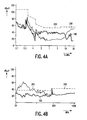
- Fig. 4A,B is a frequency diagram of the quantity of interference signal generated by the embodiment described during operation of a CDM 35W lamp (make Philips with a nominal wattage of 39 W), measured by means of a peak measurement.
- the signal intensity is plotted in a usual unit on the vertical axis and the frequency on the horizontal axis.
- Fig. 4A shows the frequency range covered by the standard EN55015.
- Fig. 4B relates to the frequency range covered by the standard EN55022.
- the specific measuring technique suitable and indeed required for each frequency range may give rise to differences in value of the measured interference signal at the same frequency when measured in accordance with EN55015 or EN55022.
- Curve 100 represents the intensity of the measured signal and curve 200 is the maximum admissible intensity according to EN55015 and EN55022. Since curve 100 remains below curve 200 over the entire frequency range, it will be obvious that the circuit arrangement according to the invention complies with both standards EN55015 and EN55022.
- curve 300 is shown representing the signal intensity when the known
Landscapes
- Circuit Arrangements For Discharge Lamps (AREA)
Abstract
Claims (6)
- Dispositif de circuit pour l'amorçage et le fonctionnement d'une lampe à décharge 9 comprenantdes première (1) et deuxième(2) bornes d'entrée pour la connexion d'une source d'alimentation, et une borne de masse,des moyens de filtrage en mode différentiel et en mode commun (4) dans lesquels sont incorporés des moyens inductifs (400, 403) et des moyens de filtrage capacitifs (41, 42, 44),une alimentation de puissance en mode de commutation (I) connectée à la première borne d'entrée (1) et à la deuxième borne d'entrée (2), respectivement à l'aide d'une première branche de conduction de tension (5) et d'une deuxième branche de conduction de tension (6), etdes première (7) et deuxième (8) bornes de sortie pour la connexion de la lampe à décharge (9), lesquelles bornes de sortie sont connectées à l'alimentation de puissance en mode de commutation (I) à l'aide de respectivement une troisième branche de conduction de tension (10) et d'une quatrième branche de conduction de tension (11), caractérisé en ce que les bornes d'entrée (42) ainsi que les bornes de sortie (7, 8) sont connectées, à l'aide des moyens de filtrage capacitifs, les unes aux autres ainsi qu'à la borne de masse, en ce qu'une perle (47, 48) est insérée dans chacune des troisième (10) et quatrième (11) branches de conduction de tension, et en ce que d'autres moyens capacitifs en mode commun sont présents entre les moyens inductifs et l'alimentation de puissance en mode de commutation (I).
- Dispositif de circuit selon la revendication 1, caractérisé en ce que les deux perles (47, 48) sont disposées dans différentes branches de conduction de tension (10, 11) présentant des polarités mutuellement différentes.
- Dispositif de circuit selon la revendication 1 ou 2, caractérisé en ce que l'alimentation de puissance en mode de commutation (I) est munie d'un commutateur (20) comprenant des éléments de commutation (21, 22, 23, 24), qui sont rendus alternativement conducteurs et non conducteurs, et en ce que les perles (47, 48) sont placées entre les éléments de commutation et les bornes de sortie (7, 8).
- Dispositif de circuit selon la revendication 1, 2 ou 3, caractérisé en ce que le dispositif de circuit est muni d'un circuit d'amorçage (25) servant à engendrer des impulsions de tension d'amorçage, comprenant un enroulement primaire (261) d'un transformateur d'impulsions dont un enroulement secondaire (262) est connecté en série avec une borne de sortie (8) et en ce que l'enroulement secondaire (262) est placé entre une perle (48) et la borne de sortie en question.
- Dispositif de circuit selon la revendication 1, 2, 3 ou 4, caractérisé en ce que le dispositif de circuit est muni d'un circuit d'amorçage (25) servant à engendrer des impulsions de tension d'amorçage et comprenant un enroulement primaire (261) d'un transformateur d'impulsions (26) dont un enroulement secondaire est connecté en série avec une borne de sortie, et en ce que l'enroulement secondaire est placé entre l'une des bornes de sortie et les moyens de filtrage capacitifs respectifs.
- Dispositif de circuit selon la revendication 1, 2, 3, 4 ou 5, caractérisé en ce que l'alimentation de puissance en mode de commutation (I) est muni d'un dispositif redresseur (15) et d'un conducteur de courant continu, et en ce que les autres moyens capacitifs en mode commun (43) sont connectés entre la borne de masse (3) et le conducteur de courant continu.
Priority Applications (1)
| Application Number | Priority Date | Filing Date | Title |
|---|---|---|---|
| EP97906334A EP0834241B1 (fr) | 1996-04-18 | 1997-03-27 | Circuit electronique |
Applications Claiming Priority (4)
| Application Number | Priority Date | Filing Date | Title |
|---|---|---|---|
| EP96201036 | 1996-04-18 | ||
| EP96201036 | 1996-04-18 | ||
| PCT/IB1997/000315 WO1997039606A1 (fr) | 1996-04-18 | 1997-03-27 | Circuit electronique |
| EP97906334A EP0834241B1 (fr) | 1996-04-18 | 1997-03-27 | Circuit electronique |
Publications (2)
| Publication Number | Publication Date |
|---|---|
| EP0834241A1 EP0834241A1 (fr) | 1998-04-08 |
| EP0834241B1 true EP0834241B1 (fr) | 2002-10-02 |
Family
ID=8223879
Family Applications (1)
| Application Number | Title | Priority Date | Filing Date |
|---|---|---|---|
| EP97906334A Expired - Lifetime EP0834241B1 (fr) | 1996-04-18 | 1997-03-27 | Circuit electronique |
Country Status (5)
| Country | Link |
|---|---|
| US (1) | US5834902A (fr) |
| EP (1) | EP0834241B1 (fr) |
| JP (1) | JPH11509675A (fr) |
| DE (1) | DE69716004T2 (fr) |
| WO (1) | WO1997039606A1 (fr) |
Families Citing this family (7)
| Publication number | Priority date | Publication date | Assignee | Title |
|---|---|---|---|---|
| DE10221631A1 (de) * | 2002-05-15 | 2003-12-04 | Tridonicatco Gmbh & Co Kg | Funkentstördrosseln zur Unterdrückung von Gleichtaktstörungen in einem Elektronischen Vorschaltgerät (EVG) |
| EP1416575A1 (fr) * | 2002-10-30 | 2004-05-06 | STMicroelectronics S.A. | Transformateur à changement de mode |
| JP2009289684A (ja) * | 2008-05-30 | 2009-12-10 | Toshiba Lighting & Technology Corp | 高圧放電灯点灯装置 |
| US9559581B2 (en) * | 2013-04-17 | 2017-01-31 | The Regents Of The University Of Michigan | Single phase bi-directional AC-DC converter with reduced passive components size and common mode electro-magnetic interference |
| DE102014200865A1 (de) * | 2014-01-17 | 2015-07-23 | Osram Gmbh | Schaltungsanordnung zum Betreiben von Lichtquellen |
| CN111162742B (zh) * | 2020-03-04 | 2024-06-18 | 广西微车检智能科技有限公司 | 一种抑制机动车检测装置信号干扰的信号处理系统 |
| WO2023044848A1 (fr) * | 2021-09-26 | 2023-03-30 | 宁德时代新能源科技股份有限公司 | Circuit de commutation et dispositif d'alimentation électrique |
Family Cites Families (5)
| Publication number | Priority date | Publication date | Assignee | Title |
|---|---|---|---|---|
| US4323824A (en) * | 1979-12-21 | 1982-04-06 | Gte Products Corporation | Low voltage fluorescent operating circuit |
| JPS5738594A (en) * | 1980-08-20 | 1982-03-03 | Ushio Electric Inc | Device for firing discharge lamp |
| US5513088A (en) * | 1991-06-14 | 1996-04-30 | Williamson; Floyd | Uninterruptable off-line, isolated flyback topology switch-mode power supply |
| US5586016A (en) * | 1994-07-05 | 1996-12-17 | Motorola, Inc. | Circuit for quickly energizing electronic ballast |
| US5568041A (en) * | 1995-02-09 | 1996-10-22 | Magnetek, Inc. | Low-cost power factor correction circuit and method for electronic ballasts |
-
1997
- 1997-03-12 US US08/815,241 patent/US5834902A/en not_active Expired - Fee Related
- 1997-03-27 EP EP97906334A patent/EP0834241B1/fr not_active Expired - Lifetime
- 1997-03-27 JP JP9536898A patent/JPH11509675A/ja active Pending
- 1997-03-27 WO PCT/IB1997/000315 patent/WO1997039606A1/fr not_active Ceased
- 1997-03-27 DE DE69716004T patent/DE69716004T2/de not_active Expired - Fee Related
Also Published As
| Publication number | Publication date |
|---|---|
| DE69716004D1 (de) | 2002-11-07 |
| DE69716004T2 (de) | 2003-06-18 |
| WO1997039606A1 (fr) | 1997-10-23 |
| EP0834241A1 (fr) | 1998-04-08 |
| JPH11509675A (ja) | 1999-08-24 |
| US5834902A (en) | 1998-11-10 |
Similar Documents
| Publication | Publication Date | Title |
|---|---|---|
| US5023519A (en) | Circuit for starting and operating a gas discharge lamp | |
| US4508996A (en) | High frequency supply system for gas discharge lamps and electronic ballast therefor | |
| EP0758520B1 (fr) | Circuit d'allumage de lampe a decharge haute pression | |
| EP0150536B1 (fr) | Adaptateur de ballast pour le fonctionnement de lampes fluorescentes | |
| EP0834241B1 (fr) | Circuit electronique | |
| EP0507396B1 (fr) | Dispositif de circuit | |
| CA2037667C (fr) | Circuit d'allumage pour lampes a decharge haute pression | |
| EP0702885B1 (fr) | Configuration de circuit | |
| US5986413A (en) | Reliable ignition circuit for a high pressure discharge lamp | |
| US6118227A (en) | High frequency electronic drive circuits for fluorescent lamps | |
| US6005353A (en) | Commutator for a discharge lamp having mutually coupled inductors | |
| EP0702887B1 (fr) | Configuration de circuit | |
| EP0797907B1 (fr) | Montage de circuit | |
| US4701673A (en) | Ballast adaptor for improving operation of fluorescent lamps | |
| US4123690A (en) | Discharge lamp ballast circuit | |
| KR20010113050A (ko) | 스위칭 장치 | |
| CN1189286A (zh) | 电路 | |
| US20030062853A1 (en) | Remote discharge lamp ignition circuitry | |
| CA1228890A (fr) | Lampe a decharge a ballast electronique et courant d'alimentation haute frequence | |
| EP0834213A1 (fr) | Alimentation electrique a mode de commutation |
Legal Events
| Date | Code | Title | Description |
|---|---|---|---|
| PUAI | Public reference made under article 153(3) epc to a published international application that has entered the european phase |
Free format text: ORIGINAL CODE: 0009012 |
|
| AK | Designated contracting states |
Kind code of ref document: A1 Designated state(s): DE FR GB |
|
| 17P | Request for examination filed |
Effective date: 19980423 |
|
| GRAG | Despatch of communication of intention to grant |
Free format text: ORIGINAL CODE: EPIDOS AGRA |
|
| RIC1 | Information provided on ipc code assigned before grant |
Free format text: 7H 05B 41/295 A |
|
| RIC1 | Information provided on ipc code assigned before grant |
Free format text: 7H 05B 41/295 A |
|
| 17Q | First examination report despatched |
Effective date: 20020102 |
|
| GRAG | Despatch of communication of intention to grant |
Free format text: ORIGINAL CODE: EPIDOS AGRA |
|
| GRAH | Despatch of communication of intention to grant a patent |
Free format text: ORIGINAL CODE: EPIDOS IGRA |
|
| GRAH | Despatch of communication of intention to grant a patent |
Free format text: ORIGINAL CODE: EPIDOS IGRA |
|
| GRAA | (expected) grant |
Free format text: ORIGINAL CODE: 0009210 |
|
| AK | Designated contracting states |
Kind code of ref document: B1 Designated state(s): DE FR GB |
|
| REG | Reference to a national code |
Ref country code: GB Ref legal event code: FG4D |
|
| REF | Corresponds to: |
Ref document number: 69716004 Country of ref document: DE Date of ref document: 20021107 |
|
| ET | Fr: translation filed | ||
| PG25 | Lapsed in a contracting state [announced via postgrant information from national office to epo] |
Ref country code: GB Free format text: LAPSE BECAUSE OF NON-PAYMENT OF DUE FEES Effective date: 20030327 |
|
| PLBE | No opposition filed within time limit |
Free format text: ORIGINAL CODE: 0009261 |
|
| STAA | Information on the status of an ep patent application or granted ep patent |
Free format text: STATUS: NO OPPOSITION FILED WITHIN TIME LIMIT |
|
| 26N | No opposition filed |
Effective date: 20030703 |
|
| PG25 | Lapsed in a contracting state [announced via postgrant information from national office to epo] |
Ref country code: DE Free format text: LAPSE BECAUSE OF NON-PAYMENT OF DUE FEES Effective date: 20031001 |
|
| GBPC | Gb: european patent ceased through non-payment of renewal fee |
Effective date: 20030327 |
|
| PG25 | Lapsed in a contracting state [announced via postgrant information from national office to epo] |
Ref country code: FR Free format text: LAPSE BECAUSE OF NON-PAYMENT OF DUE FEES Effective date: 20031127 |
|
| REG | Reference to a national code |
Ref country code: FR Ref legal event code: ST |