EP0835516B1 - Condensateur a couche enterree - Google Patents
Condensateur a couche enterreeInfo
- Publication number
- EP0835516B1 EP0835516B1 EP96912432A EP96912432A EP0835516B1 EP 0835516 B1 EP0835516 B1 EP 0835516B1 EP 96912432 A EP96912432 A EP 96912432A EP 96912432 A EP96912432 A EP 96912432A EP 0835516 B1 EP0835516 B1 EP 0835516B1
- Authority
- EP
- European Patent Office
- Prior art keywords
- buried layer
- dielectric
- layer
- layer capacitor
- capacitor
- Prior art date
- Legal status (The legal status is an assumption and is not a legal conclusion. Google has not performed a legal analysis and makes no representation as to the accuracy of the status listed.)
- Expired - Lifetime
Links
- 239000003990 capacitor Substances 0.000 title claims description 63
- 239000004020 conductor Substances 0.000 claims description 2
- KDLHZDBZIXYQEI-UHFFFAOYSA-N Palladium Chemical compound [Pd] KDLHZDBZIXYQEI-UHFFFAOYSA-N 0.000 description 4
- 238000010276 construction Methods 0.000 description 3
- 238000004519 manufacturing process Methods 0.000 description 3
- 229910052709 silver Inorganic materials 0.000 description 3
- 239000004332 silver Substances 0.000 description 3
- 238000012360 testing method Methods 0.000 description 3
- RYGMFSIKBFXOCR-UHFFFAOYSA-N Copper Chemical compound [Cu] RYGMFSIKBFXOCR-UHFFFAOYSA-N 0.000 description 2
- PXHVJJICTQNCMI-UHFFFAOYSA-N Nickel Chemical compound [Ni] PXHVJJICTQNCMI-UHFFFAOYSA-N 0.000 description 2
- 229910052802 copper Inorganic materials 0.000 description 2
- 239000010949 copper Substances 0.000 description 2
- 238000005520 cutting process Methods 0.000 description 2
- 239000003989 dielectric material Substances 0.000 description 2
- 239000000463 material Substances 0.000 description 2
- 229910052751 metal Inorganic materials 0.000 description 2
- 239000002184 metal Substances 0.000 description 2
- 238000000034 method Methods 0.000 description 2
- 229910052763 palladium Inorganic materials 0.000 description 2
- 229910000679 solder Inorganic materials 0.000 description 2
- 238000005476 soldering Methods 0.000 description 2
- 238000009966 trimming Methods 0.000 description 2
- FYYHWMGAXLPEAU-UHFFFAOYSA-N Magnesium Chemical compound [Mg] FYYHWMGAXLPEAU-UHFFFAOYSA-N 0.000 description 1
- BQCADISMDOOEFD-UHFFFAOYSA-N Silver Chemical compound [Ag] BQCADISMDOOEFD-UHFFFAOYSA-N 0.000 description 1
- RTAQQCXQSZGOHL-UHFFFAOYSA-N Titanium Chemical compound [Ti] RTAQQCXQSZGOHL-UHFFFAOYSA-N 0.000 description 1
- 238000005299 abrasion Methods 0.000 description 1
- JRPBQTZRNDNNOP-UHFFFAOYSA-N barium titanate Chemical compound [Ba+2].[Ba+2].[O-][Ti]([O-])([O-])[O-] JRPBQTZRNDNNOP-UHFFFAOYSA-N 0.000 description 1
- 229910002113 barium titanate Inorganic materials 0.000 description 1
- 230000004888 barrier function Effects 0.000 description 1
- 239000003985 ceramic capacitor Substances 0.000 description 1
- 230000008602 contraction Effects 0.000 description 1
- 238000012937 correction Methods 0.000 description 1
- 238000011161 development Methods 0.000 description 1
- 230000008030 elimination Effects 0.000 description 1
- 238000003379 elimination reaction Methods 0.000 description 1
- PCHJSUWPFVWCPO-UHFFFAOYSA-N gold Chemical compound [Au] PCHJSUWPFVWCPO-UHFFFAOYSA-N 0.000 description 1
- 229910052737 gold Inorganic materials 0.000 description 1
- 239000010931 gold Substances 0.000 description 1
- 238000003698 laser cutting Methods 0.000 description 1
- 229910052749 magnesium Inorganic materials 0.000 description 1
- 239000011777 magnesium Substances 0.000 description 1
- 150000002739 metals Chemical class 0.000 description 1
- 238000012986 modification Methods 0.000 description 1
- 230000004048 modification Effects 0.000 description 1
- 229910052759 nickel Inorganic materials 0.000 description 1
- 239000000523 sample Substances 0.000 description 1
- 239000007787 solid Substances 0.000 description 1
- VEALVRVVWBQVSL-UHFFFAOYSA-N strontium titanate Chemical compound [Sr+2].[O-][Ti]([O-])=O VEALVRVVWBQVSL-UHFFFAOYSA-N 0.000 description 1
Images


Classifications
-
- H—ELECTRICITY
- H01—ELECTRIC ELEMENTS
- H01G—CAPACITORS; CAPACITORS, RECTIFIERS, DETECTORS, SWITCHING DEVICES, LIGHT-SENSITIVE OR TEMPERATURE-SENSITIVE DEVICES OF THE ELECTROLYTIC TYPE
- H01G9/00—Electrolytic capacitors, rectifiers, detectors, switching devices, light-sensitive or temperature-sensitive devices; Processes of their manufacture
- H01G9/004—Details
- H01G9/04—Electrodes or formation of dielectric layers thereon
-
- H—ELECTRICITY
- H01—ELECTRIC ELEMENTS
- H01G—CAPACITORS; CAPACITORS, RECTIFIERS, DETECTORS, SWITCHING DEVICES, LIGHT-SENSITIVE OR TEMPERATURE-SENSITIVE DEVICES OF THE ELECTROLYTIC TYPE
- H01G4/00—Fixed capacitors; Processes of their manufacture
- H01G4/002—Details
- H01G4/255—Means for correcting the capacitance value
-
- H—ELECTRICITY
- H01—ELECTRIC ELEMENTS
- H01G—CAPACITORS; CAPACITORS, RECTIFIERS, DETECTORS, SWITCHING DEVICES, LIGHT-SENSITIVE OR TEMPERATURE-SENSITIVE DEVICES OF THE ELECTROLYTIC TYPE
- H01G4/00—Fixed capacitors; Processes of their manufacture
- H01G4/002—Details
- H01G4/018—Dielectrics
- H01G4/06—Solid dielectrics
-
- Y—GENERAL TAGGING OF NEW TECHNOLOGICAL DEVELOPMENTS; GENERAL TAGGING OF CROSS-SECTIONAL TECHNOLOGIES SPANNING OVER SEVERAL SECTIONS OF THE IPC; TECHNICAL SUBJECTS COVERED BY FORMER USPC CROSS-REFERENCE ART COLLECTIONS [XRACs] AND DIGESTS
- Y10—TECHNICAL SUBJECTS COVERED BY FORMER USPC
- Y10T—TECHNICAL SUBJECTS COVERED BY FORMER US CLASSIFICATION
- Y10T29/00—Metal working
- Y10T29/43—Electric condenser making
- Y10T29/435—Solid dielectric type
Definitions
- This invention relates generally to capacitors and more particularly to a ceramic capacitor which utilizes a buried layer.
- Prior art relating to solid state capacitors includes such patents as U.S. Patent 4 665 465 to Tanabe and U.S. Patent 5 107 394 to Naito et al. Construction of these capacitors includes multiple electrode layers which are fastened by means of a soldering process to a mechanical end cap. The soldering process introduces a degree of unreliability in a capacitor as a result of residual stresses formed in the capacitor during its manufacture. Additional unreliability results from stresses which are imposed on a solder joint due to differential rates of thermal expansion and contraction of various components of the capacitor including: the electrode, the dielectric material, the solder material and the end cap; when the capacitor is exposed to temperature variations and extremes during use.
- US-A-5 170 317 describes a multilayer capacitor with an additional correction electrode embedded within dielectric layers, having dimensions smaller than the dielectric layers and being spaced from contact with any electrical conductor.
- Another object of the present invention is to provide a buried layer capacitor which is highly reliable.
- Another object of the present invention is to provide a buried layer capacitor which is capable of highly reliable operation over a broad range of operating temperatures.
- Yet another object of the present invention is to provide a buried layer capacitor which can be manufactured in quantity at a low unit cost while maintaining high levels of quality.
- a buried layer capacitor which is defined by the features of claim 1. It includes a planar electrode layer mounted between a pair of dielectric layers. Length and width dimensions of the dielectric layers are slightly greater than corresponding length and width dimensions of the electrode layer and the electrode layer generally is centered with respect to the dielectric layers. One layer of the pair of dielectric layers has a pair of spaced apart leads. The dielectric layer which is attached to the leads has a selected thickness which allows the dielectric layer, in combination with the electrode layer, to develop a desired value of capacitance between the leads.
- the pair of spaced apart leads is replaced by a pair of metallized areas and the dielectric layer in combination with the electrode layer develop a desired value of capacitance between the two metallized areas.
- the metallized areas facilitate mounting the buried layer capacitor on a circuit board while using minimum surface area of the circuit board.
- the metallized areas extend onto end portions of the dielectric layer in order to facilitate testing of the capacitor.
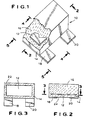
- a buried layer capacitor 10 made in accordance with the present invention, which includes an electrode layer 12, a first dielectric layer 14, a second dielectric layer 16 and a pair of leads 18, 20.
- the dielectric layers 14, 16 are generally rectangular and as is shown in Figs. 1 and 3, the electrode layer 12 also is generally rectangular, with length and width dimensions which are somewhat smaller than corresponding length and width dimensions of the dielectric layers 14, 16.
- the electrode layer 12 is planar and generally is centered relative to the dielectric layers 14, 16 resulting in a border, generally designated by the reference numeral 22, which surrounds the periphery of the electrode layer 12.
- the electrode layer 12 thus is completely contained or buried in the dielectric layers 14, 16.
- the electrode layer may be silver, gold, nickel, copper or palladium or another high conductivity metal.
- the leads 18, 20 are attached to a bottom surface 24 of the dielectric layer 14.
- the leads 18, 20 are each planar and are made of any one of a number of metals which have desirable combination of stiffness and conductivity. Appropriate materials for the leads have been found to be copper and silver.
- the dielectric layers 14, 16 are made of any one of a number of dielectric materials such as magnesium titanate, strontium titanate or barium titanate.
- the first dielectric layer 14 is disposed between the electrode layer 12 and the leads 18, 20.
- the dielectric layer 14, in combination with the electrode layer 12 and the leads 18, 20, allows development of capacitance between the leads 18 , 20.
- the buried layer capacitor 10 of Figs. 1-5 typically has the following dimensions which should be considered as given by way of illustration only and should not be considered as limiting in any way.
- Overall length of the capacitor 10 is in an order of 0.05 inches, its width is in an order of 0.05 inches, its height is in an order of 0.02 inches.
- Thickness of the dielectric layer 14 is in an order of 0.003 inches and thickness of the dielectric layer 16 is in an order of 0.017 inches.
- the thickness of the dielectric layer 14 typically may range from 0.0005 inches to 0.01 inches in order to vary capacitance and the voltage rating of the device 10.
- the dimensions of the electrode layer 12 are typically as follows: length 0.045 inches, width 0.045 inches, and thickness 0.0001 inches.
- FIG. 6 and 7 An alternative embodiment of the invention 100 is shown in Figs. 6 and 7.
- the leads 18, 20 are replaced by a pair of metallized areas 102, 104 on the bottom surface 106.
- the metallized areas 102, 104 function as terminations and facilitate mounting of the capacitor 100 directly to a printed circuit board. Elimination of the leads 18, 20 results in use of the minimum amount of circuit board area for the capacitor 100.
- the capacitor 100 includes a first dielectric layer 14 and a second dielectric layer 16 and an electrode layer 12, each of which are generally similar to corresponding parts which have been described in connection with the embodiment depicted in Figs. 1-5.
- the capacitor 100 typically includes an electrode layer 12 made of palladium and metallized areas 102, 104 or terminals made of silver.
- the following physical dimensions and capacitance values for the buried layer capacitor 100 should be considered as given by way of example and should not be considered as limiting in any way.
- the length dimension (as measured along edge 106 ) may range from 0.040 inches to 0.50 inches; the width (as measured along edge 108 ) may range from 0.020 inches to 0.50 inches; and the thickness (as measured along edge 110 ) may range from 0.010 to 0.10 inches.
- Table 1 Typical Capacitor Sizes SIZE LENGTH (inches) WIDTH (inches) THICKNESS (inches) A 0.060 0.050 0.030 B 0.120 0.100 0.080
- the margin or barrier at the sides and at the ends of the electrode layer 12 as indicated by the reference numeral 112 in Fig. 7 may range from 0.005 inches to 0.010 inches.
- the gap between the terminations 102, 104 as indicated by the reference numeral 114 in Figs. 6, 7 and 8 may range from 0.005 inches to 0.020 inches.
- the thickness of the dielectric layer 14 between the electrode layer 12 and the terminations 102, 104 may range from less than 0.001 inches to 0.010 inches.
- the length and width dimensions may be made equal, thereby resulting in the square configuration of the buried layer capacitor 200.
- the typical values for capacitance for a buried layer capacitor 100 having a size designated as Size A in Table 1 for various values of dielectric thickness, margin size, gap spacing and dielectric constant (K) are shown in Table 2.
- the capacitance values shown are in pico Farads (pF) as measured between terminations 102, 104. Table 2.
- the capacitance of the buried layer capacitor 100 can be adjusted by adjusting the gap 114 between the terminations 102, 104. This adjustment may be performed as part of the final manufacturing process and eliminates the need for contacting and trimming the electrode layer 12. This adjustment may be accomplished by trimming or cutting away a small portion of the terminations along the edges 116, 118 using conventional abrasion cutting laser cutting equipment.
- Figs. 10 and 11 show an alternative embodiment of the buried layer capacitor 300 which incorporates axial leads 302, 304.
- the axial leads 302, 304 provide an alternative mounting configuration.
- Figs. 12-14 show another alternate embodiment of the buried layer capacitor 400 in which the metallized areas 102, 104 or terminations shown in Fig. 6 have been modified to extend onto the end surfaces 402, 404 of the dielectric layers 14, 16.
- the terminations 406, 408 on the buried layer capacitor 400 facilitate the use of test equipment in which probes are placed on surfaces 410, 412 in order to measure the performance characteristics of the capacitor 400.
- the relatively thicker dielectric layer 16 contributes to the overall ruggedness of the buried layer capacitors 10, 100, 200, 300, 400. This very good construction makes it possible to handle these capacitors using conventional production type automatic handling equipment, even though the dielectric layer 14 is in the range of 0.01 inches to 0.10 inches.
- Another key feature of the buried layer capacitors 10, 100, 200, 300, 400 is their performances at very high frequencies.
- a typical capacitor made according to the prior art is useful up to approximately 11 gigaHertz (11 GHz).
- Tests performed on capacitors made according to the present invention indicate useful performance to approximately 20 GHz.
Landscapes
- Engineering & Computer Science (AREA)
- Power Engineering (AREA)
- Microelectronics & Electronic Packaging (AREA)
- Manufacturing & Machinery (AREA)
- Fixed Capacitors And Capacitor Manufacturing Machines (AREA)
- Parts Printed On Printed Circuit Boards (AREA)
- Ceramic Capacitors (AREA)
Claims (10)
- Un condensateur à couche enterrée comprenant une première couche diélectrique (14), une seconde couche diélectrique (16) et une couche électrode (12), lesdites couches (14, 16, 12) ayant des dimensions en longueur et en largeur telles que les dimensions en largeur et en longueur de ladite couche électrode (12) sont plus petites que les dimensions desdites couches diélectriques (14, 16), ladite couche électrode (12) étant placée et centrée entre lesdites couches diélectriques (14, 16) et séparée du contact avec tout conducteur électrique, ladite première couche diélectrique (14) ayant une face inférieure (24, 106) à laquelle est rattachée une paire d'éléments de contact (18, 20) espacés l'un par rapport à l'autre tel que ladite première couche diélectrique (14) est placée entre la couche électrode (12) et lesdits éléments de contact (18, 20), chacun de ces éléments de contact (18, 20; 102, 104; 302, 304) étant pourvu d'une polarisation différente de celle de l'autre dit élément de contact.
- Un condensateur à couche enterrée selon la revendication 1, dans lequel ladite couche électrode (12) est substantiellement rectangulaire.
- Un condensateur à couche enterrée selon la revendication 1 ou 2, dans lequel lesdites première et seconde couches diélectriques (14, 16) sont chacune substantiellement rectangulaire.
- Un condensateur à couche enterrée selon l'une des revendications de 1 à 3, dans lequel chacun desdits éléments de contact (18, 20; 102, 104; 302, 304) est un élément rectangulaire plan.
- Un condensateur à couche enterrée selon la revendication 1, dans lequel chacun des éléments de contact (18, 20; 102, 104; 302, 304) se prolonge au-delà de ladite dimension en largeur de ladite première couche diélectrique (14).
- Un condensateur à couche enterrée selon une des revendications 1 à 5, dans lequel chacun desdits éléments électriquement conducteurs (18, 20) comporte une zone métallisée.
- Un condensateur à couche enterrée selon la revendication 1, dans lequel ladite couche électrode (12) est substantiellement carrée.
- Un condensateur à couche enterrée selon la revendication 1, dans lequel lesdites première et seconde couches diélectriques (14, 16) sont chacune substantiellement carrée.
- Un condensateur à couche enterrée selon la revendication 1, dans lequel chacun desdits éléments de contact (18, 20; 102, 104; 302, 304) se prolonge au-delà de ladite dimension en longueur de ladite première couche diélectrique (14).
- Un condensateur à couche enterrée selon la revendication 1, dans lequel ladite première couche diélectrique (14) comporte en outre une paire d'extrémités et ladite seconde couche diélectrique (16) comporte en outre une paire d'extrémités et dans lequel chacun desdits éléments de contact en tant que zone électriquement conductrice (406, 410; 408, 412) s'étend jusque'à une extrémité desdites première et seconde couches diélectriques.
Applications Claiming Priority (3)
| Application Number | Priority Date | Filing Date | Title |
|---|---|---|---|
| US415499 | 1982-09-07 | ||
| US08/415,499 US5576926A (en) | 1995-04-03 | 1995-04-03 | Capacitor with buried isolated electrode |
| PCT/US1996/003883 WO1996031890A1 (fr) | 1995-04-03 | 1996-03-22 | Condensateur a couche enterree |
Publications (3)
| Publication Number | Publication Date |
|---|---|
| EP0835516A1 EP0835516A1 (fr) | 1998-04-15 |
| EP0835516A4 EP0835516A4 (fr) | 2003-05-02 |
| EP0835516B1 true EP0835516B1 (fr) | 2006-08-16 |
Family
ID=23645927
Family Applications (1)
| Application Number | Title | Priority Date | Filing Date |
|---|---|---|---|
| EP96912432A Expired - Lifetime EP0835516B1 (fr) | 1995-04-03 | 1996-03-22 | Condensateur a couche enterree |
Country Status (11)
| Country | Link |
|---|---|
| US (1) | US5576926A (fr) |
| EP (1) | EP0835516B1 (fr) |
| JP (1) | JPH11503271A (fr) |
| KR (1) | KR100413813B1 (fr) |
| CN (1) | CN1102795C (fr) |
| CA (1) | CA2217155C (fr) |
| DE (1) | DE69636455T2 (fr) |
| GB (1) | GB2312327B (fr) |
| IL (1) | IL117280A (fr) |
| TW (1) | TW297129B (fr) |
| WO (1) | WO1996031890A1 (fr) |
Families Citing this family (24)
| Publication number | Priority date | Publication date | Assignee | Title |
|---|---|---|---|---|
| US6366443B1 (en) | 1997-12-09 | 2002-04-02 | Daniel Devoe | Ceramic chip capacitor of conventional volume and external form having increased capacitance from use of closely-spaced interior conductive planes reliably connecting to positionally-tolerant exterior pads through multiple redundant vias |
| US6542352B1 (en) * | 1997-12-09 | 2003-04-01 | Daniel Devoe | Ceramic chip capacitor of conventional volume and external form having increased capacitance from use of closely spaced interior conductive planes reliably connecting to positionally tolerant exterior pads through multiple redundant vias |
| JP3412521B2 (ja) * | 1998-07-10 | 2003-06-03 | 株式会社村田製作所 | 電子部品 |
| JP2000068149A (ja) * | 1998-08-25 | 2000-03-03 | Murata Mfg Co Ltd | 積層電子部品及びその製造方法 |
| WO2000055875A1 (fr) * | 1999-03-16 | 2000-09-21 | Maxwell Energy Products | Cadre de montage de condensateur a quatre bornes a faible inductance |
| JP4666723B2 (ja) * | 1999-07-06 | 2011-04-06 | 株式会社半導体エネルギー研究所 | 半導体装置の作製方法 |
| US6992879B2 (en) * | 2000-06-19 | 2006-01-31 | Monsorno Richard V | Capacitor with buried electrode |
| US6483692B2 (en) * | 2000-12-19 | 2002-11-19 | Intel Corporation | Capacitor with extended surface lands and method of fabrication therefor |
| US6757152B2 (en) | 2001-09-05 | 2004-06-29 | Avx Corporation | Cascade capacitor |
| US6587327B1 (en) * | 2002-05-17 | 2003-07-01 | Daniel Devoe | Integrated broadband ceramic capacitor array |
| US7307829B1 (en) | 2002-05-17 | 2007-12-11 | Daniel Devoe | Integrated broadband ceramic capacitor array |
| US7075776B1 (en) * | 2002-05-17 | 2006-07-11 | Daniel Devoe | Integrated broadband ceramic capacitor array |
| US6816356B2 (en) | 2002-05-17 | 2004-11-09 | Daniel Devoe | Integrated broadband ceramic capacitor array |
| US6661639B1 (en) | 2002-07-02 | 2003-12-09 | Presidio Components, Inc. | Single layer capacitor |
| US6917509B1 (en) | 2002-11-21 | 2005-07-12 | Daniel F. Devoe | Single layer capacitor with dissimilar metallizations |
| US7248458B2 (en) * | 2003-09-15 | 2007-07-24 | American Technical Ceramics Corporation | Orientation-insensitive ultra-wideband coupling capacitor and method of making |
| US6885539B1 (en) | 2003-12-02 | 2005-04-26 | Presidio Components, Inc. | Single layer capacitor |
| US7133275B2 (en) * | 2004-02-06 | 2006-11-07 | Avx Corporation | Integrated capacitor assembly |
| US7574677B2 (en) | 2004-09-13 | 2009-08-11 | Sap Ag | System and method for a transparent record |
| US7035080B1 (en) | 2004-11-22 | 2006-04-25 | Lambert Devoe | Combined multilayer and single-layer capacitor for wirebonding |
| US7548432B2 (en) | 2005-03-24 | 2009-06-16 | Agency For Science, Technology And Research | Embedded capacitor structure |
| US7428835B2 (en) * | 2005-12-31 | 2008-09-30 | Hon Hai Precision Industry Co., Ltd. | Computer enclosure with locking apparatus |
| DE102012108035B4 (de) | 2012-08-30 | 2016-06-16 | Epcos Ag | Kondensator mit verbessertem linearen Verhalten |
| EP3427278A4 (fr) | 2016-03-07 | 2019-10-30 | AVX Corporation | Dispositif électronique multicouche |
Family Cites Families (9)
| Publication number | Priority date | Publication date | Assignee | Title |
|---|---|---|---|---|
| US3648132A (en) * | 1970-04-20 | 1972-03-07 | Illinois Tool Works | Multilayer capacitor and process for adjusting the value thereof |
| DE2229407A1 (de) * | 1972-06-16 | 1974-01-03 | Tesch Gmbh | Funk-entstoerkondensator |
| US4193106A (en) * | 1978-01-24 | 1980-03-11 | Sprague Electric Company | Monolithic ceramic capacitor with fuse link |
| EP0337373A3 (fr) * | 1988-04-12 | 1991-02-13 | Matsushita Electric Industrial Co., Ltd. | Elément diélectrique multicouche |
| JP2666388B2 (ja) * | 1988-07-11 | 1997-10-22 | 株式会社村田製作所 | 積層セラミックコンデンサ |
| US5014158A (en) * | 1989-04-11 | 1991-05-07 | Matsushita Electric Industrial Co., Ltd. | Laminated ceramic capacitor |
| JPH03207273A (ja) * | 1990-01-09 | 1991-09-10 | Daikin Ind Ltd | インバータのパルス幅変調制御装置 |
| US5170307A (en) * | 1991-05-31 | 1992-12-08 | Texas Instruments Incorporated | Mounting apparatus for electrical motor control components |
| JPH0845776A (ja) * | 1994-08-02 | 1996-02-16 | Matsushita Electric Ind Co Ltd | 低容量積層形チップセラミックコンデンサ |
-
1995
- 1995-04-03 US US08/415,499 patent/US5576926A/en not_active Expired - Lifetime
-
1996
- 1996-02-27 IL IL11728096A patent/IL117280A/xx not_active IP Right Cessation
- 1996-03-20 TW TW085103349A patent/TW297129B/zh active
- 1996-03-22 DE DE69636455T patent/DE69636455T2/de not_active Expired - Lifetime
- 1996-03-22 CA CA002217155A patent/CA2217155C/fr not_active Expired - Fee Related
- 1996-03-22 GB GB9715053A patent/GB2312327B/en not_active Expired - Fee Related
- 1996-03-22 CN CN96192789A patent/CN1102795C/zh not_active Expired - Fee Related
- 1996-03-22 JP JP8530326A patent/JPH11503271A/ja active Pending
- 1996-03-22 KR KR1019970706951A patent/KR100413813B1/ko not_active Expired - Fee Related
- 1996-03-22 WO PCT/US1996/003883 patent/WO1996031890A1/fr not_active Ceased
- 1996-03-22 EP EP96912432A patent/EP0835516B1/fr not_active Expired - Lifetime
Also Published As
| Publication number | Publication date |
|---|---|
| EP0835516A1 (fr) | 1998-04-15 |
| US5576926A (en) | 1996-11-19 |
| HK1009553A1 (en) | 1999-09-10 |
| CN1102795C (zh) | 2003-03-05 |
| GB9715053D0 (en) | 1997-09-24 |
| JPH11503271A (ja) | 1999-03-23 |
| IL117280A (en) | 2003-09-17 |
| MX9707136A (es) | 1998-06-30 |
| KR19980703547A (ko) | 1998-11-05 |
| EP0835516A4 (fr) | 2003-05-02 |
| IL117280A0 (en) | 1996-06-18 |
| CA2217155C (fr) | 2002-08-20 |
| DE69636455T2 (de) | 2007-03-29 |
| CA2217155A1 (fr) | 1996-10-10 |
| WO1996031890A1 (fr) | 1996-10-10 |
| KR100413813B1 (ko) | 2004-04-03 |
| GB2312327B (en) | 1998-10-07 |
| GB2312327A (en) | 1997-10-22 |
| TW297129B (fr) | 1997-02-01 |
| CN1179230A (zh) | 1998-04-15 |
| DE69636455D1 (de) | 2006-09-28 |
Similar Documents
| Publication | Publication Date | Title |
|---|---|---|
| EP0835516B1 (fr) | Condensateur a couche enterree | |
| CA1081332A (fr) | Condensateurs monolithiques d'appoint | |
| US6201682B1 (en) | Thin-film component | |
| EP0336497A1 (fr) | Procédé de fabrication d'une résistance à puce | |
| EP0836199B1 (fr) | Thermistances puce et procédé de fabrication | |
| US6362723B1 (en) | Chip thermistors | |
| GB2038562A (en) | Trimming film resistors | |
| US6292353B1 (en) | Laminated ceramic electronic component | |
| KR19980032699A (ko) | 서미스터 칩과 이것의 제조방법 | |
| US5430605A (en) | Composite multilayer capacitive device and method for fabricating the same | |
| JPH10303066A (ja) | Cr素子 | |
| US6992879B2 (en) | Capacitor with buried electrode | |
| US5227951A (en) | Composite multilayer capacitive device and method for fabricating the same | |
| US6487064B1 (en) | Bypass circuit with buried isolated electrode | |
| MXPA97007136A (en) | Buried layer capacitor | |
| US5898563A (en) | Chip composite electronic component with improved moisture resistance and method of manufacturing the same | |
| KR100402369B1 (ko) | 칩 서미스터 및 그의 제조 방법 | |
| JP2003297670A (ja) | チップ型複合部品 | |
| JPS595963Y2 (ja) | 放電ギヤツプ付cr複合部品 | |
| KR200408406Y1 (ko) | 칩 배리스터 | |
| US5851895A (en) | Method of making RC element | |
| JPH0115155Y2 (fr) | ||
| JPH08330102A (ja) | チップ抵抗器 | |
| HK1009553B (en) | Buried layer capacitor | |
| JPH0818240A (ja) | 厚膜回路基板 |
Legal Events
| Date | Code | Title | Description |
|---|---|---|---|
| PUAI | Public reference made under article 153(3) epc to a published international application that has entered the european phase |
Free format text: ORIGINAL CODE: 0009012 |
|
| 17P | Request for examination filed |
Effective date: 19970829 |
|
| AK | Designated contracting states |
Kind code of ref document: A1 Designated state(s): DE FR |
|
| A4 | Supplementary search report drawn up and despatched |
Effective date: 20030319 |
|
| 17Q | First examination report despatched |
Effective date: 20040528 |
|
| GRAP | Despatch of communication of intention to grant a patent |
Free format text: ORIGINAL CODE: EPIDOSNIGR1 |
|
| GRAS | Grant fee paid |
Free format text: ORIGINAL CODE: EPIDOSNIGR3 |
|
| GRAA | (expected) grant |
Free format text: ORIGINAL CODE: 0009210 |
|
| AK | Designated contracting states |
Kind code of ref document: B1 Designated state(s): DE FR |
|
| REF | Corresponds to: |
Ref document number: 69636455 Country of ref document: DE Date of ref document: 20060928 Kind code of ref document: P |
|
| ET | Fr: translation filed | ||
| PLBE | No opposition filed within time limit |
Free format text: ORIGINAL CODE: 0009261 |
|
| STAA | Information on the status of an ep patent application or granted ep patent |
Free format text: STATUS: NO OPPOSITION FILED WITHIN TIME LIMIT |
|
| 26N | No opposition filed |
Effective date: 20070518 |
|
| PGFP | Annual fee paid to national office [announced via postgrant information from national office to epo] |
Ref country code: FR Payment date: 20080328 Year of fee payment: 13 |
|
| REG | Reference to a national code |
Ref country code: FR Ref legal event code: ST Effective date: 20091130 |
|
| PG25 | Lapsed in a contracting state [announced via postgrant information from national office to epo] |
Ref country code: FR Free format text: LAPSE BECAUSE OF NON-PAYMENT OF DUE FEES Effective date: 20091123 |
|
| PGFP | Annual fee paid to national office [announced via postgrant information from national office to epo] |
Ref country code: DE Payment date: 20110331 Year of fee payment: 16 |
|
| REG | Reference to a national code |
Ref country code: DE Ref legal event code: R119 Ref document number: 69636455 Country of ref document: DE Effective date: 20121002 |
|
| PG25 | Lapsed in a contracting state [announced via postgrant information from national office to epo] |
Ref country code: DE Free format text: LAPSE BECAUSE OF NON-PAYMENT OF DUE FEES Effective date: 20121002 |