EP0838693A1 - Antenna-shared distributor and transmission and receiving apparatus using same - Google Patents
Antenna-shared distributor and transmission and receiving apparatus using same Download PDFInfo
- Publication number
- EP0838693A1 EP0838693A1 EP97118293A EP97118293A EP0838693A1 EP 0838693 A1 EP0838693 A1 EP 0838693A1 EP 97118293 A EP97118293 A EP 97118293A EP 97118293 A EP97118293 A EP 97118293A EP 0838693 A1 EP0838693 A1 EP 0838693A1
- Authority
- EP
- European Patent Office
- Prior art keywords
- dielectric
- line
- transmission
- antenna
- receiving apparatus
- Prior art date
- Legal status (The legal status is an assumption and is not a legal conclusion. Google has not performed a legal analysis and makes no representation as to the accuracy of the status listed.)
- Granted
Links
- 230000005540 biological transmission Effects 0.000 title claims description 52
- 239000004020 conductor Substances 0.000 claims abstract description 38
- 239000000615 nonconductor Substances 0.000 claims abstract description 12
- 238000010276 construction Methods 0.000 description 19
- 230000010355 oscillation Effects 0.000 description 10
- 238000010586 diagram Methods 0.000 description 6
- 230000001939 inductive effect Effects 0.000 description 6
- 239000000758 substrate Substances 0.000 description 6
- 230000004888 barrier function Effects 0.000 description 3
- 230000005684 electric field Effects 0.000 description 3
- 230000000644 propagated effect Effects 0.000 description 3
- 230000008878 coupling Effects 0.000 description 2
- 238000010168 coupling process Methods 0.000 description 2
- 238000005859 coupling reaction Methods 0.000 description 2
- 238000000034 method Methods 0.000 description 2
- 238000012986 modification Methods 0.000 description 2
- 230000004048 modification Effects 0.000 description 2
- 230000005855 radiation Effects 0.000 description 2
- 230000015572 biosynthetic process Effects 0.000 description 1
- 239000000919 ceramic Substances 0.000 description 1
- 230000008859 change Effects 0.000 description 1
- 239000011248 coating agent Substances 0.000 description 1
- 238000000576 coating method Methods 0.000 description 1
- 239000002131 composite material Substances 0.000 description 1
- 230000003247 decreasing effect Effects 0.000 description 1
- 238000001514 detection method Methods 0.000 description 1
- 238000003475 lamination Methods 0.000 description 1
- 230000009467 reduction Effects 0.000 description 1
- 239000011347 resin Substances 0.000 description 1
- 229920005989 resin Polymers 0.000 description 1
Images




Classifications
-
- H—ELECTRICITY
- H01—ELECTRIC ELEMENTS
- H01P—WAVEGUIDES; RESONATORS, LINES, OR OTHER DEVICES OF THE WAVEGUIDE TYPE
- H01P3/00—Waveguides; Transmission lines of the waveguide type
- H01P3/16—Dielectric waveguides, i.e. without a longitudinal conductor
- H01P3/165—Non-radiating dielectric waveguides
-
- G—PHYSICS
- G01—MEASURING; TESTING
- G01S—RADIO DIRECTION-FINDING; RADIO NAVIGATION; DETERMINING DISTANCE OR VELOCITY BY USE OF RADIO WAVES; LOCATING OR PRESENCE-DETECTING BY USE OF THE REFLECTION OR RERADIATION OF RADIO WAVES; ANALOGOUS ARRANGEMENTS USING OTHER WAVES
- G01S7/00—Details of systems according to groups G01S13/00, G01S15/00, G01S17/00
- G01S7/02—Details of systems according to groups G01S13/00, G01S15/00, G01S17/00 of systems according to group G01S13/00
- G01S7/03—Details of HF subsystems specially adapted therefor, e.g. common to transmitter and receiver
- G01S7/032—Constructional details for solid-state radar subsystems
-
- H—ELECTRICITY
- H01—ELECTRIC ELEMENTS
- H01Q—ANTENNAS, i.e. RADIO AERIALS
- H01Q1/00—Details of, or arrangements associated with, antennas
- H01Q1/27—Adaptation for use in or on movable bodies
- H01Q1/32—Adaptation for use in or on road or rail vehicles
- H01Q1/3208—Adaptation for use in or on road or rail vehicles characterised by the application wherein the antenna is used
- H01Q1/3233—Adaptation for use in or on road or rail vehicles characterised by the application wherein the antenna is used particular used as part of a sensor or in a security system, e.g. for automotive radar, navigation systems
-
- H—ELECTRICITY
- H01—ELECTRIC ELEMENTS
- H01Q—ANTENNAS, i.e. RADIO AERIALS
- H01Q13/00—Waveguide horns or mouths; Slot antennas; Leaky-waveguide antennas; Equivalent structures causing radiation along the transmission path of a guided wave
- H01Q13/20—Non-resonant leaky-waveguide or transmission-line antennas; Equivalent structures causing radiation along the transmission path of a guided wave
- H01Q13/24—Non-resonant leaky-waveguide or transmission-line antennas; Equivalent structures causing radiation along the transmission path of a guided wave constituted by a dielectric or ferromagnetic rod or pipe
-
- H—ELECTRICITY
- H01—ELECTRIC ELEMENTS
- H01Q—ANTENNAS, i.e. RADIO AERIALS
- H01Q19/00—Combinations of primary active antenna elements and units with secondary devices, e.g. with quasi-optical devices, for giving the antenna a desired directional characteristic
- H01Q19/06—Combinations of primary active antenna elements and units with secondary devices, e.g. with quasi-optical devices, for giving the antenna a desired directional characteristic using refracting or diffracting devices, e.g. lens
- H01Q19/062—Combinations of primary active antenna elements and units with secondary devices, e.g. with quasi-optical devices, for giving the antenna a desired directional characteristic using refracting or diffracting devices, e.g. lens for focusing
-
- G—PHYSICS
- G01—MEASURING; TESTING
- G01S—RADIO DIRECTION-FINDING; RADIO NAVIGATION; DETERMINING DISTANCE OR VELOCITY BY USE OF RADIO WAVES; LOCATING OR PRESENCE-DETECTING BY USE OF THE REFLECTION OR RERADIATION OF RADIO WAVES; ANALOGOUS ARRANGEMENTS USING OTHER WAVES
- G01S13/00—Systems using the reflection or reradiation of radio waves, e.g. radar systems; Analogous systems using reflection or reradiation of waves whose nature or wavelength is irrelevant or unspecified
- G01S13/02—Systems using reflection of radio waves, e.g. primary radar systems; Analogous systems
- G01S13/06—Systems determining position data of a target
- G01S13/08—Systems for measuring distance only
- G01S13/32—Systems for measuring distance only using transmission of continuous waves, whether amplitude-, frequency-, or phase-modulated, or unmodulated
- G01S13/34—Systems for measuring distance only using transmission of continuous waves, whether amplitude-, frequency-, or phase-modulated, or unmodulated using transmission of continuous, frequency-modulated waves while heterodyning the received signal, or a signal derived therefrom, with a locally-generated signal related to the contemporaneously transmitted signal
-
- G—PHYSICS
- G01—MEASURING; TESTING
- G01S—RADIO DIRECTION-FINDING; RADIO NAVIGATION; DETERMINING DISTANCE OR VELOCITY BY USE OF RADIO WAVES; LOCATING OR PRESENCE-DETECTING BY USE OF THE REFLECTION OR RERADIATION OF RADIO WAVES; ANALOGOUS ARRANGEMENTS USING OTHER WAVES
- G01S13/00—Systems using the reflection or reradiation of radio waves, e.g. radar systems; Analogous systems using reflection or reradiation of waves whose nature or wavelength is irrelevant or unspecified
- G01S13/88—Radar or analogous systems specially adapted for specific applications
- G01S13/93—Radar or analogous systems specially adapted for specific applications for anti-collision purposes
- G01S13/931—Radar or analogous systems specially adapted for specific applications for anti-collision purposes of land vehicles
-
- G—PHYSICS
- G01—MEASURING; TESTING
- G01S—RADIO DIRECTION-FINDING; RADIO NAVIGATION; DETERMINING DISTANCE OR VELOCITY BY USE OF RADIO WAVES; LOCATING OR PRESENCE-DETECTING BY USE OF THE REFLECTION OR RERADIATION OF RADIO WAVES; ANALOGOUS ARRANGEMENTS USING OTHER WAVES
- G01S7/00—Details of systems according to groups G01S13/00, G01S15/00, G01S17/00
- G01S7/02—Details of systems according to groups G01S13/00, G01S15/00, G01S17/00 of systems according to group G01S13/00
- G01S7/03—Details of HF subsystems specially adapted therefor, e.g. common to transmitter and receiver
- G01S7/034—Duplexers
Definitions
- the present invention relates to an antenna-shared distributor and, more particularly, to an antenna-shared distributor for a dielectric line for use in a millimetric-wave radar or the like to be mounted in a vehicle and a transmission and receiving apparatus using such distributor.
- Millimetric-wave radars to be mounted in a vehicle are used to measure a relative velocity between a subject vehicle and another vehicle and the distance between the subject vehicle and the other vehicle.
- Transmission and receiving apparatuses of such millimetric-wave radars are generally modules including a millimetric-wave voltage control oscillator, a circulator, a coupler, a mixer, an antenna and the like, and this module is mounted in the front or the back of a vehicle and used.
- Fig. 11 the relative distance and the relative velocity between a truck 500 and an automobile 600 driving in front is measured by transmitting and receiving a millimetric wave from the truck 500 by an FM-CW method.
- Fig. 12 is a block diagram of a millimetric-wave radar used herein.
- the transmission and receiving apparatus and the antenna are mounted to the front of the vehicle.
- a signal processing section limits a transmission and receiving apparatus in order to cause it to transmit a millimetric wave by a predetermined method, and analyzes radio waves received by the antenna in order to compute, for example, the distance between two vehicles. When the distance between the two vehicles reaches below a predetermined distance, the signal processing section controls a warning section in order to call a driver to attention.
- Fig. 13 shows the construction of a transmission and receiving apparatus of the prior art, and is a schematic plan view illustrating a state in which a conductor plate which covers the top portion of a dielectric strip which will be described later is removed.
- reference numeral 72 denotes a circulator, with a voltage control oscillator 71 and a terminater 73 being disposed on two sides of the circulator 72.
- Reference numeral 81 denotes a dielectric resonator for transmission of a primary radiator, with a dielectric strip 74 being disposed between the circulator 72 and the dielectric resonator 81.
- Reference numeral 82 denotes a dielectric resonator for reception of a primary radiator
- reference numeral 85 denotes a mixer
- a dielectric strip 84 being disposed between the dielectric resonator 82 and the mixer 85.
- a linear-shaped dielectric strip 76, dielectric strips 75 and 77 which each constitute a bent portion, and terminaters 78 and 79 are disposed.
- a portion proximate to the dielectric strips 74 and 75 is structured as a coupler 80
- a portion proximate to the dielectric strips 84 and 77 is structured as a coupler 83.
- dielectric lenses 86 and 87 are mounted in the upper portion of the dielectric resonators 81 and 82, respectively.
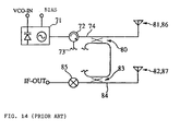
- Fig. 14 is an equivalent circuit diagram of the transmission and receiving apparatus shown in Fig. 13.
- the voltage-control oscillator 71 includes a varactor diode and a Gunn diode. An oscillation signal therefrom is propagated to the dielectric resonator 81 through the circulator 72 and radiated to the outside through a window formed in the conductor plate in the upper portion of the dielectric resonator 81 and the dielectric lens 86.
- the circulator 72 and the terminater 73 constitute an isolator.
- An RF signal received via the dielectric lens 87 and the dielectric resonator 82 is propagated through the dielectric strip 84.
- a Lo signal (local signal) is introduced to the dielectric strip 84 by the couplers 80 and 83 and input to the mixer 85.
- the mixer 85 is formed of a Schottky barrier diode and generates an IF signal (intermediate frequency signal).
- a curved line (bent portion) must be provided in a dielectric strip, and couplers comprising two dielectric strips which are brought close to each other must be provided at at least two places within the apparatus in order to supply a part of a transmission signal as a Lo signal (local signal) to the mixer.
- a large area is required to construct such a coupler.
- the orthogonality between the LSM01 mode and the LSE01 mode is distorted in the curved portion, and coupling occurs between the modes. Therefore, a low-loss characteristic of the line is realized only at the radius of curvature and the curved corner in a narrow range of the line.
- the shape of the coupler is limited, and formation of the apparatus into a small size is difficult.
- the aperture diameter of the antenna depends on the specifications of the transmission and receiving apparatus.
- the beam angle is 2°
- the antenna aperture diameter must be approximately 170 mm in the 60 GHz band.
- the beam width angle is 4°.
- the antenna aperture diameter must be approximately 90 mm.
- the transmission and receiving apparatus of Fig. 13 since the area where the coupler is formed together with the voltage-control oscillator and the mixer becomes larger than the antenna size, the transmission and receiving apparatus is forced to be enlarged as a whole.
- An object of the present invention is to provide a compact antenna-shared distributor and a transmission and receiving apparatus using such distributor.
- an antenna-shared distributor comprising: two facing conductor sections; and a dielectric resonator disposed between the conductor sections.
- a non-conductor section is provided in at least one of the conductor sections and at a position facing the dielectric resonator. Further, a first dielectric line and a second first dielectric line are disposed close to the dielectric resonator.
- this antenna-shared distributor is formed of only a resonator and at least two dielectric lines facing with each other with the resonator interposed in between, the antenna-shared distributor has a simple construction.
- a transmission and receiving apparatus comprising an oscillator coupled to one of the dielectric lines disposed with the antenna-shared distributor interposed therebetween, and a mixer circuit coupled to the other dielectric line.
- the transmission and receiving apparatus may further include an electromagnetic guide in the shape of a horn which is disposed around the non-conductor section.
- the horn makes it possible to efficiently focus radio waves onto the dielectric resonator.
- the transmission and receiving apparatus may further include a dielectric lens at a position facing the non-conductor section.
- the dielectric lens makes it possible to increase the focus of radio waves radiated from the dielectric resonator.
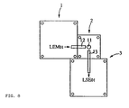
- a circuit unit 4 of Figs. 1A and 1B includes a voltage-control oscillator 1, an antenna-shared distributor 2, and a mixer 3.
- the antenna-shared distributor 2 is disposed in the center of the unit, and the voltage-control oscillator 1 and the mixer 3 are disposed on both sides of the antenna-shared distributor 2.
- the circuit unit 4, as shown in Fig. 1B, is mounted to the lower portion of a case 5 and is covered with a rear lid 6. Further, a dielectric lens 7 is mounted above the case 5.
- This dielectric lens 7 is made of a composite material of, for example, a resin and ceramic, with the specific inductive capacity thereof being set at approximately 4.0.
- a matching layer having a specific inductive capacity of approximately 2.0 for preventing reflection is provided on the top surface and the bottom surface of the dielectric lens 7.
- a dielectric resonator 11, serving as a primary vertical radiator, is provided at the focus position of the dielectric lens 7 in the center of the antenna-shared distributor 2.
- Figs. 2A and 2B are a top plan view and a sectional view of the antenna-shared distributor 2, respectively.
- An opening o is provided in the center of a conductor plate 14.
- the conductor plate 14 may be such that the surface of a conductor plate is coated with a conductor; in this case, in place of the opening o, a portion having the coating of the conductor removed may be provided.
- the dielectric resonator 11 which resonates in the HE111 mode is disposed below the opening o in such a manner for the axis of the dielectric resonator 11 to become normal to the main surface of the conductor plates 14 and 15.
- a first dielectric strip 12 and a second dielectric strip 13 are disposed between the conductor plates 14 and 15 in such a manner for the respective end portions of the dielectric strips 12 and 13 to face the dielectric resonator 11.
- the electromagnetic wave of the LSM mode in which an electric field having components at right angles to the direction of the length (in the x-axis direction in the figure) of the dielectric strip 12 and parallel (in the y-axis direction in the figure) to the conductor plates 14 and 15 and a magnetic field having components normal to the conductor plates 14 and 15 occur propagates within the dielectric strip 12.
- the dielectric resonator 11 Since the dielectric resonator 11 resonates in the HE111 mode having electric-field components in the same direction as that of the electric field of the dielectric strip 12, the first dielectric strip 12 and the dielectric resonator 11 are easily coupled to each other. Then, a linearly polarized electromagnetic wave is radiated in a direction normal (in the z-axis direction in the figure) to the conductor plate 14 via the opening o. Further, the dielectric line 13 formed of a dielectric strip and the dielectric resonator 11 are coupled to each other, and the electromagnetic wave propagates within the dielectric line 13 in the LSM mode, as shown in Fig. 2C. This signal is a Lo signal to be sent to the mixer 3 shown in Fig. 1A.
- an LSM01-mode signal propagates within the dielectric line 13 as a result of the coupling between the dielectric line 13 and the dielectric resonator 11.
- This signal is supplied as an RF signal to the mixer 3.
- the power distribution ratio of the radiation power of the transmission signal to the Lo signal may be set according to the spacing between the dielectric resonator 11 and the dielectric strips 12 and 13.
- Fig. 3 is an equivalent circuit diagram of the transmission and receiving apparatus shown in Figs. 1A and 1B.
- the voltage-control oscillator 1 includes a varactor diode and a Gunn diode.
- An oscillation signal Tx from the voltage-control oscillator 1 is distributed by the antenna-shared distributor 2 and is radiated from an antenna formed of the dielectric resonator and the dielectric lens 7 within the antenna-shared distributor.
- a part of the oscillation signal Tx is made to be a Lo signal and sent out to the mixer 3.
- a received signal RX is also distributed by the antenna-shared distributor 2, and one of the signals is supplied as an RF signal to the mixer 3.
- the mixer 3 outputs an IF signal.
- Fig. 4A is a sectional view of a dielectric line within the antenna-shared distributor, in which the dielectric strip 12 is fitted into the grooves formed in the conductor plates 14 and 15.
- Fig. 4B is a sectional view of a dielectric line within the voltage-control oscillator 1, in which similarly dielectric strips 16a and 16b are fitted into the grooves on the surface of the conductor plates 21 and 22, and a substrate 20 is disposed between the dielectric strips 16a and 16b.
- the cross section of the dielectric line within the mixer 3 is similar to that shown in Fig. 4B.
- an NRD guide can be constructed with the dielectric strip portion made as a propagation area and the other area made as a non-propagation area (cut-off area).
- Figs. 5A, 5B and 5C show the construction of the interior of the voltage-control oscillator 1 and the mixer 3.
- the dielectric strips 16a and 16b which connect to the dielectric strip 12 of the antenna-shared distributor 2 are provided, and an oscillation circuit 18 is provided on the substrate interposed between these two dielectric strips 16a and 16b.
- dielectric strips 17a and 17b which connect to the dielectric strip 13 of the antenna-shared distributor 2 are provided, and a mixer circuit 19 is formed on the substrate interposed between these two dielectric strips 17a and 17b.
- Fig. 5B is an enlarged view of the oscillation circuit 18.
- a suspended line 25 extends in a direction normal to the dielectric strips 16a and 16b, and a conductor pattern 26 for RF choke and further electrodes 23 and 24 are connected to the end of the suspended line 25.
- One pole of a Gunn diode 27 is connected to the suspended line 25.
- a varactor diode 28 is connected between the conductor pattern 26 for RF choke and the suspended line 25.
- the other pole of the Gunn diode 27 is grounded, and the application of a bias voltage to the Gunn diode between the electrode 23 and the ground causes the Gunn diode to oscillate. Since the conductor pattern 26 for RF choke can be assumed to be grounded in a high frequency region, the varactor diode 28 is connected equivalently in parallel to the Gunn diode 27.
- a modulation signal applied between the electrodes 23 and 24 causes the electrostatic capacity of the varactor diode to change, causing the oscillation frequency of the Gunn diode to be modulated.
- Fig. 5C is an enlarged view of the mixer circuit 19.
- the conductor patterns 26 for RF choke extend in a direction normal to the dielectric strips 17a and 17b, and electrodes 29 and 30 are formed in the end portions of the conductor patterns 26.
- a Schottky barrier diode 31 is mounted in that portion between the end portions of the two conductor patterns for RF choke which is interposed between the dielectric strips 17a and 17b.
- the Schottky barrier diode 31 is coupled to an RF signal and an Lo signal which are propagated through the dielectric strips 17a and 17b and generates an IF signal when a bias voltage is applied between the electrodes 29 and 30.
- Figs. 6A, 6B and 6C show two other construction examples of the antenna-shared distributor.
- a dielectric rod 40 which goes through the conductor plate 14 and connects to the dielectric resonator 11, such as that shown in Fig. 6A, may be provided.
- This dielectric rod 40 functions as a dielectric rod antenna, making it possible to increase the directivity of the antenna.
- a plate 41 having a slot may be disposed between the dielectric resonator 11 and the conductor plate 14.
- the plate 41 may be such that an opening of any desired pattern is formed within a metallic plate or any desired pattern is formed by removing a part of a conductor plate on the circuit substrate. Varying the slot arrangement pattern makes it possible to control the directivity of radio waves from the antenna.
- Fig. 7A shows the internal construction of a transmission and receiving apparatus according to a second embodiment of the present invention.
- An oscillation signal from an oscillation circuit 38 is supplied to the antenna-shared distributor 2 via a circulator 42.
- a signal from the antenna-shared distributor 2 to a voltage-control oscillator 100 is supplied to a terminater 43 via the circulator 42.
- the isolator 42 and the voltage-control oscillator 100 are different modules.
- all of an isolator 42', a terminater 43', and an oscillation circuit 18' may be housed inside a voltage-control oscillator 150.
- Fig. 8 shows the interior construction of a transmission and receiving apparatus according to a third embodiment of the present invention.
- the dielectric strips 12 and 13 are made to intersect at right angles to each other.
- the dielectric resonator 11 excites in the HE111 mode and radiates a linearly polarized electromagnetic wave in the forward direction of Fig. 8, and at the same time radiates a signal of the LSE01 mode to the dielectric strip 13.
- This LSE01-mode signal becomes a Lo signal to the mixer 3.
- a reflection signal from the target object is made to enter the dielectric resonator 11 and an RF signal therefrom is supplied to the mixer 3 in the LSE01 mode.
- the power distribution ratio of the radiation power of the transmission signal to the Lo signal may be set according to the spacing between the dielectric resonator 11 and the dielectric strips 12 and 13.
- Fig. 9A is a sectional view of a transmission and receiving apparatus according to a fourth embodiment of the present invention.
- a part of the case 5 extends up to near the dielectric resonator 11.
- a opening portion H is formed above the dielectric resonator 11 in the extension portion of the case 5.
- the slope of the extension portion in which the opening portion H is formed forms the horn.
- the circuit unit 4 may be disposed within the case 5.
- a dielectric lens formed of a lamination of dielectric layers 61a to 61n having mutually different specific inductive capacity and a dielectric convex lens element 60 may be used. In this case, by decreasing the specific inductive capacity in such a way that the specific inductive capacity becomes smaller gradually from the topmost dielectric layer 61a to the bottommost dielectric layer 61n, the dielectric lens can be made thin.
- Figs. 10A1 and 10A2 show another dielectric line for use in a transmission and receiving apparatus of the present invention.
- a normal-type dielectric line 500 in which grooves are not formed in the upper and lower conductor plates may be used in an antenna-shared distributor.
- a dielectric line with a circuit substrate 506 interposed in the middle thereof may be used in the voltage-control oscillator and the mixer.
- a wing-type dielectric line such that wings 503' and 504' extend to the right and left in the figures from dielectric lines 503 and 504 may be used.
- the wing-type dielectric lines 503 and 504 with the circuit substrate 506 interposed therebetween may be used.
- the compact and simple antenna-shared distributor and the transmission and receiving apparatus using such distributor according to the present invention makes it possible to save space when they are mounted in a vehicle. Further, the simple construction increases fault tolerance.
Landscapes
- Engineering & Computer Science (AREA)
- Radar, Positioning & Navigation (AREA)
- Remote Sensing (AREA)
- Computer Security & Cryptography (AREA)
- Physics & Mathematics (AREA)
- General Physics & Mathematics (AREA)
- Computer Networks & Wireless Communication (AREA)
- Radar Systems Or Details Thereof (AREA)
- Aerials With Secondary Devices (AREA)
- Waveguides (AREA)
- Waveguide Aerials (AREA)
- Details Of Aerials (AREA)
- Transceivers (AREA)
- Control Of Motors That Do Not Use Commutators (AREA)
Abstract
Description
Claims (17)
- An antenna-shared distributor, comprising:two facing conductor sections (14, 15);a dielectric resonator (11) disposed between said conductor sections (14, 15);a non-conductor section which is provided in at least one of said conductor sections (14, 15) and which faces said dielectric resonator (11);a first dielectric line (12) disposed close to said dielectric resonator (11); anda second dielectric line (13) disposed close to said dielectric resonator (11).
- An antenna-shared distributor according to claim 1, wherein said non-conductor section is a hole (o) which goes through the conductor section (14).
- An antenna-shared distributor according to claim 1, further comprising: grooves which are provided in said conductor section and which hold said dielectric line.
- An antenna-shared distributor according to claim 1, further comprising: a dielectric wing section which extends along the surface of said facing conductor section from said dielectric line.
- An antenna-shared distributor according to claim 1, further comprising: a dielectric rod (40) which couples electromagnetically to said dielectric resonator (11).
- An antenna-shared distributor according to claim 5, wherein said dielectric rod (40) goes through said non-conductor section (o).
- An antenna-shared distributor according to claim 1, wherein said non-conductor section is a slot provided in said non-conductor section.
- A transmission and receiving apparatus, comprising:an antenna-shared distributor (2) including:two facing conductor sections (14, 15);a dielectric resonator (11) disposed between said conductor sections (14, 15);a non-conductor section which is provided in at least one of said conductor sections and which faces said dielectric resonator (11);a first dielectric line (12) disposed close to said dielectric resonator (11); anda second dielectric line (13) disposed close to said dielectric resonator (11);an oscillator (1; 100; 150) coupled to said first dielectric line (12); anda mixer (3) coupled to said second dielectric line (13).
- A transmission and receiving apparatus according to claim 8,
wherein said oscillator (1) includes:a third dielectric line (16a, 16b) coupled to said dielectric resonator (11); andan oscillator (18) coupled to said third dielectric line (16a, 16b). - A transmission and receiving apparatus according to claim 9,
wherein said oscillator includes:a suspended line (25) coupled to said third dielectric line (16a, 16b);an RF choke (26) connected to said suspended line (25); andelectrodes (23, 24) connected to said RF choke (26). - A transmission and receiving apparatus according to claim 8,
wherein said mixer (3) includes: a fourth dielectric line (17a, 17b) coupled to said dielectric resonator (11); anda mixer circuit (19) coupled to said fourth dielectric line (17a, 17b). - A transmission and receiving apparatus according to claim 11,
wherein said mixer circuit includes:a switching element (31) coupled to said fourth dielectric line (17a, 17b);an RF choke (26) connected to said switching element (31); andelectrodes (29, 30) connected to said RF choke (26). - A transmission and receiving apparatus according to claim 8, further comprising: a horn-shaped electromagnetic guide (H) disposed around said non-conductor section.
- A transmission and receiving apparatus according to claim 9,
wherein said oscillator includes:a circulator (42) having three terminals, inserted in the middle of said third dielectric line (16a, 16b), two terminals of which are coupled to said third dielectric line (16a, 16b); anda terminater (43) connected to the rest terminals of said circulator (42). - A transmission and receiving apparatus according to claim 8, wherein said first dielectric line (12), said second dielectric line (13) and said dielectric resonator (11) are provided in line with each other.
- A transmission and receiving apparatus according to claim 8, wherein the line which connects the extension line of said dielectric resonator (11) and said first dielectric line (12) substantially intersects at right angles to the line which connects the extension line of said dielectric resonator (11) and said second dielectric line (13).
- A transmission and receiving apparatus according to claim 8, further comprising: a dielectric lens (7) at a position facing said non-conductor section.
Applications Claiming Priority (3)
| Application Number | Priority Date | Filing Date | Title |
|---|---|---|---|
| JP08280681A JP3119176B2 (en) | 1996-10-23 | 1996-10-23 | Antenna shared distributor and transmitter / receiver for dielectric line |
| JP280681/96 | 1996-10-23 | ||
| JP28068196 | 1996-10-23 |
Publications (2)
| Publication Number | Publication Date |
|---|---|
| EP0838693A1 true EP0838693A1 (en) | 1998-04-29 |
| EP0838693B1 EP0838693B1 (en) | 2001-04-25 |
Family
ID=17628458
Family Applications (1)
| Application Number | Title | Priority Date | Filing Date |
|---|---|---|---|
| EP97118293A Expired - Lifetime EP0838693B1 (en) | 1996-10-23 | 1997-10-21 | Antenna-shared distributor and transmission and receiving apparatus using same |
Country Status (5)
| Country | Link |
|---|---|
| US (1) | US6008755A (en) |
| EP (1) | EP0838693B1 (en) |
| JP (1) | JP3119176B2 (en) |
| CN (1) | CN1116616C (en) |
| DE (1) | DE69704649T2 (en) |
Cited By (5)
| Publication number | Priority date | Publication date | Assignee | Title |
|---|---|---|---|---|
| EP0855755A3 (en) * | 1997-01-23 | 2000-05-31 | Murata Manufacturing Co., Ltd. | Dielectric line intersection |
| EP0969548A3 (en) * | 1998-07-03 | 2001-03-28 | Murata Manufacturing Co., Ltd. | Antenna device, and transmitting/receiving unit |
| EP0971436A3 (en) * | 1998-07-06 | 2001-11-07 | Murata Manufacturing Co., Ltd. | Antenna device and transmitting/receiving apparatus |
| EP1674882A1 (en) * | 2004-12-27 | 2006-06-28 | TDK Corporation | Radar device |
| EP3336575A1 (en) * | 2016-11-18 | 2018-06-20 | Valeo Schalter und Sensoren GmbH | Radar sensor for a motor vehicle with an antenna element embedded in a radome, driver assistance system and motor vehicle |
Families Citing this family (26)
| Publication number | Priority date | Publication date | Assignee | Title |
|---|---|---|---|---|
| US6073052A (en) * | 1996-11-15 | 2000-06-06 | Zelickson; Brian D. | Device and method for treatment of gastroesophageal reflux disease |
| JP3303757B2 (en) * | 1997-12-25 | 2002-07-22 | 株式会社村田製作所 | Non-radiative dielectric line component and integrated circuit thereof |
| JP3422268B2 (en) * | 1998-12-02 | 2003-06-30 | 株式会社村田製作所 | Dielectric lens antenna and wireless device using the same |
| DE19963625A1 (en) * | 1999-12-29 | 2001-07-12 | Bosch Gmbh Robert | Procedure for measuring the distance and speed of objects |
| JP2002246832A (en) * | 2001-02-15 | 2002-08-30 | Matsushita Electric Ind Co Ltd | Communication device |
| JP3700617B2 (en) * | 2001-07-04 | 2005-09-28 | 株式会社村田製作所 | Lens antenna |
| JP2003101301A (en) * | 2001-09-19 | 2003-04-04 | Murata Mfg Co Ltd | High-frequency module, communication device, and radar device |
| US20050024262A1 (en) | 2003-08-01 | 2005-02-03 | Ben Cantrell | Simultaneous transmission of multiple signals through a common shared aperture |
| DE102005008733A1 (en) * | 2004-02-26 | 2005-10-13 | Kyocera Corp. | Transceiver antenna, isolator, high frequency oscillator and the same high frequency transmitter / receiver |
| CN100435414C (en) * | 2006-01-23 | 2008-11-19 | 京信通信技术(广州)有限公司 | Differential Phase Continuously Variable Beamforming Network |
| DE102007034329A1 (en) * | 2007-07-24 | 2009-01-29 | Robert Bosch Gmbh | radar device |
| DE102012202913B4 (en) * | 2012-02-27 | 2026-02-05 | Robert Bosch Gmbh | radar sensor |
| JP2014155098A (en) * | 2013-02-12 | 2014-08-25 | Nitto Denko Corp | Antenna module and method for manufacturing the same |
| CN104270164B (en) * | 2014-09-24 | 2016-08-24 | 重庆长安汽车股份有限公司 | A kind of seat radio and transmitter receiver common antenna |
| EP3613150A4 (en) * | 2017-04-20 | 2020-12-02 | The Board of Trustees of the Leland Stanford Junior University | SCALABLE MM WAVE ARRAYS WITH LARGE APERTURES THAT ARE REALIZED BY MM WAVE DIELECTRIC WAVE CONDUCTORS |
| US11283189B2 (en) | 2017-05-02 | 2022-03-22 | Rogers Corporation | Connected dielectric resonator antenna array and method of making the same |
| KR102312067B1 (en) * | 2017-06-07 | 2021-10-13 | 로저스코포레이션 | Dielectric Resonator Antenna System |
| US11616302B2 (en) | 2018-01-15 | 2023-03-28 | Rogers Corporation | Dielectric resonator antenna having first and second dielectric portions |
| US11552390B2 (en) | 2018-09-11 | 2023-01-10 | Rogers Corporation | Dielectric resonator antenna system |
| US11016574B2 (en) | 2018-10-31 | 2021-05-25 | Rogers Corporation | Millimeter-wave-radar-based electromagnetic apparatus |
| JP6759309B2 (en) * | 2018-12-03 | 2020-09-23 | 日立オートモティブシステムズ株式会社 | Sensor with flat beam generating antenna |
| CN113169455A (en) | 2018-12-04 | 2021-07-23 | 罗杰斯公司 | Dielectric electromagnetic structure and method of manufacturing the same |
| US12216191B2 (en) | 2019-04-01 | 2025-02-04 | Richwave Technology Corp. | Methods, circuits, and apparatus for motion detection, doppler shift detection, and positioning by self-envelope modulation |
| CN110109082A (en) * | 2019-04-17 | 2019-08-09 | 天津大学 | A kind of Terahertz Active Radar imaging array of shared antenna |
| US11482790B2 (en) | 2020-04-08 | 2022-10-25 | Rogers Corporation | Dielectric lens and electromagnetic device with same |
| CN111585050B (en) * | 2020-05-18 | 2021-03-02 | 宁波大学 | A Broadband Flat Panel Array Antenna |
Citations (7)
| Publication number | Priority date | Publication date | Assignee | Title |
|---|---|---|---|---|
| US4731611A (en) * | 1983-06-21 | 1988-03-15 | Siemens Aktiengesellschaft | Stripline doppler radar |
| JPH0794915A (en) * | 1993-09-17 | 1995-04-07 | Nippon Valqua Ind Ltd | NRD guide circuit and manufacturing method thereof |
| JPH07131235A (en) * | 1993-11-05 | 1995-05-19 | Mitsui Eng & Shipbuild Co Ltd | Slot antenna with dielectric resonator |
| US5497163A (en) * | 1993-08-09 | 1996-03-05 | Siemens Aktiengesellschaft | Doppler radar module using micro-stripline technology |
| EP0700114A2 (en) * | 1994-08-30 | 1996-03-06 | Murata Manufacturing Co., Ltd. | High-frequency integrated circuit |
| EP0709912A1 (en) * | 1994-10-25 | 1996-05-01 | Honda Giken Kogyo Kabushiki Kaisha | NRD guide circuit, radar module and radar apparatus |
| EP0743697A1 (en) * | 1995-05-19 | 1996-11-20 | Murata Manufacturing Co., Ltd. | Dielectric antenna |
Family Cites Families (2)
| Publication number | Priority date | Publication date | Assignee | Title |
|---|---|---|---|---|
| US4789844A (en) * | 1987-05-29 | 1988-12-06 | Raytheon Company | Broad-band non-reciprocal microwave devices |
| JP3230353B2 (en) * | 1993-11-18 | 2001-11-19 | 株式会社村田製作所 | Antenna duplexer |
-
1996
- 1996-10-23 JP JP08280681A patent/JP3119176B2/en not_active Expired - Fee Related
-
1997
- 1997-10-21 EP EP97118293A patent/EP0838693B1/en not_active Expired - Lifetime
- 1997-10-21 DE DE69704649T patent/DE69704649T2/en not_active Expired - Fee Related
- 1997-10-22 US US08/956,212 patent/US6008755A/en not_active Expired - Fee Related
- 1997-10-23 CN CN97125265A patent/CN1116616C/en not_active Expired - Fee Related
Patent Citations (7)
| Publication number | Priority date | Publication date | Assignee | Title |
|---|---|---|---|---|
| US4731611A (en) * | 1983-06-21 | 1988-03-15 | Siemens Aktiengesellschaft | Stripline doppler radar |
| US5497163A (en) * | 1993-08-09 | 1996-03-05 | Siemens Aktiengesellschaft | Doppler radar module using micro-stripline technology |
| JPH0794915A (en) * | 1993-09-17 | 1995-04-07 | Nippon Valqua Ind Ltd | NRD guide circuit and manufacturing method thereof |
| JPH07131235A (en) * | 1993-11-05 | 1995-05-19 | Mitsui Eng & Shipbuild Co Ltd | Slot antenna with dielectric resonator |
| EP0700114A2 (en) * | 1994-08-30 | 1996-03-06 | Murata Manufacturing Co., Ltd. | High-frequency integrated circuit |
| EP0709912A1 (en) * | 1994-10-25 | 1996-05-01 | Honda Giken Kogyo Kabushiki Kaisha | NRD guide circuit, radar module and radar apparatus |
| EP0743697A1 (en) * | 1995-05-19 | 1996-11-20 | Murata Manufacturing Co., Ltd. | Dielectric antenna |
Non-Patent Citations (2)
| Title |
|---|
| PATENT ABSTRACTS OF JAPAN vol. 095, no. 007 31 August 1995 (1995-08-31) * |
| PATENT ABSTRACTS OF JAPAN vol. 095, no. 008 29 September 1995 (1995-09-29) * |
Cited By (5)
| Publication number | Priority date | Publication date | Assignee | Title |
|---|---|---|---|---|
| EP0855755A3 (en) * | 1997-01-23 | 2000-05-31 | Murata Manufacturing Co., Ltd. | Dielectric line intersection |
| EP0969548A3 (en) * | 1998-07-03 | 2001-03-28 | Murata Manufacturing Co., Ltd. | Antenna device, and transmitting/receiving unit |
| EP0971436A3 (en) * | 1998-07-06 | 2001-11-07 | Murata Manufacturing Co., Ltd. | Antenna device and transmitting/receiving apparatus |
| EP1674882A1 (en) * | 2004-12-27 | 2006-06-28 | TDK Corporation | Radar device |
| EP3336575A1 (en) * | 2016-11-18 | 2018-06-20 | Valeo Schalter und Sensoren GmbH | Radar sensor for a motor vehicle with an antenna element embedded in a radome, driver assistance system and motor vehicle |
Also Published As
| Publication number | Publication date |
|---|---|
| DE69704649D1 (en) | 2001-05-31 |
| EP0838693B1 (en) | 2001-04-25 |
| US6008755A (en) | 1999-12-28 |
| DE69704649T2 (en) | 2002-04-18 |
| CN1189705A (en) | 1998-08-05 |
| JP3119176B2 (en) | 2000-12-18 |
| CN1116616C (en) | 2003-07-30 |
| JPH10126109A (en) | 1998-05-15 |
Similar Documents
| Publication | Publication Date | Title |
|---|---|---|
| US6008755A (en) | Antenna-shared distributor and transmission and receiving apparatus using same | |
| EP0817394B1 (en) | Transmitter-receiver | |
| EP0871239B1 (en) | Antenna device and radar module | |
| US6362795B2 (en) | Antenna apparatus and transmission and receiving apparatus using the same | |
| US6868258B2 (en) | Structure for connecting non-radiative dielectric waveguide and metal waveguide, millimeter wave transmitting/receiving module and millimeter wave transmitter/receiver | |
| JPH08191211A (en) | Antenna | |
| JP3259637B2 (en) | Transceiver | |
| US6342863B2 (en) | Antenna apparatus and antenna and tranceiver using the same | |
| JP3743093B2 (en) | Transceiver | |
| JP2922741B2 (en) | Radar module | |
| JP3259021B2 (en) | Radar module | |
| JP2002076721A (en) | Connection structure between non-radiative dielectric line and metal waveguide, millimeter wave transceiver, and millimeter wave transceiver | |
| JP2002016406A (en) | Connection structure between non-radiative dielectric line and metal waveguide, millimeter wave transceiver, and millimeter wave transceiver | |
| JP2002135056A (en) | High frequency diode oscillator and millimeter wave transceiver using the same | |
| JP2002043656A (en) | High frequency diode oscillator and millimeter wave transceiver using the same | |
| JPH06214008A (en) | Nonradiating dielectric line radar module | |
| JPH07209409A (en) | Radar module | |
| JP2002299920A (en) | Connection structure between nonradiative dielectric line and metal waveguide and millimeter wave transceiver | |
| JP2003198218A (en) | Connection structure between nonradiative dielectric line and metal waveguide and millimeter wave transceiver | |
| JP2001237645A (en) | High frequency diode oscillator and millimeter wave transceiver using the same |
Legal Events
| Date | Code | Title | Description |
|---|---|---|---|
| PUAI | Public reference made under article 153(3) epc to a published international application that has entered the european phase |
Free format text: ORIGINAL CODE: 0009012 |
|
| 17P | Request for examination filed |
Effective date: 19971021 |
|
| AK | Designated contracting states |
Kind code of ref document: A1 Designated state(s): DE FR GB |
|
| AX | Request for extension of the european patent |
Free format text: AL;LT;LV;RO;SI |
|
| AKX | Designation fees paid |
Free format text: DE FR GB |
|
| RBV | Designated contracting states (corrected) |
Designated state(s): DE FR GB |
|
| 17Q | First examination report despatched |
Effective date: 19990616 |
|
| GRAG | Despatch of communication of intention to grant |
Free format text: ORIGINAL CODE: EPIDOS AGRA |
|
| GRAG | Despatch of communication of intention to grant |
Free format text: ORIGINAL CODE: EPIDOS AGRA |
|
| GRAH | Despatch of communication of intention to grant a patent |
Free format text: ORIGINAL CODE: EPIDOS IGRA |
|
| GRAH | Despatch of communication of intention to grant a patent |
Free format text: ORIGINAL CODE: EPIDOS IGRA |
|
| GRAA | (expected) grant |
Free format text: ORIGINAL CODE: 0009210 |
|
| AK | Designated contracting states |
Kind code of ref document: B1 Designated state(s): DE FR GB |
|
| REF | Corresponds to: |
Ref document number: 69704649 Country of ref document: DE Date of ref document: 20010531 |
|
| ET | Fr: translation filed | ||
| REG | Reference to a national code |
Ref country code: GB Ref legal event code: IF02 |
|
| PLBE | No opposition filed within time limit |
Free format text: ORIGINAL CODE: 0009261 |
|
| STAA | Information on the status of an ep patent application or granted ep patent |
Free format text: STATUS: NO OPPOSITION FILED WITHIN TIME LIMIT |
|
| 26N | No opposition filed | ||
| PGFP | Annual fee paid to national office [announced via postgrant information from national office to epo] |
Ref country code: DE Payment date: 20081016 Year of fee payment: 12 |
|
| PGFP | Annual fee paid to national office [announced via postgrant information from national office to epo] |
Ref country code: FR Payment date: 20081014 Year of fee payment: 12 |
|
| PGFP | Annual fee paid to national office [announced via postgrant information from national office to epo] |
Ref country code: GB Payment date: 20081015 Year of fee payment: 12 |
|
| REG | Reference to a national code |
Ref country code: FR Ref legal event code: ST Effective date: 20100630 |
|
| PG25 | Lapsed in a contracting state [announced via postgrant information from national office to epo] |
Ref country code: FR Free format text: LAPSE BECAUSE OF NON-PAYMENT OF DUE FEES Effective date: 20091102 Ref country code: DE Free format text: LAPSE BECAUSE OF NON-PAYMENT OF DUE FEES Effective date: 20100501 |
|
| PG25 | Lapsed in a contracting state [announced via postgrant information from national office to epo] |
Ref country code: GB Free format text: LAPSE BECAUSE OF NON-PAYMENT OF DUE FEES Effective date: 20091021 |