EP0848333B1 - Méthode et dispositif pour logique de terminaison dynamique de bus de données - Google Patents
Méthode et dispositif pour logique de terminaison dynamique de bus de données Download PDFInfo
- Publication number
- EP0848333B1 EP0848333B1 EP97309919A EP97309919A EP0848333B1 EP 0848333 B1 EP0848333 B1 EP 0848333B1 EP 97309919 A EP97309919 A EP 97309919A EP 97309919 A EP97309919 A EP 97309919A EP 0848333 B1 EP0848333 B1 EP 0848333B1
- Authority
- EP
- European Patent Office
- Prior art keywords
- data bus
- driver
- mid
- transistor
- signal
- Prior art date
- Legal status (The legal status is an assumption and is not a legal conclusion. Google has not performed a legal analysis and makes no representation as to the accuracy of the status listed.)
- Expired - Lifetime
Links
Images


Classifications
-
- G—PHYSICS
- G06—COMPUTING OR CALCULATING; COUNTING
- G06F—ELECTRIC DIGITAL DATA PROCESSING
- G06F13/00—Interconnection of, or transfer of information or other signals between, memories, input/output devices or central processing units
- G06F13/38—Information transfer, e.g. on bus
- G06F13/40—Bus structure
- G06F13/4063—Device-to-bus coupling
- G06F13/4068—Electrical coupling
- G06F13/4086—Bus impedance matching, e.g. termination
Definitions
- the present invention relates to data bus transfers and more particularly to dynamic termination logic of data buses to improve performance of the data buses.
- the data bus provides transfers of data in the form of electrical signals from one subsystem to another. Often times the data bus of a system gets overwhelmed with data transfers and becomes the bottle neck of the system.
- a typical bi-directional bus design has at least two end-drivers, each located to one end of the bi-directional data bus and is configured for wire-oring of data signals on the data bus. In the wire-or configuration, either end-driver is able to drive data signals on the data bus. When the end-drivers are inactive, the data bus is pulled-up to a logic high state, "1". When an end-driver is active and driving the data bus, the data bus is at the logic low level, "0".
- switching wave signals are generated. If the switching wave signals are not terminated, reflections of the switching wave signals occur that will cause ringing on the data bus.
- the ringing causes the data signals on the data bus to be unsettled.
- An unsettled data bus produces unstable data.
- Ringing on the data bus is undesirable because the ringing reduces the speed at which data signals are transferred on the data bus. Time wasted waiting for the data bus to settle from the ringing can be best used for additional data transfers.
- Present data bus designs attach a termination resistor at each of the data bus to terminate the switching wave signals.
- the termination resistors serve a dual purpose of terminating the switching wave signal and providing a pull-up signal to produce a logic high state on the data bus when the end-drivers are inactive.
- the end-drivers are typically open drain or open collector transistors depending on whether the transistors are formed using CMOS (complementary metal oxide silicon) or bipolar processes.
- CMOS complementary metal oxide silicon
- a negative switching wave signal (transition from an initial high logic state to a low logic state) generated from the active end-driver travels to the end of the data bus and is terminated without reflections by the termination resistor at the end of the data bus.
- back to back switching occurs with the end-drivers.
- Back to back switching occurs when both end-drivers are simultaneously switching between active and inactive states of operation.
- a negative switching wave signal (transition from a high logic state to a low logic state) is generated.
- a positive switching wave signal transition from a low logic state to a high logic state
- the negative switching wave signal terminates when it reaches the termination resistor at the end of the data bus, but the positive switching wave signal produces a reflection from the active end-driver which has a resistance other than the characteristic impedance of the data bus.
- a wire-or glitch results from the reflection of the positive switching wave signal. The wire-or glitch causes ringing on the data bus and produces unsettled data signals on the data bus. Time is wasted waiting for the ringing on the data bus to settle.
- the data buses are often formed as traces on printed circuit boards which route the data buses to the various circuit components of a subsystem.
- the printed circuit boards of a computer may include tens of data buses coupling the multitude of the circuit components together.
- US 5311081 discloses a data bus that uses open drain drivers and differential receivers together with distributed termination impedances. Each module connected to the bus contains a termination impedance located on that module. The termination impedance is chosen so that a minimum settling time is achieved, both when a particular driver is active, as well as when drivers on two different modules are active.
- US 5165046 discloses a high speed CMOS driver circuit which compensates for intervening transmission line effects, for example caused by the presence of a printed circuit board, or on a silicon substrate between coupled CMOS devices.
- a bi-directional data bus for wire-or data transfers comprises a first end-driver coupled to a first end of the data bus configured to drive the first end of the data bus with a first signal.
- a second end-driver coupled to the second end of the data bus is configured to dynamically terminate the first signal from the first end-driver.
- a mid-driver is also coupled to the data bus. The impedance of the mid-driver is half the characteristic impedance of the data bus.
- the first end-driver includes a pull-up transistor with a resistive value of the characteristic impedance of the data bus and a pull-down transistor with a resistive value of the characteristic impedance of the data bus.
- the second end-driver includes a pull-up transistor with a resistive value of the characteristic impedance of the data bus and a pull-down transistor with a resistive value of the characteristic impedance of the data bus.
- the termination resistors are integrated with the second end-driver and act to terminate the first signal. Thus, regardless of the state of the second end-driver being active or inactive, a resistive value of the characteristic impedance is coupled to the data bus to terminate the first signal from the first end-driver.
- the second end-driver drives the data bus with a second signal and the first end-driver dynamically terminates the second signal from the second end-driver.
- the termination resistors are integrated with the first end-driver.
- the first end-driver and the second end-driver simultaneously dynamically terminate the first and the second signals.
- the received first signal at the second end-driver and the received second signal at the first end-driver dynamically terminate with the characteristic impedance of the data bus upon reaching the end-drivers.
- the characteristic impedance of the data bus is coupled to the data bus for proper termination to prevent reflections and thus, settles the data bus to allow other data signals to drive the data bus sooner rather than waiting for reflections from a switching wave signal to settle.
- a first mid-driver coupled to the data bus is configured to drive the data bus with a third signal
- a second mid-driver coupled to the data bus is configured to drive the data bus with a fourth signal.
- the second end-driver dynamically terminates a reflection of the fourth signal from the first mid-driver
- the first end-driver dynamically terminates a reflection of the third signal from the second mid-driver.
- An apparatus and method for operating an improved data bus are provided by the dynamic termination logic to terminate data signals on the data bus for improved data bus settling times.
- Integration of the termination resistors for the data bus with the drivers eliminates the need for external placement of the termination resistors to the printed circuit boards or the like of a computer system. Space savings from eliminating the external resistors affords more space on the printed circuit boards for additional circuit components and circuitry that further enables integration of more functions in even smaller packages.
- reducing settling time of the data bus affords data bus designs with increased data rates. Increasing the data rates of a computer subsystem increases the speed at which an overall system processes data.
- the dynamic termination logic not only increases available space on a printed circuit board but also increases the throughput of a system for performing data transfers.
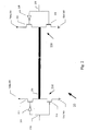
- Fig. 1 generally shows a system of a computer network 10.
- the computer network 10 includes a client 110, a client 120, a client 130, a client 140, and an Internet 150.
- the Internet 150 couples the clients 110, 120, 130, and 140 enables communication between the clients.
- the Internet 150 provides TCP/IP (Transmission Control Protocol over Internet Protocol).
- TCP/IP Transmission Control Protocol over Internet Protocol
- Other represented segments operating the TCP/IP including intranets and local area networks are also suitable.
- Bi-directional data buses 115, 125, 135, and 145 provide dynamic termination logic for improved data bus performance.
- the data buses 115, 125, 135, and 145 provide network connections between the clients 110, 120, 130, and 140 and the Internet 150.
- Data bus 115 provides a network connection for the client 110 to access the Internet 150.
- Data bus 125 provides a network connection for the client 120 to access the Internet 150.
- Data bus 135 provides a network connection for the client 130 to access the Internet 150.
- Data bus 145 provides a network connection for the client 140 to access to the Internet 150.
- the clients 110, 120, 130, and 140 include logic circuits that are programmed to perform a series of specifically identified operations for data transfers to and from the Internet 150.
- the data buses 115, 125, 135, and 145 include logic circuits that provide dynamic termination logic of the data buses.
- data transfers between the client 110 and the client 120 occur via the data bus 115, to the Internet 150, to the data bus 125, and to the client 120.
- data transfers between the client 120 and the client 110 occur via the data bus 125, to the Internet 150, to the data bus 115, and to the client 110.
- data transfers between the clients include coupling a data bus between two clients to facilitate the data transfers.
- a simpler computer network provides data transfers between two clients via a dynamically terminated data bus.
- the clients 110, 120, 130, and 140 include dynamically terminated data buses in accordance with the present invention to facilitate the internal data transfers.
- the data buses having dynamically terminated logic are included throughout the computer network 10.
- Fig. 2 shows a circuit diagram of a dynamic termination logic data bus 20 in in accordance with the invention.
- the dynamic termination logic data bus 20 includes an end-driver 210, an end-driver 220, and a data bus 250 set in a wire-or configuration.
- the end-driver 210 is coupled to the data bus 250 and provides drive outputs to the data bus 250.
- the end-driver 220 is coupled to the data bus 250 and provides drive outputs to the data bus 250.
- the drive outputs from the end-drivers 210 and 220 provide switching waves between Vddq voltage and 1/2 Vddq voltage.
- Vddq voltage and the 1/2 Vddq voltage represent a high logic state, "1" and a low logic state, "0" on the data bus 250, respectively.
- MOS transistors are shown, other variations of transistors may be used.
- the drivers perform switching functions, other devices that facilitate switching functions may be substituted for the transistors.
- the end-driver 210 includes a MOS (Metal Oxide Silicon) transistor 212, a MOS transistor 214, control input 216, and an invertor 218.
- Drain of transistor 212 is coupled to Vddq 255, and source of transistor 212 is coupled to the data bus 250 and drain of the transistor 214.
- Source of transistor 214 is coupled to Gnd 265.
- the output of invertor 218 is coupled to the gate of transistor 212.
- Control input 216 coupled to the input of the invertor 218 and the gate of transistor 214 provides control signals to activate the end-driver 210.
- transistor 212 and transistor 214 can be implemented in CMOS (complementary MOS) so that the transistor 212 and invertor 218 become a p-channel transistor and the transistor 214 a n-channel transistor.
- CMOS complementary MOS
- the end-driver 220 includes a MOS transistor 222, a MOS transistor 224, control input 226, and invertor 228. Drain of transistor 222 is coupled to Vddq 255, and source of transistor 222 is coupled to the data bus 250 and drain of the transistor 224. Source of transistor 224 is coupled to Gnd 265. The output of the invertor 228 is coupled to the gate of transistor 222. Control input 226 coupled to the input of the invertor 228 and the gate of transistor 224 provides control signals to activate the end-driver 220.
- the transistor 222 and invertor 228 become a p-channel transistor and the transistor 224 a n-channel transistor in CMOS implementation.
- the transistors of the end-drivers 210 and 220 are formed to provide a resistance set to the characteristic impedance of the data bus 250.
- the resistance of the activated transistors match the characteristic impedance of the data bus 250.
- Switching signal waves received at the end-drivers are terminated with the characteristic impedance of the data bus.
- the embodiment of the invention provides that the characteristic impedance of the data bus 250 to be 50 ⁇ (ohms) which sets the resistance of an activated transistor of an end-driver to be also 50 ⁇ .
- the dynamic termination logic data bus 20 terminates the switching signal waves from the end-drivers to prevent reflections onto the data bus 250.
- end-driver 210 is initially inactive.
- the control input 216 provides an input that turns-on transistor 212 and turns-off transistor 214 which couples Vddq 255 to the data bus 250 via transistor 212.
- End-driver 220 is initially active.
- the control input 226 provides an input that turns-off transistor 222 and turns-on transistor 224 which couples the data bus 250 to Gnd 265 via transistor 224.
- the initial state of the data bus 250 is at a 1/2 Vddq voltage which corresponds to a low logic state.
- control input 216 provides an input that activates end-driver 210
- control input 226 provides an input that deactivates end-driver 220.
- transistor 212 turns-off and transistor 214 turns-on generating a negative switching wave signal of 1/2 Vddq voltage to Gnd voltage.
- transistor 222 turns-on and transistor 224 turns-off generating a positive switching wave signal of 1/2 Vddq voltage to Vddq voltage.
- each switching wave signal terminates at the end of the data bus 250 with the end-driver.
- the end-driver 220 receives the negative switching wave signal from the end-driver 210 and terminates the negative switching wave signal because the activated transistor 222 of the end-driver 220 has a resistive value that matches the characteristic impedance of the data bus 250.
- the end-driver 210 receives the positive switching wave signal from the end-driver 220 and terminates the positive switching wave signal because the activated transistor 214 of the end-driver 210 has a resistance that matches the characteristic impedance of the data bus 250. No reflections occur from the back to back switching of the end-drivers.
- the data bus 250 settles when the wave signals reach the end-drivers.
- the settling time for the data bus 250 is minimized to zero because there are no reflections on the data bus 250. Minimizing settling time for the data bus 250 affords increases in data bus transfer rates.
- the end-driver 210 and the end-driver 220 include dynamic termination logic that dynamically terminates the switching wave signals on the data bus 250 regardless to whether an end-driver is activated or deactivated.
- Fig. 3 shows a circuit diagram of an equivalent circuit 30 of the dynamic termination logic data bus 20 of Fig. 2.
- the equivalent circuit 30 includes equivalent circuits of the end-drivers 210 and 220 and the data bus 250.
- the equivalent circuit of the end-driver 210 includes a switch 310, resistor 212R and resistor 214R. Resistor 212R is coupled between the Vddq 255 and the switch 310. Resistor 214R is coupled between the switch 310 and the Gnd 265. Switch 310 is switchable between the data bus 250 and the resistor 212R or the data bus 250 and the resistor 214R.
- the equivalent circuit of the end-driver 220 includes a switch 320, resistor 222R and resistor 224R.
- Resistor 222R is coupled between the Vddq 255 and the switch 320.
- Resistor 224R is coupled between the switch 320 and the Gnd 265.
- Switch 320 is switchable between the data bus 250 and the resistor 222R or the data bus 250 and the resistor 224R.
- the switch 310 is switchable between the resistor 212R and 214R and the switch 320 is switchable between the resistor 222R and 224R.
- a positive switching wave signal or a negative switching wave signal is produced when the switch 310 or switch 320 is switched from one position to another.
- the receiving end-driver terminates the received switching wave signal with a resistance which matches the characteristic impedance of the data bus 250 regardless of its switching position.
- the end-drivers 210 and 220 provide dynamic termination logic to the data bus 250 because independent of the switching positions of the end-drivers 210 and 220, the resistors 212R, 214R, 222R, and 224R each provide a resistance that corresponds to the characteristic impedance of the data bus 250 and properly terminates the received switching wave signal. It is arranged that the characteristic impedance of the data bus 250 and the resistance of the resistors 212R, 214R, 222R, and 224R are each 50 ⁇ .
- Fig. 4 shows a circuit diagram of the dynamic termination logic data bus 20 having a mid-driver 410.
- the mid-driver 410 provides multiple load configurations having more than two drivers for the data bus 250.
- One or more mid-drivers 410 can be coupled to the data bus 250 depending on the design of the data bus 250.
- the impedance of the mid-driver 410 equals to one half of the characteristic impedance of the data bus 250.
- the present embodiment provides that the mid-driver 410 consists of an open drain transistor 412.
- the drain of transistor 412 is coupled to the data bus 250, and the source of the transistor 412 is coupled to Gnd 465.
- Control signal 414 coupled to the gate of transistor 412 activates the mid-driver 410 and provides a switching function that couples the data bus 250 to Gnd 465 via the transistor 412.
- the resistance of the transistor 412 of the mid-driver 410 is configured to 25 ⁇ , Vddq is set to 1.5 volts.
- Activating the mid-driver 410 drives the data bus 250 to approximately 0.75 volts when the end-drivers 210 and 220 are deactivated. Since the transistors 212 and 222 of the deactivated drivers 210 and 220 are each configured to 50 ⁇ and placed in parallel, the resulting equivalent circuit provides a voltage divider setting the data bus 250 at 0.75 volts.
- the data bus 250 is at the Vddq 255 voltage.
- the mid-driver 410 becomes active and connects the data bus 250 to Gnd 465 via the transistor 412, the negative switching wave signal which is generated travels down the data bus 250 and terminates at the receiving end-drivers 210 and 220.
- the data bus 250 settles at the 1/2 Vddq voltage of a low logic state and no reflections from the negative switching wave signal result.
- mid-drivers 410 As multiple mid-drivers 410 are placed on the data bus 250, instances occur when two mid-drivers 410 switch back to back. Switching wave signals which are generated from the back to back switching of opposing mid-drivers 412 produce wire-or glitching. The switching wave signals are reflected back to each mid-drivers 412 because the mid-drivers 412 do not properly terminate the switching wave signals. However, as the reflected switching wave signals reach the end-drivers 210 and 220, the end-drivers 210 and 220 terminate the reflected switching wave signals to settle the data bus 250.
- Fig. 5 shows a circuit diagram of the dynamic termination logic data bus 20 having an alternative embodiment with mid-driver 510.
- the mid-driver 510 provides multiple load configuration for the data bus 20 having more than two drivers.
- One or more mid-drivers 510 can be coupled to the data bus 250 depending on the design of the data bus 250.
- the mid-driver 510 includes a transistor 512, transistor 514, and control logic 516.
- the drain of transistor 512 is coupled to Vddq 555, and the source of transistor 512 is coupled to the data bus 250 and the drain of transistor 514.
- the source of transistor 514 is coupled to Gnd 565.
- the gates of transistor 512 and 514 are coupled to control logic 516.
- Control logic 516 receives a control signal 518 to control the mid-driver 510.
- the mid-driver 510 provides three mode of operation: 1) tri-stated mode when mid-driver 510 is in receiving mode, 2) drive Vddq voltage mode when transistor 512 is active and transistor 514 is inactive, and 3) drive 1 /2 Vddq voltage mode (logic low) when transistor 512 is inactive and transistor 514 is active.
- transistor 512 is configured to provide 50 ⁇ resistance from Vddq 555 to data bus 250 when active
- transistor 514 is configured to provide 25 ⁇ resistance from data bus 250 to Gnd 565 when active.
- the system may be of the microchip level, the component level, the system level, or the network level.
- the dynamic termination logic increases performance of systems that rely on data buses for informational transfers of electrical communication signals.
Landscapes
- Engineering & Computer Science (AREA)
- General Engineering & Computer Science (AREA)
- Theoretical Computer Science (AREA)
- Computer Hardware Design (AREA)
- Physics & Mathematics (AREA)
- General Physics & Mathematics (AREA)
- Logic Circuits (AREA)
- Communication Control (AREA)
Claims (15)
- Bus bidirectionnel (250) de données pour des transferts par fils ou de données, comprenant :un circuit d'attaque (210) de première extrémité raccordé à une première extrémité du bus de données configuré pour attaquer la première extrémité du bus de données avec un premier signal;un circuit d'attaque (220) de seconde extrémité raccordé à la seconde extrémité du bus de données configuré pour interrompre dynamiquement le premier signal provenant du circuit d'attaque de première extrémité ; etun circuit d'attaque intermédiaire (410) raccordé au bus de données, dans lequel l'impédance du circuit d'attaque intermédiaire est égale à la moitié de l'impédance caractéristique du bus de données ;dans lequel le circuit d'attaque de première extrémité comporte un transistor (212) d'excursion haute avec une valeur résistive de l'impédance caractéristique et un transistor (214) d'excursion basse avec une valeur résistive de l'impédance caractéristique ; etdans lequel le circuit d'attaque de seconde extrémité comporte un transistor (222) d'excursion haute avec une valeur résistive de l'impédance caractéristique et un transistor (224) d'excursion basse avec une valeur résistive de l'impédance caractéristique.
- Bus bidirectionnel de données selon la revendication 1, dans lequel le circuit d'attaque de seconde extrémité attaque le bus de données avec un deuxième signal et le circuit d'attaque de première extrémité interrompt dynamiquement le deuxième signal provenant du circuit d'attaque de seconde extrémité.
- Bus bidirectionnel de données selon la revendication 2, dans lequel le circuit d'attaque de première extrémité et le circuit d'attaque de seconde extrémité interrompent dynamiquement en même temps le premier et le deuxième signal.
- Bus bidirectionnel de données selon la revendication 1, dans lequel le circuit d'attaque intermédiaire est configuré pour attaquer le bus de données avec un troisième signal et dans lequel le circuit d'attaque de première extrémité interrompt dynamiquement le troisième signal.
- Bus bidirectionnel de données selon la revendication 4, dans lequel le circuit d'attaque de seconde extrémité interrompt dynamiquement le troisième signal.
- Bus bidirectionnel de données selon la revendication 4, dans lequel le circuit d'attaque de première extrémité interrompt dynamiquement une réflexion du premier signal provenant du circuit d'attaque intermédiaire.
- Bus bidirectionnel de données selon la revendication 4 comprenant en outre un second circuit d'attaque intermédiaire (510) raccordé au bus de données, configuré pour attaquer le bus de données avec un quatrième signal et dans lequel le circuit d'attaque de seconde extrémité interrompt dynamiquement une réflexion du quatrième signal provenant du premier circuit d'attaque intermédiaire.
- Bus bidirectionnel de données selon la revendication 7, dans lequel le circuit d'attaque de première extrémité interrompt dynamiquement une réflexion du troisième signal provenant du second circuit d'attaque intermédiaire.
- Bus bidirectionnel de données selon la revendication 1 :
dans lequel le circuit d'attaque de première extrémité comprend des ressources qui commutent entre l'activation du transistor d'excursion haute et du transistor d'excursion basse pour transmettre un premier signal au bus de données ; et
dans lequel le circuit d'attaque de seconde extrémité comprend des ressources qui commutent entre l'activation du transistor d'excursion haute et du transistor d'excursion basse pour transmettre un deuxième signal au bus de données. - Bus bidirectionnel de données selon la revendication 1 :
dans lequel le circuit d'attaque de première extrémité interrompt dynamiquement les signaux reçus du (bus de données pour prévenir une oscillation ; et
dans lequel le circuit d'attaque de seconde extrémité interrompt dynamiquement les signaux reçus du bus de données pour prévenir une oscillation. - Bus bidirectionnel de données selon la revendication 10, dans lequel le circuit d'attaque intermédiaire est raccordé au bus de données entre le circuit d'attaque de première extrémité et le circuit d'attaque de seconde extrémité et est configuré pour engendrer un signal de circuit d'attaque intermédiaire vers le bus de données, et dans lequel le circuit d'attaque de première extrémité et le circuit d'attaque de seconde extrémité interrompent dynamiquement les signaux provenant du circuit d'attaque intermédiaire pour prévenir une oscillation.
- Bus bidirectionnel de données selon la revendication 11, comprenant en outre un second circuit d'attaque intermédiaire (510) raccordé au bus de données entre le premier circuit d'attaque intermédiaire et le circuit d'attaque de seconde extrémité configuré pour engendrer un signal de second circuit d'attaque intermédiaire vers le bus de données, dans lequel le circuit d'attaque de première extrémité et le circuit d'attaque de seconde extrémité interrompent dynamiquement les signaux provenant du premier circuit d'attaque intermédiaire et du second circuit d'attaque intermédiaire pour prévenir une oscillation.
- Bus bidirectionnel de données selon la revendication 12, dans lequel le premier circuit d'attaque intermédiaire comprend un transistor (412) d'excursion basse raccordé entre le bus de données et la masse et le second circuit d'attaque intermédiaire comprend un transistor (514) d'excursion basse raccordé entre le bus de données et la masse.
- Bus bidirectionnel de données selon la revendication 13, dans lequel le premier circuit d'attaque intermédiaire comprend un transistor d'excursion haute raccordé entre le bus de données et l'alimentation et dans lequel le second circuit d'attaque intermédiaire comprend un transistor (512) d'excursion haute raccordé entre le bus de données et l'alimentation pour engendrer une impulsion montante sur le bus de données.
- Système informatique comportant un bus bidirectionnel de données tel que revendiqué dans l'une quelconque des revendications précédentes pour transférer des données entre un premier ordinateur et un second ordinateur.
Applications Claiming Priority (2)
| Application Number | Priority Date | Filing Date | Title |
|---|---|---|---|
| US763687 | 1996-12-11 | ||
| US08/763,687 US6239619B1 (en) | 1996-12-11 | 1996-12-11 | Method and apparatus for dynamic termination logic of data buses |
Publications (3)
| Publication Number | Publication Date |
|---|---|
| EP0848333A2 EP0848333A2 (fr) | 1998-06-17 |
| EP0848333A3 EP0848333A3 (fr) | 2000-08-16 |
| EP0848333B1 true EP0848333B1 (fr) | 2006-07-05 |
Family
ID=25068532
Family Applications (1)
| Application Number | Title | Priority Date | Filing Date |
|---|---|---|---|
| EP97309919A Expired - Lifetime EP0848333B1 (fr) | 1996-12-11 | 1997-12-09 | Méthode et dispositif pour logique de terminaison dynamique de bus de données |
Country Status (4)
| Country | Link |
|---|---|
| US (1) | US6239619B1 (fr) |
| EP (1) | EP0848333B1 (fr) |
| JP (1) | JP4046822B2 (fr) |
| DE (1) | DE69736269D1 (fr) |
Families Citing this family (10)
| Publication number | Priority date | Publication date | Assignee | Title |
|---|---|---|---|---|
| US6219812B1 (en) * | 1998-06-11 | 2001-04-17 | Sun Microsystems, Inc. | Apparatus and method for interfacing boundary-scan circuitry with DTL output drivers |
| US6191663B1 (en) | 1998-12-22 | 2001-02-20 | Intel Corporation | Echo reduction on bit-serial, multi-drop bus |
| US6777975B1 (en) | 1999-11-30 | 2004-08-17 | Intel Corporation | Input-output bus interface to bridge different process technologies |
| US6417688B1 (en) * | 1999-12-31 | 2002-07-09 | Intel Corporation | Method and apparatus for implementing a highly robust, fast, and economical five load bus topology based on bit mirroring and a well terminated transmission environment |
| US6519664B1 (en) | 2000-03-30 | 2003-02-11 | Intel Corporation | Parallel terminated bus system |
| US6512393B1 (en) * | 2000-11-15 | 2003-01-28 | California Micro Devices, Inc. | Method and apparatus for non-linear termination of a transmission line |
| JP3808026B2 (ja) * | 2002-10-23 | 2006-08-09 | 株式会社ルネサステクノロジ | 半導体装置 |
| KR100863536B1 (ko) * | 2007-11-02 | 2008-10-15 | 주식회사 하이닉스반도체 | 온 다이 터미네이션 제어회로 및 그 제어방법 |
| KR101796116B1 (ko) | 2010-10-20 | 2017-11-10 | 삼성전자 주식회사 | 반도체 장치, 이를 포함하는 메모리 모듈, 메모리 시스템 및 그 동작방법 |
| CN118890235B (zh) * | 2024-08-28 | 2025-07-29 | 北京星河动力装备科技有限公司 | 通信组件、通信系统以及运载火箭 |
Family Cites Families (12)
| Publication number | Priority date | Publication date | Assignee | Title |
|---|---|---|---|---|
| KR960006286B1 (ko) * | 1987-02-25 | 1996-05-13 | 가부시기가이샤 히다찌세이사꾸쇼 | 출력 회로 |
| US4859877A (en) * | 1988-01-04 | 1989-08-22 | Gte Laboratories Incorporated | Bidirectional digital signal transmission system |
| JP2880737B2 (ja) | 1989-09-29 | 1999-04-12 | 株式会社東芝 | 平行バス終端装置 |
| US5165046A (en) | 1989-11-06 | 1992-11-17 | Micron Technology, Inc. | High speed CMOS driver circuit |
| JP2583684B2 (ja) * | 1990-11-06 | 1997-02-19 | 三菱電機株式会社 | プルダウン抵抗コントロール入力回路及び出力回路 |
| US5311081A (en) | 1992-04-01 | 1994-05-10 | Digital Equipment Corporation | Data bus using open drain drivers and differential receivers together with distributed termination impedances |
| US5347177A (en) * | 1993-01-14 | 1994-09-13 | Lipp Robert J | System for interconnecting VLSI circuits with transmission line characteristics |
| US5463326A (en) * | 1993-04-13 | 1995-10-31 | Hewlett-Packard Company | Output drivers in high frequency circuits |
| JP3189546B2 (ja) * | 1993-12-28 | 2001-07-16 | 株式会社日立製作所 | 送受信回路 |
| US5621677A (en) * | 1994-04-29 | 1997-04-15 | Cypress Semiconductor Corp. | Method and apparatus for precharging match output in a cascaded content addressable memory system |
| US5530377A (en) * | 1995-07-05 | 1996-06-25 | International Business Machines Corporation | Method and apparatus for active termination of a line driver/receiver |
| US5760601A (en) * | 1996-08-26 | 1998-06-02 | International Business Machines Corporation | Transmission line driver circuit for matching transmission line characteristic impedance |
-
1996
- 1996-12-11 US US08/763,687 patent/US6239619B1/en not_active Expired - Lifetime
-
1997
- 1997-12-09 JP JP33873097A patent/JP4046822B2/ja not_active Expired - Fee Related
- 1997-12-09 DE DE69736269T patent/DE69736269D1/de not_active Expired - Lifetime
- 1997-12-09 EP EP97309919A patent/EP0848333B1/fr not_active Expired - Lifetime
Also Published As
| Publication number | Publication date |
|---|---|
| JPH10294771A (ja) | 1998-11-04 |
| JP4046822B2 (ja) | 2008-02-13 |
| DE69736269D1 (de) | 2006-08-17 |
| EP0848333A2 (fr) | 1998-06-17 |
| EP0848333A3 (fr) | 2000-08-16 |
| US6239619B1 (en) | 2001-05-29 |
Similar Documents
| Publication | Publication Date | Title |
|---|---|---|
| EP0817441B1 (fr) | Circuit intégré à porte d'entrée et de sortie adaptative | |
| US6054881A (en) | Input/output (I/O) buffer selectively providing resistive termination for a transmission line coupled thereto | |
| US6130563A (en) | Output driver circuit for high speed digital signal transmission | |
| US8324925B2 (en) | Output buffer circuit and differential output buffer circuit, and transmission method | |
| US7940086B2 (en) | Interface circuit that can switch between single-ended transmission and differential transmission | |
| US5486782A (en) | Transmission line output driver | |
| EP3001564B1 (fr) | Émetteur de bus can (controller area network) à conducteur de source suiveuse complémentaire | |
| US6037798A (en) | Line receiver circuit having termination impedances with transmission gates connected in parallel | |
| WO1993015553A1 (fr) | Circuit d'attaque de fond de panier a haute performance | |
| JPH06224731A (ja) | 制御インピーダンストランジスタスイッチング回路 | |
| JPH1093417A (ja) | 伝送ライン・ドライブ用プッシュプル回路 | |
| US5463326A (en) | Output drivers in high frequency circuits | |
| EP0848333B1 (fr) | Méthode et dispositif pour logique de terminaison dynamique de bus de données | |
| JP3121586B2 (ja) | 動的線路終端クランプ回路 | |
| US5990701A (en) | Method of broadly distributing termination for buses using switched terminators | |
| US4994690A (en) | Split level bus | |
| US6249142B1 (en) | Dynamically terminated bus | |
| AU6538996A (en) | Universal sender device | |
| US20020113622A1 (en) | Spatially filtered data bus drivers and receivers and method of operating same | |
| EP1014584B1 (fr) | Emetteur de donnees | |
| KR100373432B1 (ko) | Gtl출력증폭기 | |
| US5982191A (en) | Broadly distributed termination for buses using switched terminator logic | |
| EP1378997A2 (fr) | Circuit tampon, pouvant ajuster son impédance de sortie en sychronisme avec le signal de donnée | |
| KR920007097B1 (ko) | 제어된 사다리꼴 회전율을 갖는 버스 전송기 | |
| US5939926A (en) | Integrated circuit output driver for differential transmission lines |
Legal Events
| Date | Code | Title | Description |
|---|---|---|---|
| PUAI | Public reference made under article 153(3) epc to a published international application that has entered the european phase |
Free format text: ORIGINAL CODE: 0009012 |
|
| AK | Designated contracting states |
Kind code of ref document: A2 Designated state(s): DE FR GB IT NL SE |
|
| AX | Request for extension of the european patent |
Free format text: AL;LT;LV;MK;RO;SI |
|
| PUAL | Search report despatched |
Free format text: ORIGINAL CODE: 0009013 |
|
| AK | Designated contracting states |
Kind code of ref document: A3 Designated state(s): AT BE CH DE DK ES FI FR GB GR IE IT LI LU MC NL PT SE |
|
| AX | Request for extension of the european patent |
Free format text: AL;LT;LV;MK;RO;SI |
|
| 17P | Request for examination filed |
Effective date: 20010129 |
|
| AKX | Designation fees paid |
Free format text: DE FR GB IT NL SE |
|
| RAP1 | Party data changed (applicant data changed or rights of an application transferred) |
Owner name: SUN MICROSYSTEMS, INC. |
|
| 17Q | First examination report despatched |
Effective date: 20040813 |
|
| GRAP | Despatch of communication of intention to grant a patent |
Free format text: ORIGINAL CODE: EPIDOSNIGR1 |
|
| GRAS | Grant fee paid |
Free format text: ORIGINAL CODE: EPIDOSNIGR3 |
|
| GRAA | (expected) grant |
Free format text: ORIGINAL CODE: 0009210 |
|
| AK | Designated contracting states |
Kind code of ref document: B1 Designated state(s): DE FR GB IT NL SE |
|
| PG25 | Lapsed in a contracting state [announced via postgrant information from national office to epo] |
Ref country code: NL Free format text: LAPSE BECAUSE OF FAILURE TO SUBMIT A TRANSLATION OF THE DESCRIPTION OR TO PAY THE FEE WITHIN THE PRESCRIBED TIME-LIMIT Effective date: 20060705 Ref country code: IT Free format text: LAPSE BECAUSE OF FAILURE TO SUBMIT A TRANSLATION OF THE DESCRIPTION OR TO PAY THE FEE WITHIN THE PRESCRIBED TIME-LIMIT;WARNING: LAPSES OF ITALIAN PATENTS WITH EFFECTIVE DATE BEFORE 2007 MAY HAVE OCCURRED AT ANY TIME BEFORE 2007. THE CORRECT EFFECTIVE DATE MAY BE DIFFERENT FROM THE ONE RECORDED. Effective date: 20060705 |
|
| REG | Reference to a national code |
Ref country code: GB Ref legal event code: FG4D |
|
| REF | Corresponds to: |
Ref document number: 69736269 Country of ref document: DE Date of ref document: 20060817 Kind code of ref document: P |
|
| PG25 | Lapsed in a contracting state [announced via postgrant information from national office to epo] |
Ref country code: SE Free format text: LAPSE BECAUSE OF FAILURE TO SUBMIT A TRANSLATION OF THE DESCRIPTION OR TO PAY THE FEE WITHIN THE PRESCRIBED TIME-LIMIT Effective date: 20061005 |
|
| PG25 | Lapsed in a contracting state [announced via postgrant information from national office to epo] |
Ref country code: DE Free format text: LAPSE BECAUSE OF FAILURE TO SUBMIT A TRANSLATION OF THE DESCRIPTION OR TO PAY THE FEE WITHIN THE PRESCRIBED TIME-LIMIT Effective date: 20061006 |
|
| NLV1 | Nl: lapsed or annulled due to failure to fulfill the requirements of art. 29p and 29m of the patents act | ||
| EN | Fr: translation not filed | ||
| PLBE | No opposition filed within time limit |
Free format text: ORIGINAL CODE: 0009261 |
|
| STAA | Information on the status of an ep patent application or granted ep patent |
Free format text: STATUS: NO OPPOSITION FILED WITHIN TIME LIMIT |
|
| 26N | No opposition filed |
Effective date: 20070410 |
|
| PG25 | Lapsed in a contracting state [announced via postgrant information from national office to epo] |
Ref country code: FR Free format text: LAPSE BECAUSE OF FAILURE TO SUBMIT A TRANSLATION OF THE DESCRIPTION OR TO PAY THE FEE WITHIN THE PRESCRIBED TIME-LIMIT Effective date: 20070511 |
|
| PGFP | Annual fee paid to national office [announced via postgrant information from national office to epo] |
Ref country code: GB Payment date: 20071205 Year of fee payment: 11 |
|
| PG25 | Lapsed in a contracting state [announced via postgrant information from national office to epo] |
Ref country code: FR Free format text: LAPSE BECAUSE OF FAILURE TO SUBMIT A TRANSLATION OF THE DESCRIPTION OR TO PAY THE FEE WITHIN THE PRESCRIBED TIME-LIMIT Effective date: 20060705 |
|
| GBPC | Gb: european patent ceased through non-payment of renewal fee |
Effective date: 20081209 |
|
| PG25 | Lapsed in a contracting state [announced via postgrant information from national office to epo] |
Ref country code: GB Free format text: LAPSE BECAUSE OF NON-PAYMENT OF DUE FEES Effective date: 20081209 |