EP0851252A1 - Muliplexeur et/ou démultiplexeur optique indépendant de la température - Google Patents
Muliplexeur et/ou démultiplexeur optique indépendant de la température Download PDFInfo
- Publication number
- EP0851252A1 EP0851252A1 EP97403114A EP97403114A EP0851252A1 EP 0851252 A1 EP0851252 A1 EP 0851252A1 EP 97403114 A EP97403114 A EP 97403114A EP 97403114 A EP97403114 A EP 97403114A EP 0851252 A1 EP0851252 A1 EP 0851252A1
- Authority
- EP
- European Patent Office
- Prior art keywords
- sections
- guide
- section
- temperature
- fact
- Prior art date
- Legal status (The legal status is an assumption and is not a legal conclusion. Google has not performed a legal analysis and makes no representation as to the accuracy of the status listed.)
- Withdrawn
Links
- 230000003287 optical effect Effects 0.000 title claims abstract description 12
- 239000000463 material Substances 0.000 claims description 24
- 230000010287 polarization Effects 0.000 claims description 14
- 230000000694 effects Effects 0.000 claims description 11
- 238000005530 etching Methods 0.000 claims description 9
- 238000004519 manufacturing process Methods 0.000 claims description 8
- 229920003229 poly(methyl methacrylate) Polymers 0.000 claims description 4
- 239000004926 polymethyl methacrylate Substances 0.000 claims description 4
- 229920000642 polymer Polymers 0.000 claims description 3
- 239000004065 semiconductor Substances 0.000 claims description 3
- 238000000034 method Methods 0.000 description 6
- VYPSYNLAJGMNEJ-UHFFFAOYSA-N Silicium dioxide Chemical compound O=[Si]=O VYPSYNLAJGMNEJ-UHFFFAOYSA-N 0.000 description 4
- 230000010354 integration Effects 0.000 description 4
- YFXPPSKYMBTNAV-UHFFFAOYSA-N bensultap Chemical compound C=1C=CC=CC=1S(=O)(=O)SCC(N(C)C)CSS(=O)(=O)C1=CC=CC=C1 YFXPPSKYMBTNAV-UHFFFAOYSA-N 0.000 description 3
- 230000008878 coupling Effects 0.000 description 3
- 238000010168 coupling process Methods 0.000 description 3
- 238000005859 coupling reaction Methods 0.000 description 3
- 238000000206 photolithography Methods 0.000 description 3
- 239000000758 substrate Substances 0.000 description 3
- 229910004205 SiNX Inorganic materials 0.000 description 2
- 229910052681 coesite Inorganic materials 0.000 description 2
- 229910052906 cristobalite Inorganic materials 0.000 description 2
- 150000004767 nitrides Chemical class 0.000 description 2
- 230000010363 phase shift Effects 0.000 description 2
- 239000011347 resin Substances 0.000 description 2
- 229920005989 resin Polymers 0.000 description 2
- 239000000377 silicon dioxide Substances 0.000 description 2
- 235000012239 silicon dioxide Nutrition 0.000 description 2
- 229910052682 stishovite Inorganic materials 0.000 description 2
- 229910052905 tridymite Inorganic materials 0.000 description 2
- 229910003327 LiNbO3 Inorganic materials 0.000 description 1
- 230000005679 Peltier effect Effects 0.000 description 1
- PNEYBMLMFCGWSK-UHFFFAOYSA-N aluminium oxide Inorganic materials [O-2].[O-2].[O-2].[Al+3].[Al+3] PNEYBMLMFCGWSK-UHFFFAOYSA-N 0.000 description 1
- 238000004458 analytical method Methods 0.000 description 1
- 230000033228 biological regulation Effects 0.000 description 1
- 239000011162 core material Substances 0.000 description 1
- 229910052593 corundum Inorganic materials 0.000 description 1
- 230000007423 decrease Effects 0.000 description 1
- 230000001419 dependent effect Effects 0.000 description 1
- 238000009795 derivation Methods 0.000 description 1
- 238000001514 detection method Methods 0.000 description 1
- 238000010586 diagram Methods 0.000 description 1
- 238000006073 displacement reaction Methods 0.000 description 1
- 230000008030 elimination Effects 0.000 description 1
- 238000003379 elimination reaction Methods 0.000 description 1
- 238000005516 engineering process Methods 0.000 description 1
- 239000000835 fiber Substances 0.000 description 1
- 238000009396 hybridization Methods 0.000 description 1
- 230000001939 inductive effect Effects 0.000 description 1
- 239000002952 polymeric resin Substances 0.000 description 1
- 230000000717 retained effect Effects 0.000 description 1
- 229920003002 synthetic resin Polymers 0.000 description 1
- 229910001845 yogo sapphire Inorganic materials 0.000 description 1
Images


Classifications
-
- G—PHYSICS
- G02—OPTICS
- G02B—OPTICAL ELEMENTS, SYSTEMS OR APPARATUS
- G02B6/00—Light guides; Structural details of arrangements comprising light guides and other optical elements, e.g. couplings
- G02B6/10—Light guides; Structural details of arrangements comprising light guides and other optical elements, e.g. couplings of the optical waveguide type
- G02B6/12—Light guides; Structural details of arrangements comprising light guides and other optical elements, e.g. couplings of the optical waveguide type of the integrated circuit kind
- G02B6/12007—Light guides; Structural details of arrangements comprising light guides and other optical elements, e.g. couplings of the optical waveguide type of the integrated circuit kind forming wavelength selective elements, e.g. multiplexer, demultiplexer
- G02B6/12009—Light guides; Structural details of arrangements comprising light guides and other optical elements, e.g. couplings of the optical waveguide type of the integrated circuit kind forming wavelength selective elements, e.g. multiplexer, demultiplexer comprising arrayed waveguide grating [AWG] devices, i.e. with a phased array of waveguides
- G02B6/12011—Light guides; Structural details of arrangements comprising light guides and other optical elements, e.g. couplings of the optical waveguide type of the integrated circuit kind forming wavelength selective elements, e.g. multiplexer, demultiplexer comprising arrayed waveguide grating [AWG] devices, i.e. with a phased array of waveguides characterised by the arrayed waveguides, e.g. comprising a filled groove in the array section
-
- G—PHYSICS
- G02—OPTICS
- G02B—OPTICAL ELEMENTS, SYSTEMS OR APPARATUS
- G02B6/00—Light guides; Structural details of arrangements comprising light guides and other optical elements, e.g. couplings
- G02B6/10—Light guides; Structural details of arrangements comprising light guides and other optical elements, e.g. couplings of the optical waveguide type
- G02B6/12—Light guides; Structural details of arrangements comprising light guides and other optical elements, e.g. couplings of the optical waveguide type of the integrated circuit kind
- G02B6/12007—Light guides; Structural details of arrangements comprising light guides and other optical elements, e.g. couplings of the optical waveguide type of the integrated circuit kind forming wavelength selective elements, e.g. multiplexer, demultiplexer
- G02B6/12009—Light guides; Structural details of arrangements comprising light guides and other optical elements, e.g. couplings of the optical waveguide type of the integrated circuit kind forming wavelength selective elements, e.g. multiplexer, demultiplexer comprising arrayed waveguide grating [AWG] devices, i.e. with a phased array of waveguides
- G02B6/12026—Light guides; Structural details of arrangements comprising light guides and other optical elements, e.g. couplings of the optical waveguide type of the integrated circuit kind forming wavelength selective elements, e.g. multiplexer, demultiplexer comprising arrayed waveguide grating [AWG] devices, i.e. with a phased array of waveguides characterised by means for reducing the temperature dependence
- G02B6/12028—Light guides; Structural details of arrangements comprising light guides and other optical elements, e.g. couplings of the optical waveguide type of the integrated circuit kind forming wavelength selective elements, e.g. multiplexer, demultiplexer comprising arrayed waveguide grating [AWG] devices, i.e. with a phased array of waveguides characterised by means for reducing the temperature dependence based on a combination of materials having a different refractive index temperature dependence, i.e. the materials are used for transmitting light
-
- G—PHYSICS
- G02—OPTICS
- G02B—OPTICAL ELEMENTS, SYSTEMS OR APPARATUS
- G02B6/00—Light guides; Structural details of arrangements comprising light guides and other optical elements, e.g. couplings
- G02B6/10—Light guides; Structural details of arrangements comprising light guides and other optical elements, e.g. couplings of the optical waveguide type
- G02B6/12—Light guides; Structural details of arrangements comprising light guides and other optical elements, e.g. couplings of the optical waveguide type of the integrated circuit kind
- G02B2006/12166—Manufacturing methods
- G02B2006/12195—Tapering
Definitions
- the technical field of the present invention is that of guided optics.
- the present invention provides a multiplexer and / or optical demultiplexer usable in the field of telecommunications and telemetry sensors.
- the device according to the invention can constitute a receiver receiving circuit optics in direct detection, for example for optical link systems.
- Such a device can be interesting for the distribution, to separate a set of wavelength signals different arriving from the same fiber, to different users, each receiving its own wavelength.
- the device according to the invention can also be coupled (in hybrid or integrated) with lasers or optical amplifiers on emission.
- the device according to the invention is particularly advantageous in switching, brewers and local loop functions. It could be used, also in optical interconnections between, for example, fast electronic "chips" with a high degree of integration or between computers or inside computers.
- Examples include the following documents: [1] ECOC 96, Extremely compact 1.31 ⁇ m-1.55 ⁇ m phased aray duplexer on InP with -30dB crosstalk over 100nm; R. Mestric et al., Who describes the realization a demultiplexer with two wavelengths 1.3 ⁇ m and 1.55 ⁇ m; [2] ECOC 96, Compact low loss 8x10GHz independent WDM polarization receiver C.A.M. Steenbergen et al. , which describes the realization of a demultiplexer integrated with detectors and offers to use two guide structures to solve the problem of polarization.
- the (de) multiplexers generally used today are of the type with guide network shown in FIG. 1 attached. These demultiplexers are composed of two planar dioptres 10, 12 separated by a network 14 of guides. The walking difference ⁇ L between two guides consecutive 14 is constant and allows the phase shift and therefore the demultiplexing.
- P1 represents the equiphase plan for a input signal while P2 represents the equiphase plane for a signal coming from one of the exits.
- the index of the material varies according to the temperature and thus the path difference between two guides changes with the temperature and causes displacement peaks shifting relative to the outlet guides.
- the SiO2 material has a low coefficient of variation of the index with the temperature (this variation leads to an offsetting about 1nm for 100 ° C).
- this material is limited to the level of monolithic integration (on the same material) of devices such as lasers, optical amplifiers or detectors.
- the object of the present invention is to propose a device which reduces and / or cancels the effect of temperature on a (de) multiplexing device without any action external to the device and whatever the material used (SiO2, InP, polymer, Al2O3, LiNbO3 ).
- the present invention aims to propose a device adapted either to reduce the effect of temperature or increase this effect to provide a means of signal control, by temperature on the desired channel.
- the invention thus allows greater tolerance on the geometry of the device.
- each guide comprises at least two sections placed in series and having lengths and indices of refraction respective adapted to control the influence of variations in the temperature on the device, i.e. to control the position of output of the different wavelengths of the device depending on the temperature fluctuations.
- variations in refractive index with temperature move in the same direction for the materials making up the two sections of each respective guide and each of these two sections have respective lengths which move in opposite directions, from a guide to the other.
- variations in refractive index with temperature evolve in opposite directions for the materials making up the two sections of each respective guide and each of these two sections have respective lengths which move in the same direction, from a guide to the other.
- the present invention thus provides a (de) multiplexer either independent of temperature, either of dependence (d ⁇ / dT) chosen and desired depending on the temperature.
- the invention relates to optical multiplexer and / or demultiplexer devices of the type comprising two integrated lenses 10, 12 placed for example one in front of one entry guide and the other in front of several exit guides, or conversely one in front of several entry guides and the other in front of a exit guide, said integrated lenses 10, 12 being further placed between a network or sheet of guides 14 having two by two of the ⁇ L path differences controlled.
- the invention further provides precisely a structure to control the influence of temperature on such a device.
- the invention is based on the following analysis.
- ⁇ n ⁇ L / m in which n represents the effective index of the guide used in the guide ply 14, ⁇ L represents the difference in optical path between two consecutive guides and m represents the order of interference.
- dn / dT also contains the term variation of the length; actually dn / dT ⁇ (dn / dT) + (nd ⁇ L / ⁇ LdT).
- the device according to the present invention has at level of each guide at least two sections of guide placed in series and having respective lengths and effective indices of refraction adapted.
- references 140, 142 In the attached figures and following, these two sections in series are references 140, 142.
- the present invention proposes two main embodiments.
- the variations in the index of refraction with temperature evolve in the same direction for materials making up the two sections 140, 142 of each guide 14 respective, but each of these two sections 140, 142 have respective lengths which move in opposite directions, from one guide to another.
- FIGS 4, 5 and 6 show three variants of such device.
- n1-Kn2 must be large enough.
- the variations in the index of refraction with temperature evolve in opposite directions for materials making up the two sections 140, 142 of each guide 14 respective and each of these two sections 140, 142 has lengths which evolve in the same direction, from one guide to another.
- FIGS 7, 8 and 9 show three variants of such device.
- the two sections in series 140, 142 are formed of structures on InP substrate, composed of two stacks of different layers to make the two sections of guides. These two structures are illustrated respectively in Figures 2 and 3 attached.
- the first section 140 is composed of three thin layers 1400 (500 ⁇ ) of GalnAsP quaternary (1.3 ⁇ m gap) separated by 1402 layers lnP with a thickness of 0.55 ⁇ m.
- This first section 140 is produced by engraving (see figure 2) to define a ribbon of width 5 ⁇ m.
- Such a mode adapter can for example conform to lessons from document [4] FR-A-2732777 (French patent application n ° 95 04031).
- the effective index n1 of the first structure 140 is approximately 3.19 and that n2 of the second structure 142 is 3.21.
- n1-Kn2 0.47.
- the second structure 142 formed by layers 1420, 1422 is produced above of the first structure composed of layers 1400 and 1402.
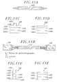
- FIGS. 11A and 11B the configuration before is illustrated resin and nitride removal, respectively after the first photolithography and after the second photolithography.
- the figures 11C and 11D represent vertical section views of the structure respectively at the second section 142 and first section 140, after the first engraving, and FIGS. 11E and 11F represent views similar in vertical sections respectively at the second section 142 and first section 140 after the second etching.
- the guides 14 are formed of substantially rectilinear segments between the lenses 10, 12.
- Each of the first sections 140 of a guide 14 is itself split into two segments 140A, 140B which surround a second section 142.
- the segments 140A and 140B and the section 142 are substantially aligned.
- the section 142 and the segment 140B are substantially aligned while the segment 140A is arranged in oblique, inclined to them.
- connection zones between the second section 142 and respectively each of the segments 140A, 140B are referenced 146, 147.
- this area is in the form of an isosceles triangle according to FIG. 4, the median plane of symmetry of the second sections 142 being perpendicular to the general direction of the guides and the areas of connection being symmetrical with respect to a plane orthogonal to this direction.
- the area of the second sections 142 is in the form of right triangle according to Figure 5, the connection area 146 being tilted on the general direction of the guides while the area of connection 147 is orthogonal to this general direction.
- the devices are long (about lmm), they are formed from a guide of very slight curvature. These guides as well reduce propagation losses compared to a PHASAR classic curved guide structure dependent on the temperature. To facilitate the understanding of straight lines rather than curves are shown in the accompanying figures. In reality, a curvature and a mode adapter are required to reduce loss of connection, between the structures of index n1 and n2, that is to say between the segments 140A, 140B and the second sections 142.
- This junction is shown schematically in Figure 4 and omitted on the FIGS. 5 and 6 to better show the structure of the segments 140A, 140B and second sections 142.
- the two sections 140, 142 can be formed by an end-to-end coupling between a guide 140 composed of semiconductor, for example InP and a polymer resin 142, for example of the type PMMA.
- the variation of the index with the temperature is positive for InP and negative for PMMA.
- K 1 (K always choose positive).
- each second section 142 is the still placed between two segments 140A, 140B of the first section 140.
- each second section 142 is itself split into two rectilinear segments orthogonal to each other 142A, 142B. These second segments 142A, 142B are coupled together by a 45 ° mirror. They are also coupled to a first segment 140A, 140B respective aligned. The mirrors 150 thus ensure the coupling between two similar segments 142A, 142B.
- Figure 9 corresponds to a guide configuration with classic turns in themselves.
- the mirrors 150 can for example be produced according to teaching of the document [6] FR-A-2725040 (patent application French n ° 94 11369).
- independence from polarization can also be set in the same way as for a phasar classic.
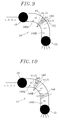
- each guide 14 comprises at least two sections 140, 142 ensuring control of the effects of temperature and at least one third section 144 in series on each guide of variable length from one guide to another in constant step ⁇ L3, ensuring compensation for the polarization, as shown schematically in Figure 10.
- each first section 140 is divided into three segments 140A, 140B, 140C which frame two by two respectively a second section 142 and a third section 144,
- ⁇ L can be negative.
- a example is given by figure 10: ⁇ L3 is of opposite sign to ⁇ L1 since it decreases towards the outside of the turn.
- the accuracy of the above system can be further improved by involving the variation of the length of the guide sections in temperature function.
- the values K1 and K2 are experimental data and contain both the variation of the index and the variation in length with temperature.
Landscapes
- Physics & Mathematics (AREA)
- Engineering & Computer Science (AREA)
- Microelectronics & Electronic Packaging (AREA)
- General Physics & Mathematics (AREA)
- Optics & Photonics (AREA)
- Optical Integrated Circuits (AREA)
Applications Claiming Priority (2)
| Application Number | Priority Date | Filing Date | Title |
|---|---|---|---|
| FR9615855 | 1996-12-23 | ||
| FR9615855A FR2757722B1 (fr) | 1996-12-23 | 1996-12-23 | Multiplexeur et/ou demultiplexeur optique independant de la temperature |
Publications (1)
| Publication Number | Publication Date |
|---|---|
| EP0851252A1 true EP0851252A1 (fr) | 1998-07-01 |
Family
ID=9499003
Family Applications (1)
| Application Number | Title | Priority Date | Filing Date |
|---|---|---|---|
| EP97403114A Withdrawn EP0851252A1 (fr) | 1996-12-23 | 1997-12-22 | Muliplexeur et/ou démultiplexeur optique indépendant de la température |
Country Status (4)
| Country | Link |
|---|---|
| US (1) | US6181848B1 (ja) |
| EP (1) | EP0851252A1 (ja) |
| JP (1) | JPH112731A (ja) |
| FR (1) | FR2757722B1 (ja) |
Cited By (2)
| Publication number | Priority date | Publication date | Assignee | Title |
|---|---|---|---|---|
| EP1219983A3 (en) * | 2000-12-22 | 2004-10-06 | Nippon Telegraph and Telephone Corporation | Polarization independent optical waveguide circuit |
| WO2006096602A2 (en) | 2005-03-04 | 2006-09-14 | Gemfire Corporation | Optical device with reduced temperature dependence |
Families Citing this family (21)
| Publication number | Priority date | Publication date | Assignee | Title |
|---|---|---|---|---|
| KR100327898B1 (ko) * | 1998-11-12 | 2002-08-21 | 한국전자통신연구원 | 직선형광도파로를구비한파장역다중화소자 |
| DE69938132T2 (de) | 1999-09-28 | 2009-03-05 | Corning Incorporated | Athermischer Wellenleitergitter-Multiplexer (AWG) mit Polymersegment, sowie entsprechendes Herstellungsverfahren |
| US6324204B1 (en) * | 1999-10-19 | 2001-11-27 | Sparkolor Corporation | Channel-switched tunable laser for DWDM communications |
| US6400860B1 (en) * | 2000-03-21 | 2002-06-04 | Lucent Technologies Inc. | Wavelength selective polarization beam splitter/combiner |
| US6466707B1 (en) | 2000-08-21 | 2002-10-15 | Corning Incorporated | Phasar athermalization using a slab waveguide |
| US6697552B2 (en) | 2001-02-23 | 2004-02-24 | Lightwave Microsystems Corporation | Dendritic taper for an integrated optical wavelength router |
| US6847477B2 (en) * | 2001-02-28 | 2005-01-25 | Kilolamdia Ip Limited | Optical system for converting light beam into plurality of beams having different wavelengths |
| US6853769B2 (en) * | 2001-03-16 | 2005-02-08 | Lightwave Microsystems Corporation | Arrayed waveguide grating with waveguides of unequal widths |
| JP2003005232A (ja) * | 2001-04-18 | 2003-01-08 | Ngk Insulators Ltd | 光デバイス |
| US6850670B2 (en) * | 2001-06-28 | 2005-02-01 | Lightwave Microsytstems Corporation | Method and apparatus for controlling waveguide birefringence by selection of a waveguide core width for a top clad |
| JP3643058B2 (ja) * | 2001-07-30 | 2005-04-27 | Tdk株式会社 | 導波路形回折格子 |
| EP1319967A1 (en) * | 2001-12-13 | 2003-06-18 | Alcatel | Athermal arrayed waveguide grating (AWG) having thermal compensation in the slab waveguide |
| IL147554A (en) * | 2002-01-10 | 2005-11-20 | Kiloambda Ip Ltd | Optical limiter |
| AU2003209561A1 (en) * | 2002-03-13 | 2003-09-22 | Kilolambda Ip Limited | Optical energy switching device and method |
| JP2007514117A (ja) * | 2003-10-09 | 2007-05-31 | キロランダ・テクノロジーズ・リミテッド | 光発熱式チップ |
| US7609917B2 (en) * | 2005-10-11 | 2009-10-27 | Lightwave Microsystems Corporation | Method and apparatus for controlling waveguide birefringence by selection of a waveguide core width for a top cladding |
| EP2307796A4 (en) * | 2008-06-24 | 2012-08-08 | Kilolambda Tech Ltd | WINDOW OF LIMITATION OF LIGHT |
| US20110142396A1 (en) * | 2009-10-07 | 2011-06-16 | Aidi Corporation | Athermal silicon photonics array waveguide grating (awg) employing different core geometries in the array waveguides |
| WO2011116333A1 (en) * | 2010-03-19 | 2011-09-22 | Gemfire Corporation | Arrayed waveguide grating compensated in temperature up to the second order with longitudinal slots therein |
| US8538212B2 (en) | 2011-06-03 | 2013-09-17 | Neophotonics Corporation | Thermally compensated arrayed waveguide grating assemblies |
| US9110232B2 (en) | 2011-06-03 | 2015-08-18 | Neophotonics Corporation | Thermally compensated arrayed waveguide grating assemblies |
Citations (3)
| Publication number | Priority date | Publication date | Assignee | Title |
|---|---|---|---|---|
| JPH05323246A (ja) * | 1992-05-18 | 1993-12-07 | Nippon Telegr & Teleph Corp <Ntt> | 光合分波器 |
| EP0662621A1 (de) * | 1994-01-11 | 1995-07-12 | Siemens Aktiengesellschaft | Optische Anordnung aus streifenförmigen optischen Wellenleitern |
| FR2732777A1 (fr) * | 1995-04-05 | 1996-10-11 | Bruno Adrien | Demultiplexeur insensible a la polarisation et procede de realisation |
Family Cites Families (7)
| Publication number | Priority date | Publication date | Assignee | Title |
|---|---|---|---|---|
| DE662621C (de) | 1934-12-12 | 1938-07-18 | Audrey Gretchen Coats Geb Wilm | Steilschrauberfluegel |
| US5341444A (en) * | 1993-03-19 | 1994-08-23 | At&T Bell Laboratories | Polarization compensated integrated optical filters and multiplexers |
| JPH0943440A (ja) * | 1995-07-28 | 1997-02-14 | Toshiba Corp | 集積化光合分波器 |
| US5623571A (en) * | 1995-08-29 | 1997-04-22 | Lucent Technologies Inc. | Polarization compensated waveguide grating router |
| EP0792469A1 (en) * | 1995-09-20 | 1997-09-03 | Koninklijke Philips Electronics N.V. | Integrated optical circuit comprising a polarization convertor |
| JP2858655B2 (ja) * | 1997-01-22 | 1999-02-17 | 日立電線株式会社 | 光波長合分波器 |
| US6049640A (en) * | 1997-09-04 | 2000-04-11 | Lucent Technologies Inc. | Wavelength-division-multiplexing cross-connect using angular dispersive elements and phase shifters |
-
1996
- 1996-12-23 FR FR9615855A patent/FR2757722B1/fr not_active Expired - Fee Related
-
1997
- 1997-12-22 EP EP97403114A patent/EP0851252A1/fr not_active Withdrawn
- 1997-12-22 US US08/995,965 patent/US6181848B1/en not_active Expired - Lifetime
- 1997-12-22 JP JP9353252A patent/JPH112731A/ja active Pending
Patent Citations (3)
| Publication number | Priority date | Publication date | Assignee | Title |
|---|---|---|---|---|
| JPH05323246A (ja) * | 1992-05-18 | 1993-12-07 | Nippon Telegr & Teleph Corp <Ntt> | 光合分波器 |
| EP0662621A1 (de) * | 1994-01-11 | 1995-07-12 | Siemens Aktiengesellschaft | Optische Anordnung aus streifenförmigen optischen Wellenleitern |
| FR2732777A1 (fr) * | 1995-04-05 | 1996-10-11 | Bruno Adrien | Demultiplexeur insensible a la polarisation et procede de realisation |
Non-Patent Citations (3)
| Title |
|---|
| BISSESSUR H ET AL: "EXTREMELY SMALL POLARIZATION INDEPENDENT PHASED-ARRAY DEMULTIPLEXERS ON INP", IEEE PHOTONICS TECHNOLOGY LETTERS, vol. 8, no. 4, 1 April 1996 (1996-04-01), pages 554 - 556, XP000587021 * |
| PATENT ABSTRACTS OF JAPAN vol. 018, no. 146 (P - 1707) 10 March 1994 (1994-03-10) * |
| RIGNY A ET AL: "TAPER-ASSISTED POLARISATION COMPENSATION IN EFFICIENTLY FIBRE-COUPLED INP DEMULTIPLEXER", ELECTRONICS LETTERS., vol. 32, no. 20, 26 September 1996 (1996-09-26), ENAGE GB, pages 1885/1886 - 1886, XP000637889 * |
Cited By (3)
| Publication number | Priority date | Publication date | Assignee | Title |
|---|---|---|---|---|
| EP1219983A3 (en) * | 2000-12-22 | 2004-10-06 | Nippon Telegraph and Telephone Corporation | Polarization independent optical waveguide circuit |
| WO2006096602A2 (en) | 2005-03-04 | 2006-09-14 | Gemfire Corporation | Optical device with reduced temperature dependence |
| EP1869515A4 (en) * | 2005-03-04 | 2012-02-01 | Gemfire Corp | OPTICAL DEVICE WITH REDUCED TEMPERATURE DEPENDENCE |
Also Published As
| Publication number | Publication date |
|---|---|
| FR2757722A1 (fr) | 1998-06-26 |
| US6181848B1 (en) | 2001-01-30 |
| FR2757722B1 (fr) | 1999-03-19 |
| JPH112731A (ja) | 1999-01-06 |
Similar Documents
| Publication | Publication Date | Title |
|---|---|---|
| EP0851252A1 (fr) | Muliplexeur et/ou démultiplexeur optique indépendant de la température | |
| EP2664949B1 (fr) | Coupleur optique séparateur de polarisation | |
| EP3491438B1 (fr) | Coupleur optique multi-spectral à faibles pertes en réception | |
| EP0911660A1 (fr) | Dispositif optique à réseau de phase et procédé de fabrication de celui-ci | |
| EP1191364A1 (en) | Waveguide optical interferometer | |
| EP0736785B1 (fr) | Démultiplexeur insensible à la polarisation et procédé de réalisation | |
| US9983359B2 (en) | Polarization-insensitive optical transceiver | |
| EP0703473B1 (fr) | Dispositif optoélectronique intégré pour la séparation de longueurs d'onde différentes et leur détection | |
| EP0783118A1 (fr) | Démultiplexeur en longueur d'onde | |
| US20230161101A1 (en) | Devices and methods exploiting waveguide supercells | |
| EP0916977A1 (fr) | Demultiplexeur à réponse spectrale carree | |
| EP0831346A1 (fr) | Composant multiplexeur à spectographe à réseau de guide d'onde | |
| WO2002077687A2 (fr) | Spectrometre optique integre a haute resolution spectrale et procede de fabrication | |
| CA2311157A1 (fr) | Multiplexeur/demultiplexeur optique a trois guides d'onde | |
| CA2160217C (fr) | Coupleur optique selectif en longueur d'onde | |
| EP0465425A1 (fr) | Dispositif optique intégré séparateur de polarisation, utilisation de ce dispositif et système optique intégré interférométrique obtenu | |
| Melati et al. | Athermal echelle grating and tunable echelle grating demultiplexers using a Mach-Zehnder interferometer launch structure | |
| Wang et al. | Low-Crosstalk 1× 40 100 GHz Spacing Cascaded Planar Echelle Gratings for Mux/Demux on 3-μm Silicon Platform | |
| Vyrsokinos et al. | MOICANA: monolithic cointegration of QD-based InP on SiN as a versatile platform for the demonstration of high-performance and low-cost PIC transmitters | |
| EP3599501B1 (fr) | Modulateur-commutateur athermique à deux anneaux superposés | |
| FR2794858A1 (fr) | Dispositif analyseur de spectre optique a reseau de diffraction en optique integree | |
| FR3025659A1 (fr) | Source laser multi-longueurs d'onde auto-alignee et emetteur-recepteur integrant une telle source | |
| EP0921423A1 (fr) | Composant optique à spectrographe à réseau de guides, à géométrie de réseau améliorée | |
| EP0921422A1 (fr) | Composant optique de type à spectrographe à réseau de guides, à canaux de sortie centrés | |
| Zhang et al. | Integrating angled multimode interferometer with Bragg grating filters for coarse wavelength division (de) multiplexing with optimized shape factor |
Legal Events
| Date | Code | Title | Description |
|---|---|---|---|
| PUAI | Public reference made under article 153(3) epc to a published international application that has entered the european phase |
Free format text: ORIGINAL CODE: 0009012 |
|
| AK | Designated contracting states |
Kind code of ref document: A1 Designated state(s): DE GB |
|
| AX | Request for extension of the european patent |
Free format text: AL;LT;LV;MK;RO;SI |
|
| 17P | Request for examination filed |
Effective date: 19981221 |
|
| AKX | Designation fees paid |
Free format text: DE GB |
|
| RBV | Designated contracting states (corrected) |
Designated state(s): DE GB |
|
| RAP1 | Party data changed (applicant data changed or rights of an application transferred) |
Owner name: ALCATEL |
|
| RAP1 | Party data changed (applicant data changed or rights of an application transferred) |
Owner name: AVANEX CORPORATION |
|
| 17Q | First examination report despatched |
Effective date: 20041116 |
|
| STAA | Information on the status of an ep patent application or granted ep patent |
Free format text: STATUS: THE APPLICATION IS DEEMED TO BE WITHDRAWN |
|
| 18D | Application deemed to be withdrawn |
Effective date: 20050330 |