EP0851676A2 - Programmable clock generator for an imaging device - Google Patents
Programmable clock generator for an imaging device Download PDFInfo
- Publication number
- EP0851676A2 EP0851676A2 EP97204020A EP97204020A EP0851676A2 EP 0851676 A2 EP0851676 A2 EP 0851676A2 EP 97204020 A EP97204020 A EP 97204020A EP 97204020 A EP97204020 A EP 97204020A EP 0851676 A2 EP0851676 A2 EP 0851676A2
- Authority
- EP
- European Patent Office
- Prior art keywords
- clock
- imaging device
- shift register
- signal
- programmable
- Prior art date
- Legal status (The legal status is an assumption and is not a legal conclusion. Google has not performed a legal analysis and makes no representation as to the accuracy of the status listed.)
- Withdrawn
Links
Images

Classifications
-
- G—PHYSICS
- G06—COMPUTING OR CALCULATING; COUNTING
- G06F—ELECTRIC DIGITAL DATA PROCESSING
- G06F1/00—Details not covered by groups G06F3/00 - G06F13/00 and G06F21/00
- G06F1/02—Digital function generators
- G06F1/025—Digital function generators for functions having two-valued amplitude, e.g. Walsh functions
Definitions
- the invention relates generally to the field of digital integrated circuits, and in particular to the generation of periodic signals useful in digital integrated circuits. More specifically, the invention relates to the generation of clock signals for an imaging device.
- CCD imager In digital integrated circuits which must produce a wide variety of signal patterns, it is often necessary to design special counters and/or state machines to produce the desired results.
- An example of this application is in the field of digital imaging, where a charge coupled device (CCD) imager is employed in much the same manner as traditional silver-halide film.
- a CCD imager is a digital device which usually requires a substantial number of input signals with specific and unique characteristics. These signals are often referred to as "clocks", since they are usually periodic in nature.
- clocks since they are usually periodic in nature.
- an imaging device for generating an image signal comprises an image sensing device for producing an image signal subject to one or more clock signals and means for generating said one or more clock signals, wherein the clock signal generating means is responsive to a programmable input signal for adjusting a duty cycle of at least one of the clock signals.
- the frequency of an input clock signal that is required to produce the different output clock signals can be reduced by half. Reducing clock frequency results in several advantages, such as reducing EMI and potentially allowing the use of field programmable gate array technology to quickly prototype the hardware system.
- the pulse widths and the positioning of the output pulses are programmable, thus obviating the need to physically change hardware if empirical techniques are required to determine proper pulse timing within an actual electronic system. Pulse width and positioning are also as accurate and precise as the quartz crystal oscillator required to produce the digital system clocks. This may provide an advantage over many analog delay techniques, which are subject to the wider tolerances of discrete passive components.
- the invention can be implemented as part of an ASIC for as little as 200 to 300 gates per output signal, thus adding little, if any, cost to the overall system.
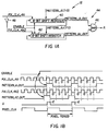
- FIG. 1A is a diagram of a programmable clock generator according to the invention.
- FIG. 1B is a timing diagram of the signals applied to, and produced by, the clock generator shown in Figure 1A.
- FIG. 2A is a diagram of a second implementation of a programmable clock generator according to the invention.
- FIG. 2B is a timing diagram for the clock generator shown in Figure 2A.
- FIG. 3 is a diagram of a third implementation of a programmable clock generator according to the invention.
- FIG. 4 is a diagram of a fourth implementation of a programmable clock generator according to the invention.
- FIG. 5 is a block diagram of an imaging device employing a clock generator of the type shown in Figures 1A, 2A, 3 or 4.
- an imaging device 10 is shown in a block diagram incorporating a clock generator 12 according to the invention.
- the clock generator 12 is used to drive, i.e., "clock", an image sensor 14, such as a charge-coupled device (CCD) sensor, which receives an image of an object 16 through an optical section 18.
- a master clock generator section 19 provides a relatively low frequency pixel clock (PIXEL_CLK) and a higher frequency 4X pixel clock (PIX_CLK_4X) to the clock generator 12.
- PIXEL_CLK relatively low frequency pixel clock
- PIX_CLK_4X 4X pixel clock
- the image sensor 14 requires a number of input clock signals 20 with characteristics specific to the type of sensor employed.
- the clock signals 20 are used, among other things, to output an image signal to an analog processing section 22, which adjusts the signal, e.g., for black level and gain.
- the image signal is then digitized in an analog-to-digital (A/D) converter 24 and output to a digital signal processing section 26, which may, e.g., apply a known compression algorithm, correct for sensor defects, interpolate for full color (if the sensor 14 is a color sensor), and the like.
- the digitally processed signal is then available for conventional utilization, e.g., transmission, storage, hard copy output, and so on.
- the various elements of the imaging device 10 are controlled by a microprocessor 28.
- the microprocessor 28 provides a clocking PATTERN signal, via a data channel, and an ENABLE command to the clock generator 12 in order to begin a clocking sequence.
- the PATTERN signal modifies the duty cycles of the clock signals 20.
- the clock generator 12 comprises two serial shift registers 40 and 42 and an output decoding logic section 44, in this case an AND gate 46.
- the first shift register 40 is clocked by the PIX_CLK_4X signal
- the second shift register 42 is clocked by a PIX_CLK_4XZ signal, which is an inverted form of the PIX_CLK_4X signal as output by an inverter 48.
- the registers 40 and 42 are clocked out of phase with the output of one shift register or the other being updated every half period of the PIX_CLK_4X signal.
- Both shift registers 40 and 42 are parallel-in, serial-out registers, with initialization data input in parallel to set up the registers.
- respective parallel-in signals PATTERN_A and PATTERN_AZ are loaded into the respective shift registers 40 and 42 when the ENABLE signal is asserted by the microprocessor 28.
- the outputs of the shift registers 40 and 42 are connected to their respective inputs to form recirculating shift registers in which the pattern loaded into each shift register repeats in a periodic fashion.
- the shift register output signals PATTERN_A_OUT and PATTERN_AZ_OUT are then decoded in the logic section 44 to produce the final output signal.
- the pattern data loaded into each shift register 40 and 42 is chosen such that the only output decoding logic required is the AND function provided by the gate 46.
- the clock generator 12 uses AND logic gates and 8-bit shift registers to produce a simple programmable timing generator. As shown in the timing diagram of Figure 1B, two eight bit patterns (each 10001000) are parallel loaded into the shift registers 40 and 42. However, the scope of the invention does not preclude the use of other initialization patterns and other logic decoding techniques.
- the circuit shown in Figure 1A is duplicated in the clock generator 12 for as many clock signals as are required to operate the image sensor 14. The microprocessor 28 would accordingly provide corresponding clocking PATTERN signals and control signals for these additional clock generator circuits.
- both PATTERN_A and PATTERN_AZ are loaded into their respective shift registers 40 and 42 before the shift registers are enabled.
- the ENABLE signal is asserted by the microprocessor 28
- the patterns loaded into each shift register are clocked out in a serial fashion. Since the shift register outputs are connected to their inputs, the pattern repeats in a periodic fashion producing the waveforms labeled PATTERN_A_OUT and PATTERN_AZ_OUT.
- Output signal A from the AND gate 46 is the logical combination of PATTERN_A_OUT and PATTERN_AZ_OUT.
- the pattern signals PATTERN_A and PATTERN_AZ overlap. This prevents glitching (i.e., generation of signal artifacts) in the output pulse signal A.
- the position of output pulse A and the width of output pulse A can be varied in increments of one-half the PIX_CLK_4X period by simply changing the initialization patterns which are loaded into the serial shift registers.
- the PIXEL_CLK signal which is one of the clock signals 20 shown in Figure 5, is shown to demonstrate how this invention could be used to generate the CCD timing clocks in a digital imaging system, specifically in this case, a CCD RESET pulse.
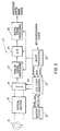
- Figure 2A shows a second embodiment of the clock generator 12 employing a single eight bit shift register 50, with its output recirculated back to its input.
- the same output as in Figure 1B is obtained by running the CLK signal at 8 times the pixel clock (PIX_CLK_8X), in order to produce the same pulse widths, and using an eight bit pattern such as 00010000 or any variation thereof with, e.g., seven zeros and one bit.
- the timing diagram for the single shift register 50 is shown in Figure 2B, particularly showing the output of a plurality of clock signals OUT1...OUTN from respective output taps. (The shift register would of course allow the output of as many clock signals as there are output taps, were that to be necessary.)
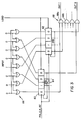
- FIG 3 shows a third embodiment of the clock generator 12, which is basically a variation of the circuit shown in Figure 1A.
- Two four bit shift registers 60 and 62 are clocked out of phase by the clock signal PIX_CLK_4X, which is four times the PIXEL_CLK signal shown in Figure 1B.
- the first shift register 60 is directly clocked by the PIX_CLK_4X signal, and the second shift register 62 by the same signal after being inverted in an inverter 64.
- the same pattern signal is input to both registers 60 and 62 through a set 66 of OR gates.
- This OR configuration allows the programmer to enter the desired final pattern (e.g., 10000000, corresponding to the duty cycle of the A signal in Figure 1B), rather than entering a pre-encoded pattern (e.g., the 10001000 pattern entered in Figure 1B), making it easier and more intuitive to program.
- the outputs OUT1...OUTN are taken through a set 68 of AND gates connected to corresponding sections of each shift registers, i.e., AND gate 68a is connected to the first sections of shift registers 60 and 62, gate 68b to the second sections, and so on.
- This diagram thus provides four clock signal outputs according to the timing relationship shown in Figure 1B.
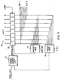
- Figure 4 shows a fourth embodiment of the clock generator 12, which has the advantage of a lower input clock frequency, more accurate edge positioning, and output pulse widths and pulse positionings that are other than powers of two (i.e., 1/3, 1/5, 1/6, 1/7) of the input pixel clock.
- a shift register 70 is clocked by the output of a phase locked loop 72, which receives the PIXEL_CLK signal and outputs a multiple nX of the pixel clock (PIX_CLK_nX) to a clock input of the shift register 70.
- the tap corresponding to the rising edge (pulse) of an input pattern 74 is selected by a phase multiplexer 76 so that the output thereof can be frequency locked to the PIXEL_CLK signal input to the phase locked loop 72.
- the modulus of the shift register 70 is determined by a modulo multiplexer 78, which responds to a MOD_SEL input and chooses a desired end tap of the shift register 70. Different end taps cause different lengths of the shift register 70 to be recirculated, thereby changing the repetition rate of the output pulses and therefore the pulse positioning. Therefore, a modulus can be chosen (e.g., tap 6) which generates an output pulse width (e.g., 1/6) that is not based on a power of two proportion of the PIXEL_CLK signal period.
- An output clock signal OUT1...OUTN can be taken from any of the shift register taps, and the repetition rate of an edge at the chosen output tap will depend on the tap selected by the modulo multiplexer 78.
- the invention provides a number of key advantages over the prior art, including:
- An imaging device for generating an image signal, said imaging device comprising: an image sensing device for producing an image signal subject to one or more clock signals; a clock generator for generating said one or more clock signals, said clock generator responsive to a programmable input signal for adjusting a phase and/or duty cycle of at least one of said clock signals; and a microprocessor for providing the programmable input signal to the clock generator.
- An imaging device in which said clock generation means uses a shift register uses a shift register.
- a clock generator for generating one or more clock signals, said clock generator comprising: a pair of shift registers each connected to recirculate their output back to their input, each shift register including a plurality of sections and each shift register responsive to a parallel input of a programmable bit pattern; means for clocking the shift registers out of phase; and a logic section having inputs connected to corresponding sections of each shift register for providing the one or more clock signals.
- a clock generator in which the programmable bit pattern is input to said pair of shift registers through a set of OR gates that are connected to the sections of the shift registers.
- Apparatus for generating an electronic version of an image comprising: an image sensing device for converting light into an image-bearing signal in response to clocks; and means for generating clocks for said image sensing device wherein said clock generating means is programmable via a processor interface of clock phase and/or duty cycle.
- An apparatus in which said clock generation means includes a shift register.
Landscapes
- Engineering & Computer Science (AREA)
- Theoretical Computer Science (AREA)
- Physics & Mathematics (AREA)
- General Engineering & Computer Science (AREA)
- General Physics & Mathematics (AREA)
- Transforming Light Signals Into Electric Signals (AREA)
Abstract
Description
- 10
- imaging device
- 12
- clock generator
- 14
- image sensor
- 16
- object
- 18
- optical section
- 20
- input clock signals
- 22
- analog signal processing section
- 24
- A/D converter
- 26
- digital signal processing section
- 28
- microprocessor
- 40
- first serial shift register
- 42
- second serial shift register
- 44
- logic section
- 46
- AND gate
- 48
- inverter
- 50
- light bit shift register
- 60
- first four bit shift register
- 62
- second four bit shift register
- 64
- inverter
- 66
- set of OR gates
- 68
- set of AND gates
- 70
- shift register
- 72
- phase locked loop
- 74
- input pattern
- 76
- phase multiplexer
- 78
- modulo multiplexer
Claims (9)
- An imaging device for generating an image signal, said imaging device comprising:an image sensing device for producing an image signal subject to one or more clock signals; andmeans for generating said one or more clock signals, said clock signal generating means responsive to a programmable input signal for adjusting a phase and/or duty cycle of at least one of said clock signals.
- An imaging device as claimed in claim 1 in which said clock generation means includes a shift register.
- An imaging device as claimed in claim 2 in which said programmable input signal is parallel-loaded into the shift register, and the shift register is connected into a recirculating configuration.
- An imaging device as claimed in claim 1 in which said clock generator means includes multiple shift registers clocked out of phase.
- An imaging device as claimed in claim 4 in which said programmable input signal is parallel-loaded into each shift register, and each shift register is connected into a recirculating configuration.
- An imaging device as claimed in claim 2 where said shift register has a programmable modulo.
- An imaging device as claimed in claim 6 wherein the programmable modulo is provided by a multiplexer that selectively connects different lengths of the register into a recirculating configuration.
- An imaging device as claimed in claim 1 in which the clock generation means includes a shift register coupled into a phase locked loop having a pair of inputs, said shift register having a clock input and individual sections each having a tap output, said clock generation means further having means for coupling a selected tap output to one of the inputs of the phase locked loop, said phase locked loop receiving a system clock on its other input and having an output connected to the clock input of the shift register.
- An imaging device as claimed in claim 8 wherein said means for coupling a selected tap output comprises a multiplexer.
Applications Claiming Priority (2)
| Application Number | Priority Date | Filing Date | Title |
|---|---|---|---|
| US08/777,430 US5982428A (en) | 1996-12-30 | 1996-12-30 | Programmable clock generator for an imaging device |
| US777430 | 1996-12-30 |
Publications (2)
| Publication Number | Publication Date |
|---|---|
| EP0851676A2 true EP0851676A2 (en) | 1998-07-01 |
| EP0851676A3 EP0851676A3 (en) | 1999-07-28 |
Family
ID=25110240
Family Applications (1)
| Application Number | Title | Priority Date | Filing Date |
|---|---|---|---|
| EP97204020A Withdrawn EP0851676A3 (en) | 1996-12-30 | 1997-12-19 | Programmable clock generator for an imaging device |
Country Status (3)
| Country | Link |
|---|---|
| US (1) | US5982428A (en) |
| EP (1) | EP0851676A3 (en) |
| JP (1) | JPH10210368A (en) |
Cited By (1)
| Publication number | Priority date | Publication date | Assignee | Title |
|---|---|---|---|---|
| US7131022B2 (en) | 2002-04-10 | 2006-10-31 | Axis Ab | Timing generator system for outputting clock signals to components of an imaging system according to decoded timing control instructions |
Families Citing this family (10)
| Publication number | Priority date | Publication date | Assignee | Title |
|---|---|---|---|---|
| US6580456B1 (en) * | 1997-11-16 | 2003-06-17 | Pictos Technologies, Inc. | Programmable timing generator |
| JP4088855B2 (en) * | 1999-03-26 | 2008-05-21 | 富士フイルム株式会社 | Timing pulse generator |
| US6784929B1 (en) * | 1999-08-20 | 2004-08-31 | Infineon Technologies North America Corp. | Universal two dimensional (frame and line) timing generator |
| US7586526B2 (en) * | 2001-03-29 | 2009-09-08 | Canon Kabushiki Kaisha | Image sensing apparatus with at least two transfer speeds and its control method |
| US20020191094A1 (en) * | 2001-05-30 | 2002-12-19 | Eastman Kodak Company | CCD clock alignment circuit using a frequency locked clock multiplier |
| TW548952B (en) * | 2001-12-31 | 2003-08-21 | Winbond Electronics Corp | Control system and method of CCD device in scanner |
| US7012646B2 (en) * | 2002-04-04 | 2006-03-14 | Eastman Kodak Company | Reset driver circuit disposed on the same substrate as the image sensor |
| US20040090248A1 (en) * | 2002-09-20 | 2004-05-13 | Eastman Kodak Company | Programmable timing generator with offset and width control using delay lock loop |
| WO2006023726A1 (en) | 2004-08-19 | 2006-03-02 | Intrinsix Corporation | Hybrid heterodyne transmitters and receivers |
| US8654555B2 (en) | 2012-06-04 | 2014-02-18 | Raytheon Company | ROIC control signal generator |
Family Cites Families (10)
| Publication number | Priority date | Publication date | Assignee | Title |
|---|---|---|---|---|
| JPS60179814A (en) * | 1984-02-27 | 1985-09-13 | Fujitsu Ltd | Circuit for forming clock having period of n times |
| JPS61137414A (en) * | 1984-12-10 | 1986-06-25 | Matsushita Electric Ind Co Ltd | Simple variable duty pulse generation circuit |
| JPH01236813A (en) * | 1988-03-17 | 1989-09-21 | Nec Corp | N-phase clock generating circuit |
| US4922137A (en) * | 1988-05-17 | 1990-05-01 | Eastman Kodak Company | Programmable sequence generator |
| US5039950A (en) * | 1989-07-20 | 1991-08-13 | Eastman Kodak Company | Multiple clock synthesizer |
| EP0467683A3 (en) * | 1990-07-19 | 1992-09-02 | Canon Kabushiki Kaisha | Image processing apparatus |
| US5321315A (en) * | 1992-03-09 | 1994-06-14 | Eastman Kodak Company | Tracking control pulse generation for variable frame rate CCD sensors for electronic imaging applications |
| JP2744577B2 (en) * | 1993-06-30 | 1998-04-28 | 池上通信機株式会社 | Image phase adjustment circuit for solid-state imaging device |
| JP3361188B2 (en) * | 1994-06-16 | 2003-01-07 | 富士写真フイルム株式会社 | Electronic still camera and operation control method thereof |
| JP3607325B2 (en) * | 1994-09-22 | 2005-01-05 | 株式会社アドバンテスト | Comparison circuit for semiconductor test equipment |
-
1996
- 1996-12-30 US US08/777,430 patent/US5982428A/en not_active Expired - Lifetime
-
1997
- 1997-12-19 EP EP97204020A patent/EP0851676A3/en not_active Withdrawn
- 1997-12-25 JP JP9357991A patent/JPH10210368A/en active Pending
Cited By (1)
| Publication number | Priority date | Publication date | Assignee | Title |
|---|---|---|---|---|
| US7131022B2 (en) | 2002-04-10 | 2006-10-31 | Axis Ab | Timing generator system for outputting clock signals to components of an imaging system according to decoded timing control instructions |
Also Published As
| Publication number | Publication date |
|---|---|
| JPH10210368A (en) | 1998-08-07 |
| EP0851676A3 (en) | 1999-07-28 |
| US5982428A (en) | 1999-11-09 |
Similar Documents
| Publication | Publication Date | Title |
|---|---|---|
| US6292040B1 (en) | Internal clock signal generating circuit having function of generating internal clock signals which are multiplication of an external clock signal | |
| US5119045A (en) | Pulse width modulation circuit | |
| JP2930978B2 (en) | Device for synchronizing clock signals | |
| US5982428A (en) | Programmable clock generator for an imaging device | |
| JP2002025259A (en) | Register control delay fixed loop utilizing ring delay and counter | |
| US6040725A (en) | Dynamically configurable variable frequency and duty cycle clock and signal generation | |
| EP0717496B1 (en) | High speed parallel/serial interface | |
| US5511181A (en) | Polycyclic timing system and apparatus for pipelined computer operation | |
| US5634116A (en) | Non-integer multiple clock translator | |
| US5122761A (en) | Digital pll including controllable delay circuit | |
| JPH04268811A (en) | Timing generator | |
| US5847588A (en) | Programmable multiple CCD clock synthesizer | |
| US4922137A (en) | Programmable sequence generator | |
| US6633995B1 (en) | System for generating N pipeline control signals by delaying at least one control signal corresponding to a subsequent data path circuit | |
| KR950001263B1 (en) | High speed signal multiplexing device | |
| KR100321732B1 (en) | Delay Locked Loop using Digital Ring Synchronous Mirror Delay | |
| US7518648B2 (en) | Horizontal register transfer pulse generation circuit and imaging apparatus | |
| EP1618660B1 (en) | Enabling method to prevent glitches in waveform | |
| KR19980050372A (en) | Clock generator for data transmission synchronization | |
| JPS62202624A (en) | High speed data reception circuit system | |
| JP3337873B2 (en) | Anti-collision device | |
| JP2004345280A (en) | Digital PWM signal generation circuit | |
| JP3302023B2 (en) | Signal synchronization device and image recording device | |
| US5565797A (en) | Clock signal generating device | |
| JPH05101204A (en) | Data processing system |
Legal Events
| Date | Code | Title | Description |
|---|---|---|---|
| PUAI | Public reference made under article 153(3) epc to a published international application that has entered the european phase |
Free format text: ORIGINAL CODE: 0009012 |
|
| AK | Designated contracting states |
Kind code of ref document: A2 Designated state(s): AT BE CH DE DK ES FI FR GB GR IE IT LI LU MC NL PT SE |
|
| AX | Request for extension of the european patent |
Free format text: AL;LT;LV;MK;RO;SI |
|
| PUAL | Search report despatched |
Free format text: ORIGINAL CODE: 0009013 |
|
| AK | Designated contracting states |
Kind code of ref document: A3 Designated state(s): AT BE CH DE DK ES FI FR GB GR IE IT LI LU MC NL PT SE |
|
| AX | Request for extension of the european patent |
Free format text: AL;LT;LV;MK;RO;SI |
|
| AKX | Designation fees paid | ||
| REG | Reference to a national code |
Ref country code: DE Ref legal event code: 8566 |
|
| STAA | Information on the status of an ep patent application or granted ep patent |
Free format text: STATUS: THE APPLICATION IS DEEMED TO BE WITHDRAWN |
|
| 18D | Application deemed to be withdrawn |
Effective date: 20000129 |