EP0854350B1 - Réseau de sondes pour une sonde microscope à balayage - Google Patents
Réseau de sondes pour une sonde microscope à balayage Download PDFInfo
- Publication number
- EP0854350B1 EP0854350B1 EP97122587A EP97122587A EP0854350B1 EP 0854350 B1 EP0854350 B1 EP 0854350B1 EP 97122587 A EP97122587 A EP 97122587A EP 97122587 A EP97122587 A EP 97122587A EP 0854350 B1 EP0854350 B1 EP 0854350B1
- Authority
- EP
- European Patent Office
- Prior art keywords
- probe
- bars
- individual probes
- probe array
- grid
- Prior art date
- Legal status (The legal status is an assumption and is not a legal conclusion. Google has not performed a legal analysis and makes no representation as to the accuracy of the status listed.)
- Expired - Lifetime
Links
- 239000000523 sample Substances 0.000 title claims description 183
- 125000006850 spacer group Chemical group 0.000 claims description 8
- 238000000576 coating method Methods 0.000 description 14
- 229910052581 Si3N4 Inorganic materials 0.000 description 6
- 239000003990 capacitor Substances 0.000 description 6
- 239000011248 coating agent Substances 0.000 description 6
- 238000000034 method Methods 0.000 description 6
- 239000013598 vector Substances 0.000 description 6
- 239000004020 conductor Substances 0.000 description 5
- 230000003287 optical effect Effects 0.000 description 5
- HQVNEWCFYHHQES-UHFFFAOYSA-N silicon nitride Chemical compound N12[Si]34N5[Si]62N3[Si]51N64 HQVNEWCFYHHQES-UHFFFAOYSA-N 0.000 description 5
- 238000000386 microscopy Methods 0.000 description 4
- 238000003491 array Methods 0.000 description 3
- 238000005452 bending Methods 0.000 description 3
- 230000003993 interaction Effects 0.000 description 3
- 239000000758 substrate Substances 0.000 description 3
- XUIMIQQOPSSXEZ-UHFFFAOYSA-N Silicon Chemical compound [Si] XUIMIQQOPSSXEZ-UHFFFAOYSA-N 0.000 description 2
- XLOMVQKBTHCTTD-UHFFFAOYSA-N Zinc monoxide Chemical compound [Zn]=O XLOMVQKBTHCTTD-UHFFFAOYSA-N 0.000 description 2
- 238000000347 anisotropic wet etching Methods 0.000 description 2
- 239000013078 crystal Substances 0.000 description 2
- 239000013307 optical fiber Substances 0.000 description 2
- BASFCYQUMIYNBI-UHFFFAOYSA-N platinum Chemical compound [Pt] BASFCYQUMIYNBI-UHFFFAOYSA-N 0.000 description 2
- 238000002360 preparation method Methods 0.000 description 2
- 229910052710 silicon Inorganic materials 0.000 description 2
- 239000010703 silicon Substances 0.000 description 2
- NHWNVPNZGGXQQV-UHFFFAOYSA-J [Si+4].[O-]N=O.[O-]N=O.[O-]N=O.[O-]N=O Chemical compound [Si+4].[O-]N=O.[O-]N=O.[O-]N=O.[O-]N=O NHWNVPNZGGXQQV-UHFFFAOYSA-J 0.000 description 1
- 229910052782 aluminium Inorganic materials 0.000 description 1
- XAGFODPZIPBFFR-UHFFFAOYSA-N aluminium Chemical compound [Al] XAGFODPZIPBFFR-UHFFFAOYSA-N 0.000 description 1
- 230000008878 coupling Effects 0.000 description 1
- 238000010168 coupling process Methods 0.000 description 1
- 238000005859 coupling reaction Methods 0.000 description 1
- 238000005520 cutting process Methods 0.000 description 1
- 230000001419 dependent effect Effects 0.000 description 1
- 230000023077 detection of light stimulus Effects 0.000 description 1
- 238000010586 diagram Methods 0.000 description 1
- 238000006073 displacement reaction Methods 0.000 description 1
- 230000000694 effects Effects 0.000 description 1
- 238000005516 engineering process Methods 0.000 description 1
- PCHJSUWPFVWCPO-UHFFFAOYSA-N gold Chemical compound [Au] PCHJSUWPFVWCPO-UHFFFAOYSA-N 0.000 description 1
- 239000010931 gold Substances 0.000 description 1
- 229910052737 gold Inorganic materials 0.000 description 1
- 238000003384 imaging method Methods 0.000 description 1
- 150000002500 ions Chemical class 0.000 description 1
- 238000004519 manufacturing process Methods 0.000 description 1
- 239000000463 material Substances 0.000 description 1
- 238000005259 measurement Methods 0.000 description 1
- 229910052751 metal Inorganic materials 0.000 description 1
- 239000002184 metal Substances 0.000 description 1
- 238000004377 microelectronic Methods 0.000 description 1
- 238000001527 near-field phase shift lithography Methods 0.000 description 1
- 238000000399 optical microscopy Methods 0.000 description 1
- 229910052697 platinum Inorganic materials 0.000 description 1
- 230000001105 regulatory effect Effects 0.000 description 1
- 230000035945 sensitivity Effects 0.000 description 1
- 238000007740 vapor deposition Methods 0.000 description 1
- 239000011787 zinc oxide Substances 0.000 description 1
Images


Classifications
-
- G—PHYSICS
- G01—MEASURING; TESTING
- G01Q—SCANNING-PROBE TECHNIQUES OR APPARATUS; APPLICATIONS OF SCANNING-PROBE TECHNIQUES, e.g. SCANNING PROBE MICROSCOPY [SPM]
- G01Q60/00—Particular types of SPM [Scanning Probe Microscopy] or microscopes; Essential components thereof
- G01Q60/18—SNOM [Scanning Near-Field Optical Microscopy] or apparatus therefor, e.g. SNOM probes
- G01Q60/22—Probes, their manufacture, or their related instrumentation, e.g. holders
-
- B—PERFORMING OPERATIONS; TRANSPORTING
- B82—NANOTECHNOLOGY
- B82Y—SPECIFIC USES OR APPLICATIONS OF NANOSTRUCTURES; MEASUREMENT OR ANALYSIS OF NANOSTRUCTURES; MANUFACTURE OR TREATMENT OF NANOSTRUCTURES
- B82Y15/00—Nanotechnology for interacting, sensing or actuating, e.g. quantum dots as markers in protein assays or molecular motors
-
- B—PERFORMING OPERATIONS; TRANSPORTING
- B82—NANOTECHNOLOGY
- B82Y—SPECIFIC USES OR APPLICATIONS OF NANOSTRUCTURES; MEASUREMENT OR ANALYSIS OF NANOSTRUCTURES; MANUFACTURE OR TREATMENT OF NANOSTRUCTURES
- B82Y20/00—Nanooptics, e.g. quantum optics or photonic crystals
-
- B—PERFORMING OPERATIONS; TRANSPORTING
- B82—NANOTECHNOLOGY
- B82Y—SPECIFIC USES OR APPLICATIONS OF NANOSTRUCTURES; MEASUREMENT OR ANALYSIS OF NANOSTRUCTURES; MANUFACTURE OR TREATMENT OF NANOSTRUCTURES
- B82Y35/00—Methods or apparatus for measurement or analysis of nanostructures
-
- G—PHYSICS
- G01—MEASURING; TESTING
- G01Q—SCANNING-PROBE TECHNIQUES OR APPARATUS; APPLICATIONS OF SCANNING-PROBE TECHNIQUES, e.g. SCANNING PROBE MICROSCOPY [SPM]
- G01Q20/00—Monitoring the movement or position of the probe
- G01Q20/02—Monitoring the movement or position of the probe by optical means
-
- G—PHYSICS
- G01—MEASURING; TESTING
- G01Q—SCANNING-PROBE TECHNIQUES OR APPARATUS; APPLICATIONS OF SCANNING-PROBE TECHNIQUES, e.g. SCANNING PROBE MICROSCOPY [SPM]
- G01Q70/00—General aspects of SPM probes, their manufacture or their related instrumentation, insofar as they are not specially adapted to a single SPM technique covered by group G01Q60/00
- G01Q70/02—Probe holders
-
- G—PHYSICS
- G01—MEASURING; TESTING
- G01Q—SCANNING-PROBE TECHNIQUES OR APPARATUS; APPLICATIONS OF SCANNING-PROBE TECHNIQUES, e.g. SCANNING PROBE MICROSCOPY [SPM]
- G01Q70/00—General aspects of SPM probes, their manufacture or their related instrumentation, insofar as they are not specially adapted to a single SPM technique covered by group G01Q60/00
- G01Q70/06—Probe tip arrays
-
- Y—GENERAL TAGGING OF NEW TECHNOLOGICAL DEVELOPMENTS; GENERAL TAGGING OF CROSS-SECTIONAL TECHNOLOGIES SPANNING OVER SEVERAL SECTIONS OF THE IPC; TECHNICAL SUBJECTS COVERED BY FORMER USPC CROSS-REFERENCE ART COLLECTIONS [XRACs] AND DIGESTS
- Y10—TECHNICAL SUBJECTS COVERED BY FORMER USPC
- Y10S—TECHNICAL SUBJECTS COVERED BY FORMER USPC CROSS-REFERENCE ART COLLECTIONS [XRACs] AND DIGESTS
- Y10S977/00—Nanotechnology
- Y10S977/84—Manufacture, treatment, or detection of nanostructure
- Y10S977/849—Manufacture, treatment, or detection of nanostructure with scanning probe
- Y10S977/86—Scanning probe structure
- Y10S977/874—Probe tip array
Definitions
- US Pat. No. 5,015,850 describes a probe array for scanning probe microscopes, especially for tunnel and power microscopes, known.
- the individual probes each consist of a thin one Beam that can be deflected perpendicular to its longitudinal direction, and one located at the free end of the beam Probe tip.
- These individual probes are as two-dimensional Grid arranged, the longitudinal axes of the beams parallel to a lattice direction of the two-dimensional lattice are aligned.
- the distances between the probe tips are therefore much larger in one direction than the length the bar. With this arrangement are therefore at least in no probe distances can be achieved in one direction of the array are smaller than the bar lengths.
- a probe array according to the The preamble of claim 1 is known.
- the individual probes of the Probe arrays are bimorphic directly from a substrate Piezo material shaped by U-shaped cutouts. This Arrangement of the individual probes enables probe distances that are smaller than the length of the bars of the individual probes.
- the Rigidity of the substrate perpendicular to the beam direction However, individual probes correspond to the rigidity of the bars and is accordingly low.
- From US 5 517 280 is a one-dimensional linear Probe array known for near field photolithography. at the individual probe tips are in this arrangement deflectable bars arranged. The individual bars are arranged parallel to the longitudinal direction of the bars as an array. There is no two-dimensional probe array in this document described.
- the present invention is intended to be a probe array for scanning microscopes specify that a large number of individual probes with a or more bars in a two-dimensional Has grid arrangement and in which the distance of the Probe tips in two mutually perpendicular directions of the Grid is smaller than the length of the bars. That goal will by a probe array with the features of claim 1 solved. Further advantageous embodiments of the Invention result from the features of the dependent Expectations.
- the probe array according to the invention has a variety of Individual probes in the form of a two-dimensional grid are arranged to each other. Each individual probe has one Probe tip taken up on one or two bars is. The longitudinal directions of the bars close with the Directions of the grid, i.e. with the mathematical grid vectors, one point of the grid in the next transfer neighboring grid point, each an angle, which is not equal to 0 ° or 180 °.
- the length of the bars can be a multiple of the grid spacing next neighboring grid points.
- the bars of the individual probes are on one spacer arranged common support structure.
- Each individual probe preferably has two bars, which are V-shaped are arranged to each other. Through the two-bar Arrangement, for example, from the above. US-A 5 461 907 is known, the individual probes have a higher torsional rigidity as single probes with only one bar.
- the bars are perpendicular to the Longitudinal axis of the bars and in the direction of the sample tip Beam bending deflectable.
- the probe tips are to be excluded with the sample Single probes longer than the maximum displacement of the Probe tips that develop at maximum beam deflection results.
- the bars can also be a imprinted by the manufacturing process, to the probe tips have directed curvature.
- the support structure and the bars continue to point preferably one for each individual probe electrically conductive electrode.
- These electrodes form one Capacitor whose capacitance changes when the Bar of a probe tip changes. This change in capacity can be used to regulate the distance between the probe tip and the Sample can be used.
- the bars with the electrodes also serve as control elements by the Field strength of a voltage applied to the electrodes targeted, for a constant distance between everyone Probe tip and the sample required beam bending becomes.
- the probe array according to the invention is preferably used in a scanning probe microscope with control electronics for a parallel and independent measurement of Changes in capacity of the individual probes and a targeted Bending the beam of each individual probe for a movement of the Individual probes in the direction of the probe tip.
- the Image recording in parallel on one of the number of probes corresponding number of points on the sample to be scanned instead of.
- the image acquisition time becomes a reciprocal value factor corresponding to the number of probes is shortened.
- Probe tips designed as light guides. Such a thing Probe array with light-guiding probe tips can be combined in one optical near-field microscope.
- the probe array shown in FIGS. 2a and 2b exists from a support structure (1) and a total of 16 arranged individual probes in the form of a regular two-dimensional grid are arranged.
- the sample tips of the 16 individual probes are shown in FIG. 2a with (3a - 3p) designated.
- Each individual probe has two Beams (4, 5) arranged in a v-shape relative to one another, their length in the longitudinal direction of the bars is approx. 40 to 60 ⁇ m.
- This Bars (4, 5) are above the spacers (9) on the bottom the support structure (1) added.
- the probe tip (3) is added.
- the probe tip (3) consists of an exemplary embodiment transparent inner body with a thin outer metal coating. Such transparent probe tips (3) are particularly suitable for near-field optical microscopy.
- a hole (2) is provided to the Coupling a light beam (10) into that of the support structure (1) facing end of the probe tip (3) is in the Support structure (1) a hole (2) is provided.
- the support structure (1) On the side of the support structure facing the probe tip (3) (1) the support structure (1) has an electrical conductive coating (7).
- Another senior Coating (6) is on one of the two bars (5) and in Area in which both bars (4, 5) are adjacent to each other are provided.
- the distance between the two conductive Coatings (6, 7) correspond to the thickness of the spacer (9) and is about 5 to 10 microns.
- the two electric conductive coatings (6, 7) form a capacitor, the deflection of the two bars (4, 5) itself changing capacity a measure of a changing distance not between the probe tip (3) and one in FIG. 1b shown sample forms.
- the through the coatings (6, 7) Capacitor formed can be applied by applying a DC voltage at the same time also serve as a control element, since a created Stress a bend in the beam perpendicular to the longitudinal axis of the Effect.
- the individual probes with the probe tips (3a - 3p) are arranged with respect to one another in such a way that the central axes of the probe tips (3a - 3p) form a regular, two-dimensional grid.
- the distance between the center axes of the next adjacent probe tips (3a, 3b; 3a, 3e) is identical in both translation directions of the two-dimensional grid and is smaller than the length of the bars (4a, 5a) of the individual probes.
- the individual probes are nested. For a more detailed description of this nested arrangement of the individual probes, reference is made to FIG.
- the probe tips (3a, 3b, 3e, 3f) form a regular grid with the grid vectors ( a . b ), through which the grid points (central axes of the probe tips (3a, 3b, 3e, 3f)) are transformed into one another.
- the lattice points represent translationally identical points. They result from an initial lattice point by translation in the direction of integer linear combinations of the lattice vectors ( a . b ), i.e.
- the bars (4a, 5a; 4b, 5b; 4e, 5e; 4f, 5f) have angles ( ⁇ , ⁇ ) deviating from zero and 180 ° with the grid vectors ( a . b ) lock in.
- the angles ⁇ , ⁇ are chosen so that a sufficiently deep nesting of the individual probes and thus the desired spacing of the probe tips in two mutually perpendicular directions can be achieved.
- the individual probes can be arranged in such a way that they are interleaved in such a way that the distances between the neighboring probe tips are smaller than the length of the bars (4a, 5a; 4b, 5b; 4e, 5e; 4f, 5f).
- the probe array with 4 x 4 individual probes in FIG. 2a is composed of two identical area with 2 x 4 probe tips each.
- the first area contains the 8 probe tips (3a - 3h) and the second area the 8 probe tips (3i - 3p).
- the electric conductive coatings on the bars (4) of the 8 individual probes of each area are interconnected, so that for this conductive coating only a single contact (8) is required in every area.
- the electrically conductive Coatings on the underside of the support structure (1) however, electrically insulated from each other, so that 8 from each other independent capacitors are created. According to the 8th Individual probes in each area are therefore 8 Contacts (7a - 7g; 7i - 7p) of the electrically conductive Coatings on the underside of the support structure (1) intended.
- probe arrays with more than 16 Individual probes can be realized simply by the fact that more Areas with 8 individual probes each can be added. It this results in probe arrays with 3 x 8, 4 x 8, etc. Single probes.
- each area can also have more than 8 Have individual probes by a larger number of individual probes is nested within each other. 2 x 6 would be conceivable here, 2 x 8, 2 x 10 etc. individual probes in each area.
- the probe array according to the invention can be produced with the the usual methods in microstructuring.
- Support structure can be made of a silicon wafer with a thickness of approx. 60 ⁇ m can be assumed.
- the first step is through anisotropic wet etching on one side of the wafer the edge area etched away so that a raised central part (11) is formed.
- the edge areas etched away later serve as bonding surfaces for electrical contacting.
- a second Process step is both by CVD technology raised area as well as the etched area with a 1 ⁇ m thick insulating layer (12) of silicon nitride coated and on the opposite side by anisotropic wet etching pyramid-shaped holes (2) for later light passage created by the silicon substrate (1).
- a third process step by atomizing Platinum is a 0.2 ⁇ m thick first electrode layer for the conductive coating (7, 7i, 7j), the contacting surfaces (8, 7a - 7p) and the necessary conductor tracks created.
- the spacers are made by silicon nitride CVD (9, 9i - 9l), which are later used to hold the beams (4, 4i - 4l, 5) serve and have a thickness of 5 to 10 ⁇ m, besides the existing conductor tracks. At this It does not matter in which order the Spacers and the electrode layer are applied.
- a Zinc oxide sacrificial layer applied the thickness of which was previously applied silicon nitride spacer corresponds.
- a fifth process step is through CVD of silicon nitride the bars (4, 4i 4l, 5) made. The on the The sacrificial layer applied silicon nitride layer has a thickness of approx. 1 ⁇ m.
- the probe tips (3i - 3l) are built up.
- an approximately 5 to 10 ⁇ m thick silicon nitride layer is first built up by CVD at the point of the probe tip and subsequently coated with aluminum from the outside.
- the silicon nitrite later serves as a light guide for the optical Near-field microscopy.
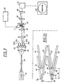
- FIG. 3 this is based on FIGS. 2a-2c explained probe array shown reduced and the Carrier structure of the probe array again with the reference symbol (1) provided.
- (22) is for optical near-field microscopy required light source, for example a laser designated.
- the light emerging from the light source (22) becomes first via an optical fiber (23) to the actual one Near field microscope. That from the optical fiber emerging light is collimated by a collimator (24) and focused by a subsequent lens array (25).
- the Lens array (25) has as many individual lenses as that Probe array (1) has individual probes. In the back focal plane of the lens array (25) is therefore one of the number of Number of foci (26a - 26d) corresponding to individual probes.
- a subsequent imaging optics (27, 28) with 5x The foci (26a - 26d) of the lens array (25) are reduced in size. reduced to the back of the probe tips of the probe array mapped and thereby coupled into the probe tips.
- the light coupled into the tip of the sod appears on the opposite side of the probe tip again and interacts with the sample (21) in a known manner. That through the sample (21) is transmitted through a light subsequent magnification optics (29) by a factor of 3 magnified to a spatially resolving detector (30) for each individual probe of the probe array (1) an independent one Has sensor surface, fed and detected by this.
- the output signals of the detector (30) are in one Video card (31) processed into a video image and subsequently displayed on a monitor (32).
- Control electronics (33) are also provided, which are connected to the probe array (1), or more precisely, with the contacts (6, 7a - 7o) of the probe array (1) and using the Capacitance of the capacitors of the individual probes Bars of the individual probes are detected and independent of each other the distance via a voltage applied to the capacitors between the individual probe tips and the surface of the Preparation (21) each regulates to a constant value.
- non-transparent preparations (21) detection of light also done in reflection.
- the detector would be (30) on the same side of the sample (21) as that Probe array (25).
- the distance between the probe tips is less than 100 ⁇ m, typically 10 to 30 ⁇ m.
- the length of the bars is on the other hand approx. 40 ⁇ m, so that the spring constant is sufficiently low of the bar and thus a sufficient sensitivity of the Deflection of the bars due to changes in the interatomic Interactions between the sample tips and the sample are measurable.
Landscapes
- Health & Medical Sciences (AREA)
- Physics & Mathematics (AREA)
- General Health & Medical Sciences (AREA)
- Radiology & Medical Imaging (AREA)
- Nuclear Medicine, Radiotherapy & Molecular Imaging (AREA)
- General Physics & Mathematics (AREA)
- Chemical & Material Sciences (AREA)
- Nanotechnology (AREA)
- Engineering & Computer Science (AREA)
- Crystallography & Structural Chemistry (AREA)
- Life Sciences & Earth Sciences (AREA)
- Optics & Photonics (AREA)
- Biophysics (AREA)
- Analytical Chemistry (AREA)
- Molecular Biology (AREA)
- Length Measuring Devices With Unspecified Measuring Means (AREA)
- Measurement Of Length, Angles, Or The Like Using Electric Or Magnetic Means (AREA)
Claims (8)
- Réseau de sondes pour un microscope à sondes à balayage comprenantcaractérisé en ceune pluralité de sondes individuelles qui sont fixées à une structure porteuse commune (1),chaque sonde individuelle présentant à chaque fois une pointe de sonde (3a - 3p) sur une ou plusieurs poutrelles (4a, 4b, 4e, 4f, 5a, 5b, 5e, 5f),les poutrelles (4a, 4b, 4e, 4f, 5a, 5b, 5e, 5f) pouvant être pliées perpendiculairement à la direction des poutrelles,les sondes individuelles étant disposées sous la forme d'une grille en deux dimensions,les directions des poutrelles (4a, 4b, 4e, 4f, 5a, 5b, 5e, 5f) contenant avec les deux directions de la grille (a, b) un angle différent de 0° ou de 180°, etles longueurs des poutrelles (4a, 4b, 4e, 4f, 5a, 5b, 5e, 5f) étant supérieures aux écarts de la grille,que les poutrelles (4a, 4b, 4e, 4f, 5a, 5b, Se, 5f) des sondes individuelles sont à chaque fois soutenues sur la structure porteuse (1) par des éléments écarteurs (9i, 9j, 9k, 9l).
- Réseau de sondes selon la revendication 1, avec lequel les poutrelles (4a, b, e, f, 5a, b, e, f) sont disposées dans un plan parallèle au plan de la structure porteuse (1).
- Réseau de sondes selon l'une des revendications 1 ou 2, avec lequel les poutrelles (4a, b, e, f, 5a, b, e, f) peuvent à chaque fois être déviées vers l'extérieur sur un trajet perpendiculaire à l'axe longitudinal des poutrelles et avec lequel la longueur des pointes des sondes (3a, 3j, 3k, 3l) est supérieure au trajet maximum de la déviation.
- Réseau de sondes selon l'une des revendications 1 à 3, avec lequel les poutrelles présentent une courbure en direction de la pointe des sondes.
- Réseau de sondes selon l'une des revendications 1 à 4, avec lequel la structure porteuse commune (1) et les poutrelles présentent à chaque fois une électrode conductrice d'électricité (6, 7a - 7p).
- Réseau de sondes selon l'une des revendications 1 à 5, avec lequel la structure porteuse présente des trous (2) associés aux pointes des sondes pour le passage de la lumière.
- Microscope à sondes à balayage équipé d'un réseau de sondes selon l'une des revendications 1 à 6.
- Microscope à sondes à balayage selon la revendication 7, avec lequel un circuit électronique de commande (29) est prévu pour commander en parallèle et indépendamment les unes des autres les électrodes des sondes individuelles pour détecter une déviation modifiée des sondes individuelles en direction des pointes des sondes.
Applications Claiming Priority (2)
| Application Number | Priority Date | Filing Date | Title |
|---|---|---|---|
| DE19701701 | 1997-01-21 | ||
| DE19701701A DE19701701A1 (de) | 1997-01-21 | 1997-01-21 | Sondenarray für ein Rastersondenmikroskop |
Publications (2)
| Publication Number | Publication Date |
|---|---|
| EP0854350A1 EP0854350A1 (fr) | 1998-07-22 |
| EP0854350B1 true EP0854350B1 (fr) | 2002-09-11 |
Family
ID=7817763
Family Applications (1)
| Application Number | Title | Priority Date | Filing Date |
|---|---|---|---|
| EP97122587A Expired - Lifetime EP0854350B1 (fr) | 1997-01-21 | 1997-12-20 | Réseau de sondes pour une sonde microscope à balayage |
Country Status (5)
| Country | Link |
|---|---|
| US (1) | US5986262A (fr) |
| EP (1) | EP0854350B1 (fr) |
| JP (1) | JPH10221350A (fr) |
| DE (2) | DE19701701A1 (fr) |
| IL (1) | IL123009A (fr) |
Cited By (1)
| Publication number | Priority date | Publication date | Assignee | Title |
|---|---|---|---|---|
| DE102010015966A1 (de) | 2010-03-15 | 2011-09-15 | Markus Hund | Quasi in situ Rastersondenmikroskop (QIS-SPM) mit einer selbsttätig betriebenen Reaktionskammer |
Families Citing this family (12)
| Publication number | Priority date | Publication date | Assignee | Title |
|---|---|---|---|---|
| US6340957B1 (en) * | 1997-08-29 | 2002-01-22 | Xerox Corporation | Dynamically relocatable tileable displays |
| US6370487B1 (en) | 1998-04-23 | 2002-04-09 | Micron Technology, Inc. | Remote semiconductor microscopy |
| JP2003501647A (ja) * | 1999-06-05 | 2003-01-14 | デーウー・エレクトロニクス・カンパニー・リミテッド | 原子間力顕微鏡及びその駆動方法 |
| JP2001091441A (ja) * | 1999-07-16 | 2001-04-06 | Japan Science & Technology Corp | ナノメートルオーダの機械振動子、その製造方法及びそれを用いた測定装置 |
| DE10003693A1 (de) | 2000-01-28 | 2001-08-02 | Zeiss Carl | Abtastsystem mit auslenkbarer Tastspitze |
| US6941823B1 (en) * | 2001-11-07 | 2005-09-13 | Veeco Instruments Inc. | Apparatus and method to compensate for stress in a microcantilever |
| EP1467948A1 (fr) * | 2002-01-24 | 2004-10-20 | Cantion A/S | Capteur |
| JP4810251B2 (ja) * | 2006-02-16 | 2011-11-09 | キヤノン株式会社 | 原子間力顕微鏡 |
| GB0621560D0 (en) * | 2006-10-31 | 2006-12-06 | Infinitesima Ltd | Probe assembly for a scanning probe microscope |
| WO2008112713A1 (fr) * | 2007-03-13 | 2008-09-18 | Nanoink, Inc. | Nanolithographie avec fenêtres de visualisation |
| US20180321276A1 (en) * | 2015-11-03 | 2018-11-08 | Board Of Regents, The University Of Texas System | Metrology devices and methods for independently controlling a plurality of sensing probes |
| US10712364B2 (en) | 2015-11-03 | 2020-07-14 | Board Of Regents, The University Of Texas Systems | Metrology devices for rapid specimen setup |
Family Cites Families (7)
| Publication number | Priority date | Publication date | Assignee | Title |
|---|---|---|---|---|
| JPH0298896A (ja) * | 1988-10-05 | 1990-04-11 | Olympus Optical Co Ltd | 記憶装置 |
| JPH02206043A (ja) * | 1989-02-03 | 1990-08-15 | Olympus Optical Co Ltd | 記憶装置 |
| US5015850A (en) * | 1989-06-20 | 1991-05-14 | The Board Of Trustees Of The Leland Stanford Junior University | Microfabricated microscope assembly |
| DE69114492T2 (de) * | 1991-09-05 | 1996-06-20 | International Business Machines Corp., Armonk, N.Y. | Einheit mit mehreren Spitzen für ein Rastertunnelmikroskop, Verfahren für deren Herstellung und Anwendung derselben in einer Speichereinheit mit direktem Zugriff. |
| JP3268797B2 (ja) * | 1991-10-09 | 2002-03-25 | オリンパス光学工業株式会社 | 光導入装置 |
| US5461907A (en) * | 1993-03-23 | 1995-10-31 | Regents Of The University Of California | Imaging, cutting, and collecting instrument and method |
| US5517280A (en) * | 1994-04-12 | 1996-05-14 | The Board Of Trustees Of The Leland Stanford, Jr. University | Photolithography system |
-
1997
- 1997-01-21 DE DE19701701A patent/DE19701701A1/de not_active Withdrawn
- 1997-12-20 EP EP97122587A patent/EP0854350B1/fr not_active Expired - Lifetime
- 1997-12-20 DE DE59708187T patent/DE59708187D1/de not_active Expired - Fee Related
-
1998
- 1998-01-16 JP JP10006445A patent/JPH10221350A/ja not_active Ceased
- 1998-01-20 IL IL12300998A patent/IL123009A/en not_active IP Right Cessation
- 1998-01-21 US US09/010,307 patent/US5986262A/en not_active Expired - Fee Related
Cited By (2)
| Publication number | Priority date | Publication date | Assignee | Title |
|---|---|---|---|---|
| DE102010015966A1 (de) | 2010-03-15 | 2011-09-15 | Markus Hund | Quasi in situ Rastersondenmikroskop (QIS-SPM) mit einer selbsttätig betriebenen Reaktionskammer |
| DE102010015966B4 (de) * | 2010-03-15 | 2014-01-30 | Markus Hund | Quasi-in-situ-Rastersondenmikroskop (QIS-SPM) mit einer selbsttätig betriebenen Reaktionskammer und Verfahren zum Betrieb |
Also Published As
| Publication number | Publication date |
|---|---|
| IL123009A (en) | 2001-12-23 |
| DE19701701A1 (de) | 1998-07-23 |
| US5986262A (en) | 1999-11-16 |
| IL123009A0 (en) | 1998-08-16 |
| DE59708187D1 (de) | 2002-10-17 |
| EP0854350A1 (fr) | 1998-07-22 |
| JPH10221350A (ja) | 1998-08-21 |
Similar Documents
| Publication | Publication Date | Title |
|---|---|---|
| DE69228681T2 (de) | Submikron Spitzenanordnung mit gegenüberliegenden Spitzen | |
| DE69618627T2 (de) | Auslegerstrukturen | |
| EP0854350B1 (fr) | Réseau de sondes pour une sonde microscope à balayage | |
| DE69227397T2 (de) | Informationsverarbeitungsvorrichtung | |
| DE60104085T2 (de) | Faseroptische schalteranordnung | |
| DE69527548T2 (de) | Apparat zur härtekontrolle durch mikroeindrückung und oberflächenabbildung mittels mehrplattenkondensatorsystem | |
| DE69226817T2 (de) | Rastertunnelmikroskop mit freitragendem Verstellungselement | |
| EP1410047B1 (fr) | Composant micromecanique | |
| DE69825226T2 (de) | Mikromechanischer XYZ-Objektträger für die Verwendung mit optischen Bauteilen | |
| DE69714334T2 (de) | Optomechanische Mikrovorrichtung und ihre optomechanischen Anwendung in einem Mikro-Strahlablenker | |
| DE19810534A1 (de) | Mehrachsenbeschleunigungssensor und Herstellungsverfahren eines Mehrachsenbeschleunigungssensor | |
| EP1030174B1 (fr) | Appareil de mesure et procédé pour sa fabrication | |
| DE10307561B4 (de) | Meßanordnung zur kombinierten Abtastung und Untersuchung von mikrotechnischen, elektrische Kontakte aufweisenden Bauelementen | |
| DE102015118394B4 (de) | Spektrometer, verfahren zur herstellung eines spektrometers und verfahren zum betreiben eines spektrometers | |
| DE102005040267A1 (de) | Verfahren zum Herstellen einer mehrschichtigen elektrostatischen Linsenanordnung | |
| EP1797568B1 (fr) | Nanomanipulateur servant a analyser ou a usiner des objets | |
| DE19531466C2 (de) | Mikromechanische Sonde für Rastermikroskope | |
| WO2000015544A1 (fr) | Ouverture pratiquee dans un materiau semi-conducteur et realisation de cette ouverture et son utilisation | |
| EP2502876B1 (fr) | Composant micromécanique doté d'une poutre en porte à faux et d'un élément électrique intégré | |
| EP0611945B1 (fr) | Microscope à force et procédé pour mesurer des forces atomiques dans plusieurs directions | |
| DE4008394C2 (de) | Verfahren und Anordnung zum Schwenken eines Lichtstrahles | |
| DE10393939T5 (de) | Schnell verfahrbare Abtastbühne für ein Rastersondenmikroskop | |
| EP1834162B1 (fr) | Composant de la technique des microsystemes, pourvu d'un dispositif deformable sous l'effet de variations de temperature | |
| DE102021200533A1 (de) | Optische Schnittstelle und Verfahren zur spektroskopischen Erfassung | |
| DE10200834A1 (de) | Abtast- und Greifvorrichtung |
Legal Events
| Date | Code | Title | Description |
|---|---|---|---|
| PUAI | Public reference made under article 153(3) epc to a published international application that has entered the european phase |
Free format text: ORIGINAL CODE: 0009012 |
|
| AK | Designated contracting states |
Kind code of ref document: A1 Designated state(s): CH DE FR GB LI SE |
|
| AX | Request for extension of the european patent |
Free format text: AL;LT;LV;MK;RO;SI |
|
| 17P | Request for examination filed |
Effective date: 19981222 |
|
| AKX | Designation fees paid |
Free format text: CH DE FR GB LI SE |
|
| RBV | Designated contracting states (corrected) |
Designated state(s): CH DE FR GB LI SE |
|
| 17Q | First examination report despatched |
Effective date: 20010206 |
|
| GRAG | Despatch of communication of intention to grant |
Free format text: ORIGINAL CODE: EPIDOS AGRA |
|
| GRAG | Despatch of communication of intention to grant |
Free format text: ORIGINAL CODE: EPIDOS AGRA |
|
| GRAH | Despatch of communication of intention to grant a patent |
Free format text: ORIGINAL CODE: EPIDOS IGRA |
|
| GRAH | Despatch of communication of intention to grant a patent |
Free format text: ORIGINAL CODE: EPIDOS IGRA |
|
| GRAA | (expected) grant |
Free format text: ORIGINAL CODE: 0009210 |
|
| AK | Designated contracting states |
Kind code of ref document: B1 Designated state(s): CH DE FR GB LI SE |
|
| PG25 | Lapsed in a contracting state [announced via postgrant information from national office to epo] |
Ref country code: GB Free format text: LAPSE BECAUSE OF FAILURE TO SUBMIT A TRANSLATION OF THE DESCRIPTION OR TO PAY THE FEE WITHIN THE PRESCRIBED TIME-LIMIT Effective date: 20020911 Ref country code: FR Free format text: LAPSE BECAUSE OF FAILURE TO SUBMIT A TRANSLATION OF THE DESCRIPTION OR TO PAY THE FEE WITHIN THE PRESCRIBED TIME-LIMIT Effective date: 20020911 |
|
| REG | Reference to a national code |
Ref country code: GB Ref legal event code: FG4D Free format text: NOT ENGLISH |
|
| REG | Reference to a national code |
Ref country code: CH Ref legal event code: EP |
|
| REF | Corresponds to: |
Ref document number: 59708187 Country of ref document: DE Date of ref document: 20021017 |
|
| PG25 | Lapsed in a contracting state [announced via postgrant information from national office to epo] |
Ref country code: SE Free format text: LAPSE BECAUSE OF FAILURE TO SUBMIT A TRANSLATION OF THE DESCRIPTION OR TO PAY THE FEE WITHIN THE PRESCRIBED TIME-LIMIT Effective date: 20021211 |
|
| GBV | Gb: ep patent (uk) treated as always having been void in accordance with gb section 77(7)/1977 [no translation filed] |
Effective date: 20020911 |
|
| EN | Fr: translation not filed | ||
| PLBE | No opposition filed within time limit |
Free format text: ORIGINAL CODE: 0009261 |
|
| STAA | Information on the status of an ep patent application or granted ep patent |
Free format text: STATUS: NO OPPOSITION FILED WITHIN TIME LIMIT |
|
| 26N | No opposition filed |
Effective date: 20030612 |
|
| PGFP | Annual fee paid to national office [announced via postgrant information from national office to epo] |
Ref country code: CH Payment date: 20081215 Year of fee payment: 12 |
|
| PGFP | Annual fee paid to national office [announced via postgrant information from national office to epo] |
Ref country code: DE Payment date: 20081219 Year of fee payment: 12 |
|
| REG | Reference to a national code |
Ref country code: CH Ref legal event code: PL |
|
| PG25 | Lapsed in a contracting state [announced via postgrant information from national office to epo] |
Ref country code: LI Free format text: LAPSE BECAUSE OF NON-PAYMENT OF DUE FEES Effective date: 20091231 Ref country code: CH Free format text: LAPSE BECAUSE OF NON-PAYMENT OF DUE FEES Effective date: 20091231 |
|
| PG25 | Lapsed in a contracting state [announced via postgrant information from national office to epo] |
Ref country code: DE Free format text: LAPSE BECAUSE OF NON-PAYMENT OF DUE FEES Effective date: 20100701 |