EP0865068A2 - Plasma Anzeigetafel - Google Patents
Plasma Anzeigetafel Download PDFInfo
- Publication number
- EP0865068A2 EP0865068A2 EP98301868A EP98301868A EP0865068A2 EP 0865068 A2 EP0865068 A2 EP 0865068A2 EP 98301868 A EP98301868 A EP 98301868A EP 98301868 A EP98301868 A EP 98301868A EP 0865068 A2 EP0865068 A2 EP 0865068A2
- Authority
- EP
- European Patent Office
- Prior art keywords
- electrodes
- display panel
- plasma display
- dielectric layer
- sets
- Prior art date
- Legal status (The legal status is an assumption and is not a legal conclusion. Google has not performed a legal analysis and makes no representation as to the accuracy of the status listed.)
- Granted
Links
Images


Classifications
-
- H—ELECTRICITY
- H01—ELECTRIC ELEMENTS
- H01J—ELECTRIC DISCHARGE TUBES OR DISCHARGE LAMPS
- H01J11/00—Gas-filled discharge tubes with alternating current induction of the discharge, e.g. alternating current plasma display panels [AC-PDP]; Gas-filled discharge tubes without any main electrode inside the vessel; Gas-filled discharge tubes with at least one main electrode outside the vessel
- H01J11/10—AC-PDPs with at least one main electrode being out of contact with the plasma
- H01J11/12—AC-PDPs with at least one main electrode being out of contact with the plasma with main electrodes provided on both sides of the discharge space
-
- H—ELECTRICITY
- H01—ELECTRIC ELEMENTS
- H01J—ELECTRIC DISCHARGE TUBES OR DISCHARGE LAMPS
- H01J11/00—Gas-filled discharge tubes with alternating current induction of the discharge, e.g. alternating current plasma display panels [AC-PDP]; Gas-filled discharge tubes without any main electrode inside the vessel; Gas-filled discharge tubes with at least one main electrode outside the vessel
- H01J11/20—Constructional details
- H01J11/22—Electrodes, e.g. special shape, material or configuration
- H01J11/32—Disposition of the electrodes
-
- H—ELECTRICITY
- H01—ELECTRIC ELEMENTS
- H01J—ELECTRIC DISCHARGE TUBES OR DISCHARGE LAMPS
- H01J11/00—Gas-filled discharge tubes with alternating current induction of the discharge, e.g. alternating current plasma display panels [AC-PDP]; Gas-filled discharge tubes without any main electrode inside the vessel; Gas-filled discharge tubes with at least one main electrode outside the vessel
- H01J11/20—Constructional details
- H01J11/34—Vessels, containers or parts thereof, e.g. substrates
- H01J11/38—Dielectric or insulating layers
-
- H—ELECTRICITY
- H01—ELECTRIC ELEMENTS
- H01J—ELECTRIC DISCHARGE TUBES OR DISCHARGE LAMPS
- H01J2211/00—Plasma display panels with alternate current induction of the discharge, e.g. AC-PDPs
- H01J2211/20—Constructional details
- H01J2211/22—Electrodes
- H01J2211/32—Disposition of the electrodes
- H01J2211/323—Mutual disposition of electrodes
Definitions
- the present invention relates to plasma display panels, and particularly to a surface-discharge type plasma display panel.
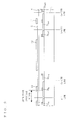
- Fig.5 is a perspective view showing a first conventional structure of a surface-discharge type plasma display panel.
- the character 1 denotes a front glass substrate as a first glass substrate.
- the characters 2x n to 2x n+2 denote x sustain discharge electrodes formed of transparent conductive film, which are provided on the front glass substrate 1.
- the characters 2y n to 2y n+1 denote y sustain discharge electrodes formed of transparent conductive film, which are provided on the front glass substrate 1.
- these x sustain discharge electrodes and the corresponding ones of the y sustain discharge electrodes are provided adjacently and in parallel with each other to form one set.
- the characters 3x n to 3x n+2 denote x bus electrodes that are laid on the x sustain discharge electrodes 2x n to 2x n+2 to supply voltage to the x sustain discharge electrodes 2x n to 2x n+2 .
- the x bus electrode 3x n supplies voltage to the x sustain discharge electrode 2x n .
- the characters 3y n to 3y n+1 denote y bus electrodes laid on the y sustain discharge electrodes 2y n to 2y n+1 for supplying voltage to the y sustain discharge electrodes 2y n to 2y n+1 .
- the y bus electrode 3y n supplies voltage to the y sustain discharge electrode 2y n .
- the x bus electrodes and the y bus electrodes in this background art, e.g., the x bus electrode 3x n and the y bus electrode 3y n are provided adjacently and in parallel with each other to form one set.
- the character 4 denotes a dielectric layer, which covers the x sustain discharge electrodes 2x n to 2x n+2 , the y sustain discharge electrodes 2y n to 2y n+1 , the x bus electrodes 3x n to 3x n+2 , and the y bus electrodes 3y n to 3y n+1 .
- the character 5 denotes a cathode film formed of magnesium oxide (hereinafter referred to as MgO), which is deposited on the dielectric layer 4 and functions as a protector and a cathode when discharging.
- the character 6 denotes a rear glass substrate as a second glass substrate, which forms a pair with the front glass substrate 1 with the dielectric layer 4 and the like therebetween.
- the character 7 denotes address electrodes, which are arranged on the rear glass substrate 6 in a direction normal to the direction in which the x sustain discharge electrodes 2x n to 2x n+2 and the y sustain discharge electrodes 2y n to 2y n+1 extend.
- a discharge space is provided between the cathode film 5 and the address electrodes 7. This discharge space is filled with mixture gas containing neon (Ne) and xenon (Xe).
- the character 8 denotes barrier ribs (hereinafter referred to as partitions), which are provided between adjacent address electrodes 7. The projecting ends of the partitions 8 are in contact with the cathode film 5 to divide the discharge space into a plurality of cells.
- the characters 9R, 9G and 9B denote red, green, and blue phosphors, respectively, which are applied on the surface of the address electrodes 7 and the side wall of partitions 8.
- the character 10 denotes discharge deactivation films, which are placed to face the spaces between the y sustain discharge electrodes and x sustain discharge electrodes in adjacent sets, e.g., the space between the y sustain discharge electrode 2y n and the x sustain discharge electrode 2x n+1 , with the dielectric layer 4 and the cathode film 5 interposed therebetween.
- This discharge deactivation films 10 are formed of an insulating material.
- the width of the discharge deactivation films 10 does not exceed the sum of the widths of a y sustain discharge electrode and an x sustain discharge electrode in adjacent sets and the width of the interval between the y sustain discharge electrode and the x sustain discharge electrode in the adjacent sets.
- Step A1 Line-Sequential Write Discharge
- the y sustain discharge electrodes 2y n to 2y n+1 are line-sequentially scanned.
- Picture signal corresponding to the image data to be outputted to the plasma display panel is outputted to the address electrodes 7 in synchronization with the line-sequential scanning.
- This causes write discharge, or the AC discharge at the intersections of the y sustain discharge electrodes 2y n to 2y n+1 and the address electrodes 7 between 2y n and 2x n , or between 2y n+1 and 2x n+1 .
- wall charge is accumulated on the surface of the cathode film 5 in the vicinities of the y sustain discharge electrodes 2y n to 2y n+1 that have made the write discharge.
- wall charge of the opposite polarity is accumulated on the surface of the cathode film 5 in the vicinities of the x sustain discharge electrodes 2x n to 2x n+1 .
- Step A2 Sustain Discharge between x and y
- the line-sequential write discharge is followed by sustain discharge, or the AC discharge for sustaining the discharge state between the y sustain discharge electrodes 2y n to 2y n+1 that have made the write discharge and the corresponding ones of the x sustain discharge electrodes 2x n to 2x n+2 , e.g., between the y sustain discharge electrode 2y n and the x sustain discharge electrode 2x n .
- Step A3 Entire-Surface Write Discharge
- a voltage required to make write discharge is applied between the opposing x sustain discharge electrodes 2x n to 2x n+2 and y sustain discharge electrodes 2y n to 2y n+1 laid on the entire surface of the front glass substrate 1.
- Step A4 Entire-Surface Erase Discharge
- Erase pulse is applied between the opposing x sustain discharge electrodes 2x n to 2x n+2 and y sustain discharge electrodes 2y n to 2y n+1 laid on the entire surface of the front glass substrate 1 to erase wall charge unwanted in the next driving sequence A1.
- the phosphor 9R receives ultra-violet rays emitted in the process of discharge to emit fluorescent red color. Similarly, the phosphor 9G emits green color and the phosphor 9B emits blue color.
- Fig.6 is a sectional view of the conventional surface-discharge type plasma display panel shown in Fig.5. This sectional view of the plasma display panel in Fig.6 does not show the rear glass substrate 6, the address electrodes 7, the partitions 8 and the phosphors 9R, 9G and 9B. This technique is disclosed in Japanese Patent Laying-Open No.9-102280, for example.
- Fig.7 is a sectional view showing a second conventional structure of a surface-discharge type plasma display panel.
- the same reference characters as those in the conventional example shown in Fig.5 and Fig.6 show the same or corresponding parts, which are not described here again.
- one x sustain discharge electrode e.g., the x sustain discharge electrode 2x m
- two y sustain discharge electrodes e.g., between the y sustain discharge electrode 2y n and the y sustain discharge electrode 2y n+1 .
- the plasma display panel of the second structure has nothing corresponding to the discharge deactivation films 10 provided in the plasma display panel of the first structure.
- the erroneous discharge between adjacent bus electrodes in different sets can be prevented by forming the discharge deactivation films 10 in positions facing the spaces between, e.g., the y bus electrode 3y n-1 and the x bus electrode 3x n through the dielectric layer 4 and the cathode film 5.
- the plasma display panel of the second structure corresponds to an improvement of the plasma display panel of the first structure made to decrease the total number of the x bus electrodes and y bus electrodes provided on the front glass substrate having a given number of cells by allowing two y bus electrodes to share one x bus electrode so that the facing x and y bus electrodes can be spaced at increased gaps to improve the light emission luminance for comfortable-to-see display.
- the wall charge accumulated before that on the cathode film 5 in the region above the x sustain discharge electrode 2x m is uniformly reduced. Then the rise of discharge occurring thereafter between the y sustain discharge electrode 2y n+1 sharing the x sustain discharge electrode 2x m with the y sustain discharge electrode 2y n and the x sustain discharge electrode 2x m will be especially unstable.
- the x sustain discharge electrode 2x m and the y sustain discharge electrode 2y n-1 are prone to erroneously make discharge, involved in the discharge between the x sustain discharge electrode 2x m and the y sustain discharge electrode 2y n .
- a plasma display panel comprises: a first glass substrate and a second glass substrate facing each other; a plurality of sets of discharge sustain electrodes, each set including one common electrode and two independent electrodes on both sides of the common electrode, provided on a surface of the first glass substrate that faces the second glass substrate, the common electrode and the two independent electrodes extending in parallel with each other; a dielectric layer coating the plurality of sets of discharge sustain electrodes; a plurality of address electrodes provided in parallel in a direction perpendicular to the common electrodes on a surface of the second glass substrate that faces the first glass substrate with a space interposed between the dielectric layer and the address electrodes; partitions provided between adjacent ones of the address electrodes between the first and second glass substrates; a phosphor coating the partitions; and first insulating parts provided in positions facing the common electrodes with the dielectric layer interposed therebetween.
- a reduced number of discharge sustain electrodes are provided on the first glass substrate, which allows bus electrodes included in the opposing common electrodes and the bus electrodes included in independent electrodes to be spaced at increased intervals, thus improving the light emission luminance of the plasma display panel.
- the formation of the insulating part in a position facing the common electrode through the dielectric layer sustains the wall charge on the side of the other independent electrode provided on the other side of the common electrode in the same set, enabling the independent electrodes in the same set of discharge sustain electrodes to stably discharge.
- the plasma display panel according to the present invention further comprises second insulating parts provided in positions facing positions between adjacent ones of the independent electrodes in adjacent ones of the plurality of discharge sustain electrode sets with the dielectric layer interposed therebetween.
- the first and second insulating parts are formed of such an insulating material that the firing voltage between the independent electrodes and the common electrodes in the presence of the first or second insulating parts is higher than the firing voltage between the independent electrodes and the common electrodes in the presence of only a cathode film provided on the dielectric layer.
- the first and second insulating parts are formed by depositing the insulating material on the dielectric layer or the cathode film while evaporating the insulating material.
- the insulating material is Al 2 O 3 or TiO 2 .
- the plasma display panel according to the present invention further comprises independent parts formed of a material having a light-shielding property and provided on the first glass substrate between adjacent ones of the independent electrodes in adjacent ones of the plurality of discharge sustain electrode sets.
- the independent parts are formed of the same material as the independent electrodes.
- the independent parts and the independent electrodes can be easily formed by using pattern design of photomask used in the same photolithography.
- the independent parts can thus be easily formed without adding any new process for formation of the independent parts.
- the material of the independent parts is chromium.
- chromium Since chromium has dark metallic luster and a high light-shielding property, it improves the visual contrast of the plasma display panel.
- the present invention has been made to solve the above-described problems, and an object of the present invention is to provide a plasma display panel that prevents the problem that when discharge starts between the y sustain discharge electrode 2y n and the x sustain discharge electrode 2x m , for example, wall charge accumulated before that on the cathode film 5 in the region above the x sustain discharge electrode 2x m is uniformly reduced, so that the discharge made thereafter between the y sustain discharge electrode 2y n+1 sharing the x sustain discharge electrode 2x m with the y sustain discharge electrode 2y n and the x sustain discharge electrode 2x m can rise in a stable manner.
- Another object of the present invention is to provide a surface-discharge type plasma display panel that can prevent occurrence of erroneous discharge caused between an x bus electrode in a certain set and a y bus electrode in a set adjacent to the set including the x bus electrode.
- Fig.1 is a sectional view showing a plasma display panel of a first preferred embodiment of the present invention.
- Fig.2 is a sectional view showing a plasma display panel of a second preferred embodiment of the present invention.
- Fig.3 is a sectional view showing a plasma display panel of a third preferred embodiment of the present invention.
- Fig.4 is a sectional view showing a plasma display panel that does not have the y discharge deactivation films described in the third preferred embodiment of the present invention.
- Fig.5 is a perspective view showing a plasma display panel of a background art.
- Fig.6 is a sectional view showing the plasma display panel of the background art.
- Fig.7 is a sectional view showing a plasma display panel of a background art.
- Fig.1 is a sectional view showing the plasma display panel.
- the same reference characters as those in the examples of background art show the same or corresponding parts and those parts are not described here again.
- the embodiment will be described in respect of the differences.
- the rear glass substrate 6, the address electrodes 7, the partitions 8 and the phosphors 9R, 9G, 9B have the same structures as those in Fig.5.
- the x sustain discharge electrodes 2x m-1 to 2x m+1 and y sustain discharge electrodes 2y n-2 to 2y n+3 are arranged in the following order in the first preferred embodiment: y sustain discharge electrode 2y n-2 , x sustain discharge electrode 2x m- 1 , y sustain discharge electrode 2y n-1 , y sustain discharge electrode 2y n , x sustain discharge electrode 2x m , y sustain discharge electrode 2y n+1 , y sustain discharge electrode 2y n+2 , x sustain discharge electrode 2x m+1 and y sustain discharge electrode 2y n+3 . They extend perpendicular to the direction in which the address electrodes 7 shown in Fig.5 extend.
- One x sustain discharge electrode e.g., the x sustain discharge electrode 2x m makes discharge on the nth line with the y sustain discharge electrode 2y n and on the (n+1)th line with the y sustain discharge electrode 2y n+1 .
- the character 11 denotes insulating parts serving as x discharge deactivation films, which are provided in positions facing the common electrodes or x bus electrodes 3x m-1 to 3x m+1 through the dielectric layer 4 and the cathode layer 5.
- the character 12 denotes insulating parts serving as y discharge deactivation films, which are provided in positions facing the spaces between two adjacent independent electrodes or y bus electrodes, e.g., the space between the y bus electrode 3y n and the y bus electrode 3y n-1 , through the dielectric layer 4 and the cathode layer 5.
- One x bus electrode and two y bus electrodes on its both sides form one set of discharge sustain electrodes.
- the width of the y discharge deactivation films 12 does not exceed the sum of the widths of two y bus electrodes in adjacent sets, e.g., the widths of the y bus electrode 3y n and the y bus electrode 3y n-1, and the width of the space between the two y sustain discharge electrodes in the adjacent sets.
- the spacing between adjacent two y sustain discharge electrodes in adjacent sets e.g., the spacing between the y sustain discharge electrode 2y n-1 and the y sustain discharge electrode 2y n is sufficiently large, it is not particularly necessary to provide the y discharge deactivation films 12 shown in the first preferred embodiment.
- the cathode film 5 is laid on the dielectric layer 4 and the x and y discharge deactivation films 11 to 12 are patterned thereon.
- the x and y discharge deactivation films 11 to 12 may be laid plainly on the dielectric layer 4 and then the cathode film 5 may be patterned thereon in the negative shape of the x and y discharge deactivation film 11 to 12 shown in Fig. 1.
- one x bus electrode 3x m-1 (or 3x m ; 3x m+1 ) is interposed and shared between two y bus electrodes 3y n-2 , 3y n-1 (or 3y n , 3y n+1 ; 3y n+2 , 3y n+3 ). Accordingly, when the same number of cells are formed on a plasma display panel having the same space as those in conventional ones, a reduced total number of x bus electrodes 3x m-1 to 3x m+1 and y bus electrodes 3y n-2 to 3y n+3 are formed on the front glass substrate 1. Then opposing x bus electrodes and y bus electrodes, e.g., the x bus electrode 3x m and the y bus electrode 3y n , can be provided at larger gaps, thus improving the light emission luminance of the plasma display panel.
- opposing x bus electrodes and y bus electrodes e.g., the x bus electrode 3x m and the y bus electrode
- the plasma display panel of the first preferred embodiment has the y discharge deactivation films 12 provided in the vicinities of the boundaries between adjacent sets of electrodes, e.g., in the position facing the interval between the adjacent y bus electrodes 3y n-1 and 3y n through the dielectric layer 4 and the cathode film 5, the flow of discharge current is controlled.
- the x sustain discharge electrode 2x m and the y sustain discharge electrode 2y n-1 are prevented from being involved in discharge between the x sustain discharge electrode 2x m and the y sustain discharge electrode 2y n to erroneously discharge.
- the plasma display panel of the first preferred embodiment has the x discharge deactivation films 11 in positions facing the x bus electrodes 3x m-1 to 3x m+1 through the dielectric layer 4 and the cathode film 5. This prevents the problem that, for example, the wall charge to be held between the x sustain discharge electrode 2x m and the y sustain discharge electrode 2y n+1 is lost, involved in the discharge between the x sustain discharge electrode 2x m and the y sustain discharge electrode 2y n . This allows the x sustain discharge electrode 2x m and the y sustain discharge electrode 2y n+1 to stably discharge even after discharge has been started between the x sustain discharge electrode 2x m and the y sustain discharge electrode 2y n .
- the spacing between two adjacent y sustain discharge electrodes in adjacent sets e.g., the spacing between the y sustain discharge electrode 2y n+1 and the y sustain discharge electrode 2y n+2 , is sufficiently larger than in the first preferred embodiment.
- a pattern of y discharge deactivation films 12 having a light-shielding property is formed in the positions facing the spaces between adjacent y sustain discharge electrodes, e.g., the space between the y sustain discharge electrode 2y n+1 and the y sustain discharge electrode 2y n+2 , through the dielectric layer 4 and the cathode film 5.
- the formation of the light-shielding y discharge deactivation films 12 prevents, to some extent, the problem that the white base of the phosphors 9R, 9G and 9B is seen through the spaces between adjacent two y sustain discharge electrodes in adjacent sets in the plasma display panel, thus improving the visual contrast of the plasma display panel.
- the y discharge deactivation films 12 having a light-shielding property can be formed by bringing an insulating material for the y discharge deactivation films 12, e.g., aluminum oxide (hereinafter referred to as Al 2 O 3 ) or titanium oxide (hereinafter referred to as TiO 2 ), to an oxygen-lacking state from the stoichiometric composition. This utilizes the phenomenon that these oxides present blacker tone with lack of oxygen.
- Al 2 O 3 aluminum oxide
- TiO 2 titanium oxide
- the y discharge deactivation films 12 containing oxygen-lacking oxide are formed by depositing a sample of Al 2 O 3 or TiO 2 on the cathode film 5 while evaporating the sample with stoichiometric composition to decompose and eliminate part of oxygen.
- the y discharge deactivation films 12 formed of Al 2 O 3 or TiO 2 have higher discharge voltage than the y discharge deactivation films 12 formed of MgO. Table 1 shows results of experiment showing this.
- the plasma display panel of the second preferred embodiment has a pattern of y discharge deactivation films 12 having a light-shielding property laid in positions facing the spaces between adjacent y sustain discharge electrodes, e.g., the space between the y sustain discharge electrode 2y n+1 and the y sustain discharge electrode 2y n+2 , with the dielectric layer 4 and the cathode film 5 interposed therebetween.
- the formation of the y discharge deactivation films 12 having a light-shielding property prevents, to some extent, the problem that the white base of the phosphors 9R, 9G and 9B is seen through the spaces between adjacent two y sustain discharge electrodes in adjacent sets in the plasma display panel, thus improving the visual contrast of the plasma display panel.
- the spacing between two adjacent y sustain discharge electrodes in adjacent sets e.g., the space between the y sustain discharge electrode 2y n+1 and the y sustain discharge electrode 2y n+2 , is sufficiently large.
- metal shadow patterns 13 are provided as independent parts formed of the same material as the x bus electrodes 3x m to 3x m+1 and the y bus electrodes 3y n to 3y n+3 in the spaces between adjacent two y sustain discharge electrodes in adjacent sets shown in the second preferred embodiment, e.g., in the space between the y sustain discharge electrode 2y n+1 and the y sustain discharge electrode 2y n+2 .
- the metal shadow patterns 13 are applied no external voltage, or floating.
- the x bus electrodes 3x m to 3x m+1 and the y bus electrodes 3y n to 3y n+3 are formed of multi-layered film composed of chromium (Cr), copper (Cu) and Cr films, or multi-layered film composed of aluminum (Al) and Cr films. These multi-layered films have perfect light-shielding property. Especially, seen in many plasma display panels is the Cr film having dark metallic luster and a high light-shielding property.
- a multi-layered film formed of Cr film is provided as the shadow pattern 13 in the space between the y sustain discharge electrode 2y n+1 and the y sustain discharge electrode 2y n+2 , for example, it prevents the white base of the phosphors 9R, 9G and 9B from being seen through the space between the two adjacent y sustain discharge electrodes in adjacent sets in the plasma display panel, thus improving the visual contrast of the plasma display panel.
- the shadow patterns 13 can be easily formed by using the pattern design of photomask used in photolithography for the x bus electrodes and y bus electrodes. Accordingly, it is not necessary to add a new process for formation of the shadow patterns 13.
- Fig.4 is a sectional view showing a structure of a plasma display panel having the metal shadow patterns 13 without a pattern of y discharge deactivation films 12 in the positions facing the spaces between two adjacent y sustain discharge electrodes in adjacent sets, e.g., the space between the y sustain discharge electrode 2y n+1 and the y sustain discharge electrode 2y n+2 with the dielectric layer 4 and the cathode film 5 interposed therebetween.
- discharge made between the x sustain discharge electrode 2x m and the y sustain discharge electrode 2y n+1 for example, accumulates wall charge on the cathode film 5 facing the metal shadow pattern 13 through the dielectric layer 4, which causes spark discharge at certain instant.
- the plasma display panel of the third preferred embodiment has the metal shadow patterns 13 having a light-shielding property and formed of the same material as the x bus electrodes 3x m to 3 m+1 and the y bus electrodes 3y n to 3y n+2 in the intervals between two adjacent y sustain discharge electrodes in adjacent sets, e.g., in the space between the y sustain discharge electrode 2y n+1 and the y sustain discharge electrode 2y n+2 .
- the plasma display panel of the third preferred embodiment reduces the risk of occurrence of spark discharge.
Landscapes
- Engineering & Computer Science (AREA)
- Physics & Mathematics (AREA)
- Plasma & Fusion (AREA)
- Chemical & Material Sciences (AREA)
- Materials Engineering (AREA)
- Gas-Filled Discharge Tubes (AREA)
Priority Applications (1)
| Application Number | Priority Date | Filing Date | Title |
|---|---|---|---|
| EP03012506A EP1351270A3 (de) | 1997-03-14 | 1998-03-12 | Plasmaanzeigetafel |
Applications Claiming Priority (3)
| Application Number | Priority Date | Filing Date | Title |
|---|---|---|---|
| JP60930/97 | 1997-03-14 | ||
| JP6093097 | 1997-03-14 | ||
| JP06093097A JP3588961B2 (ja) | 1997-03-14 | 1997-03-14 | プラズマディスプレイパネル |
Related Child Applications (1)
| Application Number | Title | Priority Date | Filing Date |
|---|---|---|---|
| EP03012506A Division EP1351270A3 (de) | 1997-03-14 | 1998-03-12 | Plasmaanzeigetafel |
Publications (3)
| Publication Number | Publication Date |
|---|---|
| EP0865068A2 true EP0865068A2 (de) | 1998-09-16 |
| EP0865068A3 EP0865068A3 (de) | 1999-04-07 |
| EP0865068B1 EP0865068B1 (de) | 2004-05-12 |
Family
ID=13156604
Family Applications (2)
| Application Number | Title | Priority Date | Filing Date |
|---|---|---|---|
| EP03012506A Withdrawn EP1351270A3 (de) | 1997-03-14 | 1998-03-12 | Plasmaanzeigetafel |
| EP98301868A Expired - Lifetime EP0865068B1 (de) | 1997-03-14 | 1998-03-12 | Plasma Anzeigetafel |
Family Applications Before (1)
| Application Number | Title | Priority Date | Filing Date |
|---|---|---|---|
| EP03012506A Withdrawn EP1351270A3 (de) | 1997-03-14 | 1998-03-12 | Plasmaanzeigetafel |
Country Status (5)
| Country | Link |
|---|---|
| US (1) | US6137226A (de) |
| EP (2) | EP1351270A3 (de) |
| JP (1) | JP3588961B2 (de) |
| KR (1) | KR19980080061A (de) |
| DE (1) | DE69823724T2 (de) |
Cited By (2)
| Publication number | Priority date | Publication date | Assignee | Title |
|---|---|---|---|---|
| EP1041599A3 (de) * | 1999-03-31 | 2000-11-22 | Matsushita Electric Industrial Co., Ltd. | Wechselstrom Plasmaanzeigetafel |
| EP1306873B1 (de) * | 2001-10-26 | 2006-12-27 | Mitsubishi Denki Kabushiki Kaisha | Plasmabildschirm und Plasmaanzeigevorrichtung |
Families Citing this family (21)
| Publication number | Priority date | Publication date | Assignee | Title |
|---|---|---|---|---|
| JP3163563B2 (ja) * | 1995-08-25 | 2001-05-08 | 富士通株式会社 | 面放電型プラズマ・ディスプレイ・パネル及びその製造方法 |
| KR100516122B1 (ko) * | 1998-01-26 | 2005-12-29 | 엘지전자 주식회사 | 플라즈마 표시장치의 유지전극구조 |
| KR100412035B1 (ko) * | 1998-12-16 | 2003-12-24 | 주식회사 삼우기초기술 | 인장재 정착 및 제거형 그라운드 앵커 |
| JP3589892B2 (ja) * | 1999-03-18 | 2004-11-17 | 富士通株式会社 | プラズマディスプレイパネル |
| KR100432998B1 (ko) * | 1999-07-09 | 2004-05-24 | 삼성에스디아이 주식회사 | 플라즈마 디스플레이 패널 |
| JP4331359B2 (ja) | 1999-11-18 | 2009-09-16 | 三菱電機株式会社 | 交流型プラズマディスプレイパネルの駆動方法 |
| KR100373532B1 (ko) * | 2001-01-18 | 2003-02-25 | 엘지전자 주식회사 | 플라즈마 디스플레이 패널의 구동방법 |
| DE69924121T2 (de) * | 1999-12-16 | 2006-04-27 | Ferro Gmbh | Emaillezusammensetzung für dielektrische Schichten, darin enthaltene weisse Pigmente mit verbesserter Benetzbarkeit und Plasmaanzeigetafel mit der dielektrischen Schicht |
| JP2002056775A (ja) | 2000-06-02 | 2002-02-22 | Mitsubishi Electric Corp | プラズマディスプレイパネル用基板の製造方法、プラズマディスプレイパネル用基板及びプラズマディスプレイパネル |
| KR100389020B1 (ko) * | 2000-11-24 | 2003-06-25 | 엘지전자 주식회사 | 플라즈마 디스플레이 패널 |
| JP4527862B2 (ja) * | 2000-09-04 | 2010-08-18 | 日立プラズマディスプレイ株式会社 | プラズマディスプレイパネル |
| JP3688206B2 (ja) * | 2001-02-07 | 2005-08-24 | 富士通日立プラズマディスプレイ株式会社 | プラズマディスプレイパネルの駆動方法および表示装置 |
| KR100389025B1 (ko) * | 2001-07-18 | 2003-06-25 | 엘지전자 주식회사 | 플라즈마 디스플레이 패널 |
| KR100421489B1 (ko) * | 2001-09-28 | 2004-03-11 | 엘지전자 주식회사 | 플라즈마 디스플레이 패널 |
| EP1361594A3 (de) | 2002-05-09 | 2005-08-31 | Lg Electronics Inc. | Plasma Anzeigetafel |
| JP2004335280A (ja) * | 2003-05-08 | 2004-11-25 | Pioneer Electronic Corp | プラズマディスプレイパネル |
| KR100769191B1 (ko) * | 2004-03-22 | 2007-10-23 | 엘지.필립스 엘시디 주식회사 | 평판 발광 램프 장치 및 그 제조방법 |
| KR100667931B1 (ko) * | 2004-11-15 | 2007-01-11 | 삼성에스디아이 주식회사 | 플라즈마 디스플레이 패널 |
| KR100708709B1 (ko) * | 2005-08-06 | 2007-04-17 | 삼성에스디아이 주식회사 | 플라즈마 디스플레이 패널 |
| WO2009011067A1 (ja) * | 2007-07-19 | 2009-01-22 | Hitachi, Ltd. | プラズマディスプレイパネル及びその製造方法 |
| JP4951479B2 (ja) | 2007-12-06 | 2012-06-13 | 株式会社日立製作所 | プラズマディスプレイパネル |
Family Cites Families (16)
| Publication number | Priority date | Publication date | Assignee | Title |
|---|---|---|---|---|
| JPS6047341A (ja) * | 1983-08-24 | 1985-03-14 | Fujitsu Ltd | ガス放電パネル |
| JP2629944B2 (ja) * | 1989-02-20 | 1997-07-16 | 富士通株式会社 | ガス放電パネルとその駆動方法 |
| JP2803131B2 (ja) * | 1989-02-23 | 1998-09-24 | 日本電気株式会社 | 面放電型ドットマトリクスパネル |
| JP2964512B2 (ja) * | 1989-12-18 | 1999-10-18 | 日本電気株式会社 | カラープラズマディスプレイ |
| JP3115927B2 (ja) * | 1992-01-10 | 2000-12-11 | 富士通株式会社 | 表示装置 |
| EP0554172B1 (de) * | 1992-01-28 | 1998-04-29 | Fujitsu Limited | Plasma Farbanzeige-Vorrichtung von Oberflächenentladungs-Typ |
| JP3484715B2 (ja) * | 1993-03-17 | 2004-01-06 | 富士通株式会社 | プラズマディスプレイパネル |
| JP3394799B2 (ja) * | 1993-09-13 | 2003-04-07 | パイオニア株式会社 | プラズマディスプレイ装置 |
| JP3511667B2 (ja) * | 1994-03-18 | 2004-03-29 | 富士通株式会社 | 面放電型ガス放電パネル |
| US5818168A (en) * | 1994-09-07 | 1998-10-06 | Hitachi, Ltd. | Gas discharge display panel having communicable main and auxiliary discharge spaces and manufacturing method therefor |
| JP3224486B2 (ja) * | 1995-03-15 | 2001-10-29 | パイオニア株式会社 | 面放電型プラズマディスプレイパネル |
| JP2848278B2 (ja) * | 1995-07-14 | 1999-01-20 | 日本電気株式会社 | カラープラズマディスプレイパネルおよびその製造方法 |
| US6373452B1 (en) * | 1995-08-03 | 2002-04-16 | Fujiitsu Limited | Plasma display panel, method of driving same and plasma display apparatus |
| JP3163563B2 (ja) * | 1995-08-25 | 2001-05-08 | 富士通株式会社 | 面放電型プラズマ・ディスプレイ・パネル及びその製造方法 |
| US5872425A (en) * | 1995-08-31 | 1999-02-16 | Matsushita Electronics Corporation | Plasma display device and method for driving the same |
| JP3674107B2 (ja) * | 1995-10-03 | 2005-07-20 | 三菱電機株式会社 | 面放電型ac型プラズマディスプレイパネル |
-
1997
- 1997-03-14 JP JP06093097A patent/JP3588961B2/ja not_active Expired - Fee Related
-
1998
- 1998-03-10 KR KR1019980007837A patent/KR19980080061A/ko not_active Ceased
- 1998-03-12 EP EP03012506A patent/EP1351270A3/de not_active Withdrawn
- 1998-03-12 EP EP98301868A patent/EP0865068B1/de not_active Expired - Lifetime
- 1998-03-12 DE DE69823724T patent/DE69823724T2/de not_active Expired - Fee Related
- 1998-03-13 US US09/041,730 patent/US6137226A/en not_active Expired - Fee Related
Cited By (3)
| Publication number | Priority date | Publication date | Assignee | Title |
|---|---|---|---|---|
| EP1041599A3 (de) * | 1999-03-31 | 2000-11-22 | Matsushita Electric Industrial Co., Ltd. | Wechselstrom Plasmaanzeigetafel |
| US6545405B1 (en) | 1999-03-31 | 2003-04-08 | Matsushita Electric Industrial Co., Ltd. | AC plasma display panel having scanning/sustain electrodes of particular structure |
| EP1306873B1 (de) * | 2001-10-26 | 2006-12-27 | Mitsubishi Denki Kabushiki Kaisha | Plasmabildschirm und Plasmaanzeigevorrichtung |
Also Published As
| Publication number | Publication date |
|---|---|
| EP0865068B1 (de) | 2004-05-12 |
| JP3588961B2 (ja) | 2004-11-17 |
| EP1351270A2 (de) | 2003-10-08 |
| US6137226A (en) | 2000-10-24 |
| DE69823724D1 (de) | 2004-06-17 |
| DE69823724T2 (de) | 2005-05-04 |
| JPH10255664A (ja) | 1998-09-25 |
| EP0865068A3 (de) | 1999-04-07 |
| EP1351270A3 (de) | 2007-03-07 |
| KR19980080061A (ko) | 1998-11-25 |
Similar Documents
| Publication | Publication Date | Title |
|---|---|---|
| EP0865068B1 (de) | Plasma Anzeigetafel | |
| JP2000082407A (ja) | プラズマディスプレイパネル | |
| JPH05266800A (ja) | 面放電型プラズマディスプレイパネル | |
| JP3674107B2 (ja) | 面放電型ac型プラズマディスプレイパネル | |
| JPH04264330A (ja) | プラズマ表示素子とその製造方法 | |
| KR100366099B1 (ko) | 격벽의 폭이 다르게 형성된 플라즈마 디스플레이 패널 | |
| JP2000243299A (ja) | プラズマディスプレイパネル | |
| JP3423742B2 (ja) | 面放電型プラズマディスプレイパネル | |
| KR100351846B1 (ko) | 플라즈마 디스플레이 패널 | |
| JPH09129140A (ja) | 面放電型プラズマディスプレイパネル | |
| JP2964717B2 (ja) | プラズマディスプレイパネル | |
| JP3097635B2 (ja) | プラズマディスプレイパネルとその駆動方法 | |
| JPH05234520A (ja) | Ac面放電型プラズマディスプレイパネル | |
| EP1632977B1 (de) | Plasmaanzeigetafel | |
| KR100367762B1 (ko) | 플라즈마 디스플레이 패널 | |
| JP2003142006A (ja) | プラズマディスプレイパネルおよびその製造方法 | |
| US7400092B2 (en) | Plasma display having barrier ribs that each overlap the bus electrodes of different electrodes only in part | |
| EP1601000A1 (de) | Plasmaanzeigetafel | |
| US20050148151A1 (en) | Plasma display panel and manufacturing method thereof | |
| JPH09330665A (ja) | Ac型プラズマディスプレイパネル | |
| US20060145613A1 (en) | Plasma display apparatus | |
| KR100515844B1 (ko) | 복수의 보호층을 구비하는 플라즈마 디스플레이 패널 | |
| KR100658315B1 (ko) | 스캔 전극과 서스테인 전극을 포함하는 플라즈마디스플레이 패널 | |
| US7595591B2 (en) | Plasma display panel | |
| US20060097638A1 (en) | Plasma display panel |
Legal Events
| Date | Code | Title | Description |
|---|---|---|---|
| PUAI | Public reference made under article 153(3) epc to a published international application that has entered the european phase |
Free format text: ORIGINAL CODE: 0009012 |
|
| AK | Designated contracting states |
Kind code of ref document: A2 Designated state(s): DE FR GB |
|
| AX | Request for extension of the european patent |
Free format text: AL;LT;LV;MK;RO;SI |
|
| PUAL | Search report despatched |
Free format text: ORIGINAL CODE: 0009013 |
|
| AK | Designated contracting states |
Kind code of ref document: A3 Designated state(s): AT BE CH DE DK ES FI FR GB GR IE IT LI LU MC NL PT SE |
|
| AX | Request for extension of the european patent |
Free format text: AL;LT;LV;MK;RO;SI |
|
| 17P | Request for examination filed |
Effective date: 19990505 |
|
| AKX | Designation fees paid |
Free format text: DE FR GB |
|
| 17Q | First examination report despatched |
Effective date: 20010530 |
|
| GRAP | Despatch of communication of intention to grant a patent |
Free format text: ORIGINAL CODE: EPIDOSNIGR1 |
|
| GRAS | Grant fee paid |
Free format text: ORIGINAL CODE: EPIDOSNIGR3 |
|
| GRAA | (expected) grant |
Free format text: ORIGINAL CODE: 0009210 |
|
| AK | Designated contracting states |
Kind code of ref document: B1 Designated state(s): DE FR GB |
|
| REG | Reference to a national code |
Ref country code: GB Ref legal event code: FG4D |
|
| REF | Corresponds to: |
Ref document number: 69823724 Country of ref document: DE Date of ref document: 20040617 Kind code of ref document: P |
|
| ET | Fr: translation filed | ||
| PLBE | No opposition filed within time limit |
Free format text: ORIGINAL CODE: 0009261 |
|
| STAA | Information on the status of an ep patent application or granted ep patent |
Free format text: STATUS: NO OPPOSITION FILED WITHIN TIME LIMIT |
|
| 26N | No opposition filed |
Effective date: 20050215 |
|
| PGFP | Annual fee paid to national office [announced via postgrant information from national office to epo] |
Ref country code: GB Payment date: 20090311 Year of fee payment: 12 |
|
| PGFP | Annual fee paid to national office [announced via postgrant information from national office to epo] |
Ref country code: DE Payment date: 20090306 Year of fee payment: 12 |
|
| PGFP | Annual fee paid to national office [announced via postgrant information from national office to epo] |
Ref country code: FR Payment date: 20090316 Year of fee payment: 12 |
|
| GBPC | Gb: european patent ceased through non-payment of renewal fee |
Effective date: 20100312 |
|
| REG | Reference to a national code |
Ref country code: FR Ref legal event code: ST Effective date: 20101130 |
|
| PG25 | Lapsed in a contracting state [announced via postgrant information from national office to epo] |
Ref country code: FR Free format text: LAPSE BECAUSE OF NON-PAYMENT OF DUE FEES Effective date: 20100331 |
|
| PG25 | Lapsed in a contracting state [announced via postgrant information from national office to epo] |
Ref country code: DE Free format text: LAPSE BECAUSE OF NON-PAYMENT OF DUE FEES Effective date: 20101001 |
|
| PG25 | Lapsed in a contracting state [announced via postgrant information from national office to epo] |
Ref country code: GB Free format text: LAPSE BECAUSE OF NON-PAYMENT OF DUE FEES Effective date: 20100312 |