EP0866378A2 - Röntgenbildlöschvorrichtung - Google Patents
Röntgenbildlöschvorrichtung Download PDFInfo
- Publication number
- EP0866378A2 EP0866378A2 EP98301570A EP98301570A EP0866378A2 EP 0866378 A2 EP0866378 A2 EP 0866378A2 EP 98301570 A EP98301570 A EP 98301570A EP 98301570 A EP98301570 A EP 98301570A EP 0866378 A2 EP0866378 A2 EP 0866378A2
- Authority
- EP
- European Patent Office
- Prior art keywords
- erasure
- high voltage
- voltage
- light
- charges
- Prior art date
- Legal status (The legal status is an assumption and is not a legal conclusion. Google has not performed a legal analysis and makes no representation as to the accuracy of the status listed.)
- Granted
Links
Images


Classifications
-
- G—PHYSICS
- G03—PHOTOGRAPHY; CINEMATOGRAPHY; ANALOGOUS TECHNIQUES USING WAVES OTHER THAN OPTICAL WAVES; ELECTROGRAPHY; HOLOGRAPHY
- G03G—ELECTROGRAPHY; ELECTROPHOTOGRAPHY; MAGNETOGRAPHY
- G03G13/00—Electrographic processes using a charge pattern
- G03G13/054—Electrographic processes using a charge pattern using X-rays, e.g. electroradiography
Definitions
- This invention relates to a method of erasure of x-ray images.
- a method of erasure of an x-ray imaging device which uses high bias voltage during the image capture process, which comprises simultaneously applying high voltage and light to the device so as to erase a previous image on said device.
- Such a method of erasure of an x-ray imaging device can completely or essentially completely eliminate non-uniformities or ghosts arising from a previous image.
- erasure of an x-ray imaging device where a previous image has been obtained with application of a high voltage bias during the imaging process, can be significantly improved by also applying a high voltage bias to the x-ray imaging device when exposing the device to erasing light. Once erasure is complete, the high voltage is turned off before turning off the light. It is preferable, although not essential, to use the same magnitude of high voltage bias during imaging as during erasure.
- the x-ray imaging device that may be treated in accordance with the novel process will normally comprise a plate of a photoconductive material overcoated with a layer of a dielectric material.
- the photoconductive material may, for example, be amorphous selenium, lead oxide, cadmium sulphide, cadmium telluride, thallium bromide, mercuric iodide or similar materials which are suitable for x-ray imaging while applying high voltage bias.
- the dielectric material may be any suitable dielectric for such purposes, for example, parylene, polycarbonate, polyester and the like.
- the x-ray imaging device is provided with a substrate on which the photoconductive plate is mounted.
- Such substrate may consist of any suitable material such as aluminum, ITO coated glass, a thin film transistor array (TFT), and the like.
- a thin layer of a conductive material which acts as the biasing electrode it may be selected from gold, platinum, aluminum, chromium, indium tin oxide (ITO) or the like.
- an x-ray imaging device such as described above is used for imaging, it is normally positively biased and charges (electron-hole pairs) that are generated from x-ray absorbtion by the photoconductor will move under the applied electric field. Negative charges will move in the direction of the top positive electrode and will stop and accumulate at the photoconductor-dielectric interface. When erasure of such device takes place for subsequent re-use, a ghost will usually remain due to a non-uniform charge accumulation at the interface between the photoconductive plate and the dielectric layer. This non-uniform charge accumulation causes a non-uniform sensitivity within the x-ray imaging device that produces the ghost.
- One way to eliminate such non-uniformity and ghosts is by uniformizing the charges at the interface. This is achieved by subjecting the x-ray imaging device simultaneously to a positive high voltage and to an erasing light and then turning off the voltage and thereafter the light. The sensitivity of the plate will be somewhat lower with this operation, but it will be uniform within the plate, allowing for the elimination of the ghosts.
- the negative charges at the interface can completely or essentially completely eliminate the negative charges at the interface by switching the high voltage from positive to negative polarity during the erasure process. This produces an essentially complete neutralization of the charges, provided the duration of the negative voltage is such that the number of positive charges generated to neutralize the negative charges at the interface is essentially equal to the number of said negative charges. If the duration of the negative voltage bias is exceeded, this may lead to an accumulation of positive charges at the interface which, if not corrected, could cause a large dark current to flow during the image capture process of the next reference frame. This, however, can be corrected by applying a positive voltage bias to the device without application of the light so as to stabilize the dark current. Thereafter, the imaging of the next reference frame can be safely performed.
- high erasure voltage When reference is made herein to high erasure voltage, it usually means a voltage of several thousand volts, for example, between 3000 v and 10,000 v for the positive voltage and between -100 v and - 10,000 v for the negative voltage.
- the voltage employed will generally depend on the thickness of the photoconductor plate. The thicker the plate, the higher the voltage.
- the light used for erasure will normally have a spectral emission of 400 - 800 nm, preferably 450-600 nm, and a luminance of 5 - 500 Cd/m 2 , preferably 20 - 100 Cd/m 2 . Also, when it is stated that the ghosts are eliminated, this means that they are essentially not visible within the noise floor of a normal x-ray imaging system.
- the invention therefore, resides in the discovery that ghosts can be eliminated by erasing x-ray imaging devices with light (as this is usually done), but in the presence of high voltage, the polarity of which may be reversed during the erasure process to achieve essentially complete neutralization of the charges when this is desired.
- Fig. 1 illustrates an arrangement of an x-ray imaging device which is suitable for erasure in accordance with this invention.
- the x-ray imaging device 11 comprises a plate 12 of a photoconductive material, such as amorphous selenium, which is overcoated with a layer 14 of dielectric material, such as parylene.
- Plate 12 which may, for example, be 500 ⁇ m thick, is mounted on substrate 16 which, for example, can be made of ITO coated glass or TFT.
- substrate 16 which, for example, can be made of ITO coated glass or TFT.
- dielectric layer 14 which may, for example, be 40 ⁇ m thick, there is provided a conductive electrode 18 made, for instance, of ITO.
- the bias voltage is provided by the electrical set-up 20 illustrated schematically in this figure. This set-up 20 imparts the required high voltage during the imaging process, as well as during its erasure in accordance with the present invention. It should be noted that in all figures the same reference numbers are used to show the same elements.
- the charges are unevenly distributed as illustrated in Fig. 2. Due to the dielectric parylene layer 14, charges that are generated from the absorption of x-rays 15 and which move under applied electric field supplied by the set-up 20 will stop at the selenium-parylene interface 22. The negative charges accumulate at this interface 22 and contribute to reduce the electric field in the selenium layer on the next image frame. Only the area where the target-object 17 is located keeps an unchanged sensitivity. On the next image frame (after erasure with light alone) as shown in Fig. 3, this results in a more effective discharge on the area where the sensitivity is higher, i.e. where the target-object 17 was located in the previous image frame.
- Fig. 4 where an x-ray imaging device 11 is shown in perspective.
- x-rays 15 When the target-object 17 is placed on top of the conductive electrode 18 and a suitable electric field is applied, x-rays 15 will be absorbed by the photoconductive plate 12 which is mounted on substrate 16 and overcoated with dielectric layer 14.
- the linescan profile 19 resulting from such operation is reproduced within the broken-line frame shown under the device 11. There is an elevation 19A in this profile under the area where the target-object 17 is located, showing the variation of relative signal strength in that area.
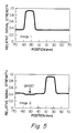
- Fig. 5 shows two such linescans where after erasure of Image 1 using light alone as shown in Fig. 3, a new Image 2 is taken where the ghost effect observed is a reversed image of a preceding image on the actual image display. The ghost appears at the moment the actual image is taken so there is no possibility to get rid of it by a substraction operation of the reference frame. It is obvious that such ghosts are not acceptable in a medical diagnostic perspective.
- the linescans constitute a plot of a relative signal strength versus position of the target-object.
- the relative signal strength can be related, as is known, to the voltage, the electric charge, the grey scale and the like.
- Fig. 6 illustrates one embodiment of the method of the present invention where the ghost is eliminated by uniformizing and decreasing the number of charges at the interface 22.
- point (A) of this figure there is shown the distribution of charges right after image formation by absorbtion of x-rays 15. Only the area where the target 17 was has an unchanged sensitivity, namely no negative charges at the interface 22.
- a high positive voltage is turned on and then the erasing light 21 is turned on. This produces the charge distribution shown at point (B) wherein the number of charges at the interface 22 is uniform within the plate 12.
- point (C) of Fig. 6 there is shown a charge distribution after the high voltage has been turned off while the light 21 is still applied to reduce the number of charges in the device. Then the light 21 is also turned off. There are still some negative charges remaining at the interface 22, which will reduce the sensitivity.
- Fig. 7 shows the result obtained from the method used according to Fig. 6. It shows the plot of relative signal strength as a function of position for the first and second images taken, where Image 2 was taken after erasure of Image 1 by the method described above in conjunction with Fig 6. Fig. 7 shows that unlike the result shown in Fig. 5, in this case there is no ghost visible.
- FIG. 8 Another embodiment of the erasure method of the present invention is illustrated in Fig. 8.
- the distribution of the charges at point (A) is identical to the one shown in Fig. 6, i.e. it shows such distribution right after the image frame and only the area where the target was has an unchanged sensitivity without any negative charges at the interface 22.
- This device is erased by turning on a high positive voltage by set-up 20 and then turning on the light 21, thereby uniformizing the interface 22 as shown at point (B).
- the high voltage is switched from positive to negative polarity during the erasure operation for just long enough to neutralize the negative charges at the interface 22. This is followed by turning the high voltage off and then turning the light off.
- the resulting charge distribution is shown a point (C) of Fig. 8. This results in very few negative charges being left at the interface 22 which is a highly desirable effect.
- Fig. 9 an alternative to the embodiment of Fig. 8 is illustrated.
- the operations at points (A) and (B) are identical to those shown in Fig. 8.
- the negative polarity voltage is maintained for a longer period of time than in Fig. 8 which produces accumulation of positive charges at interface 22. This, if left as such, would cause a large dark current to flow on the next reference frame which would not be satisfactory.
- the device is subjected to a high positive voltage bias without application of light as shown at point (D) of Fig. 9, before the next reference frame. This produces again a very satisfactory erasure of the x-ray device.
- the arrangement of Fig. 9 does not require as close a timing control for negative voltage bias as is required pursuant to Fig. 8.
- timing of high voltage and light it can be readily determined for various situations, such as the thickness of the photoreceptor, the luminance of light, etc.
- a person skilled in the art will determine and optimize such timing for any particular operation. However, to give an example of appropriate timings the following is suggested.
- Fig. 10 graphically illustrates the result obtained with the embodiments described in conjunction with Fig. 8 and Fig. 9, namely it shows no ghost in Image 2 and a sensitivity or relative signal strength similar to that of Image 1.
- the invention is not limited to embodiments described above by way of illustration, but that it includes any erasure method using a combination of high voltage and light.
- the two key steps used within the novel method are: (1) the uniformization of the interface, which occurs when the high voltage is on and the light is on at the same time, and (2) the neutralization of charges accumulated at the interface, which is achieved by reversing the high voltage polarity while leaving the light on; this second step is optional and is required only when decrease in sensitivity is objectionable.
- any erasure method comprising one or both of the above steps falls within the scope of the present invention.
Landscapes
- Health & Medical Sciences (AREA)
- Pathology (AREA)
- Physics & Mathematics (AREA)
- General Physics & Mathematics (AREA)
- Measurement Of Radiation (AREA)
- Transforming Light Signals Into Electric Signals (AREA)
- Apparatus For Radiation Diagnosis (AREA)
- Conversion Of X-Rays Into Visible Images (AREA)
Applications Claiming Priority (2)
| Application Number | Priority Date | Filing Date | Title |
|---|---|---|---|
| CA2200532 | 1997-03-20 | ||
| CA002200532A CA2200532C (en) | 1997-03-20 | 1997-03-20 | X-ray image erasure method |
Publications (3)
| Publication Number | Publication Date |
|---|---|
| EP0866378A2 true EP0866378A2 (de) | 1998-09-23 |
| EP0866378A3 EP0866378A3 (de) | 1999-12-08 |
| EP0866378B1 EP0866378B1 (de) | 2004-05-19 |
Family
ID=4160208
Family Applications (1)
| Application Number | Title | Priority Date | Filing Date |
|---|---|---|---|
| EP98301570A Expired - Lifetime EP0866378B1 (de) | 1997-03-20 | 1998-03-03 | Röntgenbildlöschvorrichtung |
Country Status (4)
| Country | Link |
|---|---|
| US (1) | US6078053A (de) |
| EP (1) | EP0866378B1 (de) |
| CA (1) | CA2200532C (de) |
| DE (1) | DE69823907T2 (de) |
Cited By (2)
| Publication number | Priority date | Publication date | Assignee | Title |
|---|---|---|---|---|
| EP1631067A3 (de) * | 2004-08-31 | 2008-09-03 | Xerox Corporation | Abbildungssystem und Verfahren, das eine elektrische Ladung aus einem Sensor entfernt |
| US9541667B2 (en) | 2013-09-04 | 2017-01-10 | United Parcel Service Of America, Inc. | X-ray scanning system and method |
Families Citing this family (9)
| Publication number | Priority date | Publication date | Assignee | Title |
|---|---|---|---|---|
| CA2363663C (en) * | 2001-11-22 | 2004-10-19 | Ftni Inc. | Direct conversion flat panel x-ray detector with automatic cancellation of ghost images |
| US9289024B2 (en) | 2007-04-16 | 2016-03-22 | Riddell, Inc. | Protective sports helmet |
| CN103119929B (zh) | 2010-09-13 | 2016-08-03 | 雷湾地区研究所 | 重置光导x射线成像检测器的系统和方法 |
| USD838922S1 (en) | 2011-05-02 | 2019-01-22 | Riddell, Inc. | Football helmet |
| KR20150027636A (ko) * | 2013-09-04 | 2015-03-12 | 삼성전자주식회사 | 잔류 전하 제거 방법, 이 방법을 이용한 엑스선 영상 촬영 방법 및 장치 |
| JP5952247B2 (ja) * | 2013-10-04 | 2016-07-13 | 富士フイルム株式会社 | 放射線画像撮影装置、消去光源の制御方法およびプログラム |
| JP6179362B2 (ja) * | 2013-11-14 | 2017-08-16 | コニカミノルタ株式会社 | ブライトバーンの消去方法およびブライトバーン消去機能を有する放射線画像撮影装置 |
| TWI535289B (zh) * | 2013-11-22 | 2016-05-21 | 財團法人工業技術研究院 | X光平板感測器之殘留電荷消除方法及裝置 |
| KR20160048538A (ko) | 2014-10-24 | 2016-05-04 | 삼성전자주식회사 | 엑스레이를 검출하는 장치 및 방법, 엑스레이 이미징 시스템 |
Family Cites Families (10)
| Publication number | Priority date | Publication date | Assignee | Title |
|---|---|---|---|---|
| US5414496A (en) * | 1989-09-21 | 1995-05-09 | Dai Nippon Printing Co., Ltd. | Method for manufacturing a printing plate using a charge carrier medium and method for page make-up using a charge carrier medium |
| DE69217940T2 (de) * | 1992-09-07 | 1997-09-11 | Agfa Gevaert Nv | Verfahren zum Auslöschen der gespeicherten Energie bei einem photostimulierbaren Phosphormittel |
| US5319206A (en) * | 1992-12-16 | 1994-06-07 | E. I. Du Pont De Nemours And Company | Method and apparatus for acquiring an X-ray image using a solid state device |
| US5661309A (en) * | 1992-12-23 | 1997-08-26 | Sterling Diagnostic Imaging, Inc. | Electronic cassette for recording X-ray images |
| US5563421A (en) * | 1995-06-07 | 1996-10-08 | Sterling Diagnostic Imaging, Inc. | Apparatus and method for eliminating residual charges in an image capture panel |
| EP0748115A1 (de) * | 1995-06-08 | 1996-12-11 | Agfa-Gevaert N.V. | Verfahren für die Aufnahme und die Wiedergabe eines Musters von eindringender elektromagnetischer Strahlung |
| US5925890A (en) * | 1995-06-08 | 1999-07-20 | Agfa-Gevaert N.V. | Apparatus for recording and reading out a pattern of penetrating electromagnetic radiation |
| US5665976A (en) * | 1995-09-05 | 1997-09-09 | Fuji Photo Film Co., Ltd. | Radiation image read-out and erasing method and apparatus |
| US5920070A (en) * | 1996-11-27 | 1999-07-06 | General Electric Company | Solid state area x-ray detector with adjustable bias |
| US5969360A (en) * | 1997-11-26 | 1999-10-19 | Direct Radiography Corp. | Readout sequence for residual image elimination in a radiation detection panel |
-
1997
- 1997-03-20 CA CA002200532A patent/CA2200532C/en not_active Expired - Lifetime
-
1998
- 1998-03-03 EP EP98301570A patent/EP0866378B1/de not_active Expired - Lifetime
- 1998-03-03 DE DE69823907T patent/DE69823907T2/de not_active Expired - Lifetime
- 1998-03-12 US US09/041,014 patent/US6078053A/en not_active Expired - Lifetime
Cited By (7)
| Publication number | Priority date | Publication date | Assignee | Title |
|---|---|---|---|---|
| EP1631067A3 (de) * | 2004-08-31 | 2008-09-03 | Xerox Corporation | Abbildungssystem und Verfahren, das eine elektrische Ladung aus einem Sensor entfernt |
| US9541667B2 (en) | 2013-09-04 | 2017-01-10 | United Parcel Service Of America, Inc. | X-ray scanning system and method |
| US9804289B2 (en) | 2013-09-04 | 2017-10-31 | United Parcel Service Of America, Inc. | X-ray scanning system and method |
| US10012755B2 (en) | 2013-09-04 | 2018-07-03 | United Parcel Service Of America, Inc. | X-ray scanning system and method |
| US10203426B2 (en) | 2013-09-04 | 2019-02-12 | United Parcel Service Of America, Inc. | X-ray scanning system and method |
| US10571597B2 (en) | 2013-09-04 | 2020-02-25 | United Parcel Service Of America, Inc. | X-ray scanning system and method |
| US11656188B2 (en) | 2013-09-04 | 2023-05-23 | United Parcel Service Of America, Inc. | X-ray scanning system and method |
Also Published As
| Publication number | Publication date |
|---|---|
| DE69823907T2 (de) | 2005-08-18 |
| CA2200532A1 (en) | 1998-09-20 |
| US6078053A (en) | 2000-06-20 |
| EP0866378A3 (de) | 1999-12-08 |
| EP0866378B1 (de) | 2004-05-19 |
| DE69823907D1 (de) | 2004-06-24 |
| CA2200532C (en) | 2002-02-26 |
Similar Documents
| Publication | Publication Date | Title |
|---|---|---|
| EP0747970B1 (de) | Vorrichtung für die Ableitung einer Restladung in einem Bildaufnahmesystem | |
| JP3404483B2 (ja) | ソリッド・ステート・デバイスを用いたx線イメージ捕獲エレメントおよび方法 | |
| EP0866378B1 (de) | Röntgenbildlöschvorrichtung | |
| EP0437041B1 (de) | Festkörperstrahlungsdetektor | |
| JP2835334B2 (ja) | X線像形成要素および該要素上に放射線像を形成する方法 | |
| US6376857B1 (en) | Read-out apparatus for an image detector | |
| Rowlands et al. | X‐ray imaging using amorphous selenium: A photoinduced discharge readout method for digital mammography | |
| US5168160A (en) | Method and apparatus for acquiring an electrical signal representing a radiographic image | |
| JPH06342099A (ja) | X線像記録用電子カセットおよびx線ラジオグラム撮影方法 | |
| JP3833712B2 (ja) | 捕捉電荷が減少する放射線イメージング用フラットパネル検出器 | |
| US3752572A (en) | Apparatus for making electrographs | |
| EP0028260A1 (de) | Gerät zur Abbildung von Objekten | |
| EP1114468B1 (de) | Direkter bildsensor für röntgenstrahlung mit einer dielektrischen schicht, die eine angepasste zeitkonstante aufweist | |
| CA1104190A (en) | Photocontrolled ion-flow electron radiography | |
| EP0823075B1 (de) | Verringerung von restpotential und geisterbildformung in einem photoleiter | |
| US4242433A (en) | High speed electrophotographic medium | |
| EP0574689A2 (de) | Verfahren und Vorrichtung zur Erfassung der Röntgenstrahlungsbild mittels einer Dünnschichttransistoren-Matrix | |
| US4433038A (en) | Electrophotographic copying process involving simultaneous charging and imaging | |
| US4392737A (en) | Electrophotographic copying apparatus | |
| US4442191A (en) | Electrophotographic copying process for producing a plurality of copies | |
| US4440844A (en) | Electrophotographic copying process involving simultaneous charging and imaging | |
| WO2002061456A2 (en) | Photoconductive imaging panel with externally controlled conductivity | |
| US4129779A (en) | Photocontrolled ion-flow electron radiography apparatus with multi-layered mesh structure | |
| JPH11218858A (ja) | X線撮像パネルの残留電荷除去方法 | |
| US4121101A (en) | Method of recording radiographic images |
Legal Events
| Date | Code | Title | Description |
|---|---|---|---|
| PUAI | Public reference made under article 153(3) epc to a published international application that has entered the european phase |
Free format text: ORIGINAL CODE: 0009012 |
|
| AK | Designated contracting states |
Kind code of ref document: A2 Designated state(s): BE CH DE DK FR GB IT LI NL SE |
|
| AX | Request for extension of the european patent |
Free format text: AL;LT;LV;MK;RO;SI |
|
| PUAL | Search report despatched |
Free format text: ORIGINAL CODE: 0009013 |
|
| AK | Designated contracting states |
Kind code of ref document: A3 Designated state(s): AT BE CH DE DK ES FI FR GB GR IE IT LI LU MC NL PT SE |
|
| AX | Request for extension of the european patent |
Free format text: AL;LT;LV;MK;RO;SI |
|
| RIC1 | Information provided on ipc code assigned before grant |
Free format text: 6G 03G 13/054 A, 6G 03G 15/054 B |
|
| 17P | Request for examination filed |
Effective date: 20000602 |
|
| AKX | Designation fees paid |
Free format text: BE CH DE DK FR GB IT LI NL SE |
|
| RAP1 | Party data changed (applicant data changed or rights of an application transferred) |
Owner name: ANRAD CORPORATION |
|
| 17Q | First examination report despatched |
Effective date: 20020521 |
|
| GRAP | Despatch of communication of intention to grant a patent |
Free format text: ORIGINAL CODE: EPIDOSNIGR1 |
|
| GRAS | Grant fee paid |
Free format text: ORIGINAL CODE: EPIDOSNIGR3 |
|
| GRAA | (expected) grant |
Free format text: ORIGINAL CODE: 0009210 |
|
| AK | Designated contracting states |
Kind code of ref document: B1 Designated state(s): BE CH DE DK FR GB IT LI NL SE |
|
| PG25 | Lapsed in a contracting state [announced via postgrant information from national office to epo] |
Ref country code: LI Free format text: LAPSE BECAUSE OF FAILURE TO SUBMIT A TRANSLATION OF THE DESCRIPTION OR TO PAY THE FEE WITHIN THE PRESCRIBED TIME-LIMIT Effective date: 20040519 Ref country code: IT Free format text: LAPSE BECAUSE OF FAILURE TO SUBMIT A TRANSLATION OF THE DESCRIPTION OR TO PAY THE FEE WITHIN THE PRESCRIBED TIME-LIMIT;WARNING: LAPSES OF ITALIAN PATENTS WITH EFFECTIVE DATE BEFORE 2007 MAY HAVE OCCURRED AT ANY TIME BEFORE 2007. THE CORRECT EFFECTIVE DATE MAY BE DIFFERENT FROM THE ONE RECORDED. Effective date: 20040519 Ref country code: CH Free format text: LAPSE BECAUSE OF FAILURE TO SUBMIT A TRANSLATION OF THE DESCRIPTION OR TO PAY THE FEE WITHIN THE PRESCRIBED TIME-LIMIT Effective date: 20040519 Ref country code: BE Free format text: LAPSE BECAUSE OF FAILURE TO SUBMIT A TRANSLATION OF THE DESCRIPTION OR TO PAY THE FEE WITHIN THE PRESCRIBED TIME-LIMIT Effective date: 20040519 |
|
| REG | Reference to a national code |
Ref country code: GB Ref legal event code: FG4D |
|
| REG | Reference to a national code |
Ref country code: CH Ref legal event code: EP |
|
| REF | Corresponds to: |
Ref document number: 69823907 Country of ref document: DE Date of ref document: 20040624 Kind code of ref document: P |
|
| PG25 | Lapsed in a contracting state [announced via postgrant information from national office to epo] |
Ref country code: SE Free format text: LAPSE BECAUSE OF FAILURE TO SUBMIT A TRANSLATION OF THE DESCRIPTION OR TO PAY THE FEE WITHIN THE PRESCRIBED TIME-LIMIT Effective date: 20040819 Ref country code: DK Free format text: LAPSE BECAUSE OF FAILURE TO SUBMIT A TRANSLATION OF THE DESCRIPTION OR TO PAY THE FEE WITHIN THE PRESCRIBED TIME-LIMIT Effective date: 20040819 |
|
| REG | Reference to a national code |
Ref country code: CH Ref legal event code: PL |
|
| ET | Fr: translation filed | ||
| PLBE | No opposition filed within time limit |
Free format text: ORIGINAL CODE: 0009261 |
|
| STAA | Information on the status of an ep patent application or granted ep patent |
Free format text: STATUS: NO OPPOSITION FILED WITHIN TIME LIMIT |
|
| 26N | No opposition filed |
Effective date: 20050222 |
|
| REG | Reference to a national code |
Ref country code: NL Ref legal event code: TD Effective date: 20130620 |
|
| REG | Reference to a national code |
Ref country code: FR Ref legal event code: CD Owner name: ANALOGIC CANADA CORPORATION Effective date: 20130618 |
|
| REG | Reference to a national code |
Ref country code: DE Ref legal event code: R082 Ref document number: 69823907 Country of ref document: DE Representative=s name: MUELLER-BORE & PARTNER PATENTANWAELTE PARTG MB, DE Effective date: 20130606 Ref country code: DE Ref legal event code: R082 Ref document number: 69823907 Country of ref document: DE Representative=s name: MUELLER-BORE & PARTNER PATENTANWAELTE, EUROPEA, DE Effective date: 20130606 Ref country code: DE Ref legal event code: R081 Ref document number: 69823907 Country of ref document: DE Owner name: ANALOGIC CANADA CORPORATION, SAINT-LAURENT, CA Free format text: FORMER OWNER: ANRAD CORP., SAINT-LAURENT, QUEBEC, CA Effective date: 20130606 Ref country code: DE Ref legal event code: R081 Ref document number: 69823907 Country of ref document: DE Owner name: ANALOGIC CANADA CORPORATION, CA Free format text: FORMER OWNER: ANRAD CORP., SAINT-LAURENT, CA Effective date: 20130606 |
|
| REG | Reference to a national code |
Ref country code: FR Ref legal event code: PLFP Year of fee payment: 19 |
|
| REG | Reference to a national code |
Ref country code: FR Ref legal event code: PLFP Year of fee payment: 20 |
|
| PGFP | Annual fee paid to national office [announced via postgrant information from national office to epo] |
Ref country code: NL Payment date: 20170321 Year of fee payment: 20 Ref country code: FR Payment date: 20170322 Year of fee payment: 20 Ref country code: DE Payment date: 20170322 Year of fee payment: 20 |
|
| PGFP | Annual fee paid to national office [announced via postgrant information from national office to epo] |
Ref country code: GB Payment date: 20170322 Year of fee payment: 20 |
|
| REG | Reference to a national code |
Ref country code: DE Ref legal event code: R071 Ref document number: 69823907 Country of ref document: DE |
|
| REG | Reference to a national code |
Ref country code: NL Ref legal event code: MK Effective date: 20180302 |
|
| REG | Reference to a national code |
Ref country code: GB Ref legal event code: PE20 Expiry date: 20180302 |
|
| PG25 | Lapsed in a contracting state [announced via postgrant information from national office to epo] |
Ref country code: GB Free format text: LAPSE BECAUSE OF EXPIRATION OF PROTECTION Effective date: 20180302 |