EP0884930A1 - Organic electroluminescent element and method for manufacturing the same - Google Patents
Organic electroluminescent element and method for manufacturing the same Download PDFInfo
- Publication number
- EP0884930A1 EP0884930A1 EP97904615A EP97904615A EP0884930A1 EP 0884930 A1 EP0884930 A1 EP 0884930A1 EP 97904615 A EP97904615 A EP 97904615A EP 97904615 A EP97904615 A EP 97904615A EP 0884930 A1 EP0884930 A1 EP 0884930A1
- Authority
- EP
- European Patent Office
- Prior art keywords
- inter
- insulator layer
- light
- layer
- organic
- Prior art date
- Legal status (The legal status is an assumption and is not a legal conclusion. Google has not performed a legal analysis and makes no representation as to the accuracy of the status listed.)
- Granted
Links
Images




Classifications
-
- H—ELECTRICITY
- H05—ELECTRIC TECHNIQUES NOT OTHERWISE PROVIDED FOR
- H05B—ELECTRIC HEATING; ELECTRIC LIGHT SOURCES NOT OTHERWISE PROVIDED FOR; CIRCUIT ARRANGEMENTS FOR ELECTRIC LIGHT SOURCES, IN GENERAL
- H05B33/00—Electroluminescent light sources
- H05B33/12—Light sources with substantially two-dimensional [2D] radiating surfaces
- H05B33/22—Light sources with substantially two-dimensional [2D] radiating surfaces characterised by the chemical or physical composition or the arrangement of auxiliary dielectric or reflective layers
-
- H—ELECTRICITY
- H05—ELECTRIC TECHNIQUES NOT OTHERWISE PROVIDED FOR
- H05B—ELECTRIC HEATING; ELECTRIC LIGHT SOURCES NOT OTHERWISE PROVIDED FOR; CIRCUIT ARRANGEMENTS FOR ELECTRIC LIGHT SOURCES, IN GENERAL
- H05B33/00—Electroluminescent light sources
- H05B33/02—Details
- H05B33/04—Sealing arrangements, e.g. against humidity
-
- H—ELECTRICITY
- H05—ELECTRIC TECHNIQUES NOT OTHERWISE PROVIDED FOR
- H05B—ELECTRIC HEATING; ELECTRIC LIGHT SOURCES NOT OTHERWISE PROVIDED FOR; CIRCUIT ARRANGEMENTS FOR ELECTRIC LIGHT SOURCES, IN GENERAL
- H05B33/00—Electroluminescent light sources
- H05B33/10—Apparatus or processes specially adapted to the manufacture of electroluminescent light sources
-
- H—ELECTRICITY
- H05—ELECTRIC TECHNIQUES NOT OTHERWISE PROVIDED FOR
- H05B—ELECTRIC HEATING; ELECTRIC LIGHT SOURCES NOT OTHERWISE PROVIDED FOR; CIRCUIT ARRANGEMENTS FOR ELECTRIC LIGHT SOURCES, IN GENERAL
- H05B33/00—Electroluminescent light sources
- H05B33/12—Light sources with substantially two-dimensional [2D] radiating surfaces
-
- H—ELECTRICITY
- H10—SEMICONDUCTOR DEVICES; ELECTRIC SOLID-STATE DEVICES NOT OTHERWISE PROVIDED FOR
- H10K—ORGANIC ELECTRIC SOLID-STATE DEVICES
- H10K50/00—Organic light-emitting devices
- H10K50/80—Constructional details
- H10K50/84—Passivation; Containers; Encapsulations
- H10K50/842—Containers
- H10K50/8426—Peripheral sealing arrangements, e.g. adhesives, sealants
-
- H—ELECTRICITY
- H10—SEMICONDUCTOR DEVICES; ELECTRIC SOLID-STATE DEVICES NOT OTHERWISE PROVIDED FOR
- H10K—ORGANIC ELECTRIC SOLID-STATE DEVICES
- H10K50/00—Organic light-emitting devices
- H10K50/80—Constructional details
- H10K50/84—Passivation; Containers; Encapsulations
- H10K50/842—Containers
- H10K50/8428—Vertical spacers, e.g. arranged between the sealing arrangement and the OLED
-
- H—ELECTRICITY
- H10—SEMICONDUCTOR DEVICES; ELECTRIC SOLID-STATE DEVICES NOT OTHERWISE PROVIDED FOR
- H10K—ORGANIC ELECTRIC SOLID-STATE DEVICES
- H10K50/00—Organic light-emitting devices
- H10K50/80—Constructional details
- H10K50/84—Passivation; Containers; Encapsulations
- H10K50/846—Passivation; Containers; Encapsulations comprising getter material or desiccants
-
- H—ELECTRICITY
- H10—SEMICONDUCTOR DEVICES; ELECTRIC SOLID-STATE DEVICES NOT OTHERWISE PROVIDED FOR
- H10K—ORGANIC ELECTRIC SOLID-STATE DEVICES
- H10K59/00—Integrated devices, or assemblies of multiple devices, comprising at least one organic light-emitting element covered by group H10K50/00
- H10K59/10—OLED displays
- H10K59/12—Active-matrix OLED [AMOLED] displays
- H10K59/122—Pixel-defining structures or layers, e.g. banks
-
- H—ELECTRICITY
- H10—SEMICONDUCTOR DEVICES; ELECTRIC SOLID-STATE DEVICES NOT OTHERWISE PROVIDED FOR
- H10K—ORGANIC ELECTRIC SOLID-STATE DEVICES
- H10K59/00—Integrated devices, or assemblies of multiple devices, comprising at least one organic light-emitting element covered by group H10K50/00
- H10K59/10—OLED displays
- H10K59/17—Passive-matrix OLED displays
- H10K59/173—Passive-matrix OLED displays comprising banks or shadow masks
-
- H—ELECTRICITY
- H10—SEMICONDUCTOR DEVICES; ELECTRIC SOLID-STATE DEVICES NOT OTHERWISE PROVIDED FOR
- H10K—ORGANIC ELECTRIC SOLID-STATE DEVICES
- H10K59/00—Integrated devices, or assemblies of multiple devices, comprising at least one organic light-emitting element covered by group H10K50/00
- H10K59/80—Constructional details
- H10K59/87—Passivation; Containers; Encapsulations
- H10K59/871—Self-supporting sealing arrangements
- H10K59/8722—Peripheral sealing arrangements, e.g. adhesives, sealants
-
- H—ELECTRICITY
- H10—SEMICONDUCTOR DEVICES; ELECTRIC SOLID-STATE DEVICES NOT OTHERWISE PROVIDED FOR
- H10K—ORGANIC ELECTRIC SOLID-STATE DEVICES
- H10K59/00—Integrated devices, or assemblies of multiple devices, comprising at least one organic light-emitting element covered by group H10K50/00
- H10K59/80—Constructional details
- H10K59/87—Passivation; Containers; Encapsulations
- H10K59/871—Self-supporting sealing arrangements
- H10K59/8723—Vertical spacers, e.g. arranged between the sealing arrangement and the OLED
-
- H—ELECTRICITY
- H10—SEMICONDUCTOR DEVICES; ELECTRIC SOLID-STATE DEVICES NOT OTHERWISE PROVIDED FOR
- H10K—ORGANIC ELECTRIC SOLID-STATE DEVICES
- H10K59/00—Integrated devices, or assemblies of multiple devices, comprising at least one organic light-emitting element covered by group H10K50/00
- H10K59/80—Constructional details
- H10K59/87—Passivation; Containers; Encapsulations
- H10K59/874—Passivation; Containers; Encapsulations including getter material or desiccant
-
- H—ELECTRICITY
- H10—SEMICONDUCTOR DEVICES; ELECTRIC SOLID-STATE DEVICES NOT OTHERWISE PROVIDED FOR
- H10K—ORGANIC ELECTRIC SOLID-STATE DEVICES
- H10K71/00—Manufacture or treatment specially adapted for the organic devices covered by this subclass
- H10K71/10—Deposition of organic active material
- H10K71/16—Deposition of organic active material using physical vapour deposition [PVD], e.g. vacuum deposition or sputtering
-
- H—ELECTRICITY
- H10—SEMICONDUCTOR DEVICES; ELECTRIC SOLID-STATE DEVICES NOT OTHERWISE PROVIDED FOR
- H10K—ORGANIC ELECTRIC SOLID-STATE DEVICES
- H10K59/00—Integrated devices, or assemblies of multiple devices, comprising at least one organic light-emitting element covered by group H10K50/00
-
- H—ELECTRICITY
- H10—SEMICONDUCTOR DEVICES; ELECTRIC SOLID-STATE DEVICES NOT OTHERWISE PROVIDED FOR
- H10K—ORGANIC ELECTRIC SOLID-STATE DEVICES
- H10K59/00—Integrated devices, or assemblies of multiple devices, comprising at least one organic light-emitting element covered by group H10K50/00
- H10K59/80—Constructional details
- H10K59/805—Electrodes
Definitions
- the present invention relates to an organic electroluminescent element. More particularly, the present invention is concerned with an organic electroluminescent element( hereinafter sometimes abbreviated to" organic EL element ”) which, when used for a display and the like, is highly precise and minute, uniformly emits light, and can withstand external pressure.
- organic electroluminescent element hereinafter sometimes abbreviated to" organic EL element
- Japanese Patent Application Laid-Open No.250583/1991 discloses an organic EL element which is equipped with an interlaminar insulating film, and thus has favorable pattern precision as well as high uniformity in a light-emitting surface.
- a masking vapor deposition method is applied to the production of a counter electrode, it has been still difficult to produce a highly precise and minute display having a line pitch of 300 ⁇ m or less.
- Japanese Patent Application Laid-Open No.101884/1993 discloses an organic EL element which is equipped with an inter-insulator layer, and the outside surface of which is covered with a moisture-resistant film. Nevertheless the organic EL element thus disclosed has still involved the problem that because of the insufficient sealing power of the moisture-resistant film, a cathode is attacked by moisture or oxygen after being allowed to stand for several thousands hours, thus bringing about a dark spot, that is, defective light emission.
- Japanese Patent Application Laid-Open No. 275172/1993 discloses a highly precise and minute display having a line pitch of about 100 ⁇ m, by equipping an organic EL element with an inter-insulator layer in the form of wall, and also forming a cathode by means of oblique vapor deposition.
- the display disclosed above has still involved the problem that minute short circuit is caused by reason of the deviation of the alloy composition in the edges( the end away from the inter-insulator layer ) of the electrode that is formed through vapor deposition in an oblique direction to the substrate.
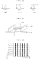
- the first aspect of the present invention provides an organic elecrtoluminescent element 1 that is equipped, between a lower electrode 3 and a counter eletrode 4 each on a substrate 2, with an intervening organic layer 5 comprising a light-emitting layer, which element 1 comprises an inter-insulator layer 6 having a coefficient of water absorption of at most 0.1% in a non-light-emitting element portion; step portions 9 in said inter-insulator layer 6 which define the boundary between a light-emitting element portion and a non-light-emitting element portion and which contain rising parts almost perpendicular to the surface of said lower electrode 3; and a sealing plate or a sealing lid 7 which is placed over said inter-insulator layer 6 and which is attached to said substrate 2 via an adhesive layer 8.
- element 1 comprises an inter-insulator layer 6 having a coefficient of water absorption of at most 0.1% in a non-light-emitting element portion
- step portions 9 in said inter-insulator layer 6 which define the boundary between a light-emitting
- the second aspect of the present invention provides a process for producing an organic elecrtoluminescent element 1, comprising at least one step of forming a lower electrode 3 on a substrate 2; a step of forming a patterned inter -insulator layer 6 on said lower electrode 3; a step of forming an organic layer 5 on said lower electrode 3; and at least one step of forming a counter electrode 4 in the form of film, so that step portions 9 in said inter-insulator layer 6 define the boundary between a light-emitting element portion and a non-light-emitting element portion and also contain rising parts almost perpendicular to the surface of said lower electrode 3, said counter electrode 4 is cut off by said step portions 9 at the rising parts so as to be subjected to patterning processing, and said counter electrode 4 is in close contact with said inter-insulator layer 6 at said step portions 9 adjacent to said substrate 2.
- the third aspect of the present invention provides an organic elecrtoluminescent element 1 that is equipped, between a lower electrode 3 and a counter eletrode 4 each on a substrate 2, with an intervening organic layer 5 comprising a light-emitting layer, which element 1 comprises an interl-insulator layer 6 having a coefficient of water absorption of at most 0.1% in a non-light-emitting element portion; step portions 9 in said inter-insulator layer 6 which contain portions rising in the form of an inverse taper almost perpendicularly to the surface of the lower electrode 3 and divide said counter electrode 4 into a plurality of individuals; and a sealing plate or a sealing lid 7 which is placed over said inter-insulator layer 6 and which is attached to said substrate 2 via an adhesive layer 8.
- the fourth aspect of the present invention provides an organic elecrtoluminescent element 1 that is equipped, between a lower electrode 3 and a counter eletrode 4 each on a substrate 2, with an intervening organic layer 5 comprising a light-emitting layer, which element 1 comprises a first inter-insulator layer having a trapezoidal cross section 15 on said lower elecrode 3 as a non-light-emitting element portion; a second inter-insulator layer 14 above said trapezoidal cross section ( on the opposite side of said lower electrode 3 ) ; step portions 9 in said second inter -insulator layer 14 which contain rising parts almost perpendicular to the surface of the lower electrode 3 and divide said counter electrode 4 into a plurality of individuals ; and a sealing plate or a sealing lid 7 which is placed over said second inter-insulator layer 14 and which is attached to said substrate 2 via an adhesive layer 8.( Refer to FIG.2. )
- inter-insulator layer which constitutes the organic electroluminescent element according to the present invention.
- a constitution of an organic electroluminescent element in which an organic layer allowing current to flow is made to intervene between a pair of a lower electrode and a counter electrode.
- a portion in which an insulator layer is made to intervene between a lower electrode and a counter electrode prevents current from flowing, and accordingly can not emit light.
- Such an insulator layer is designated as inter-insulator layer.
- a technique is known, which carries out pattern processing of a light emitting element by the pattern processing of an inter-insulator layer [ refer to Japanese Patent Application Laid-Open No.250583/1991( Hei-3 )].
- a ⁇ ( h / 7 ) is preferable, and a ⁇ ( h / 10 ) is particularly preferable. It is made to a ⁇ 0 when the step portions are processed to form an inversely tapered shape, which is one of the most preferable configurations in the present invention.
- the height of an inter-insulator layer( h ) is preferably in the range of 0.5 m ⁇ to 50 m ⁇ . The height of an inter-insulator layer ( h ), when being in the aforestated range, enables a counter electrode 4 to be cut off at the step portions of the interinsulator layer and at the same time, to be subjected to patterning processing.
- the step portions 9 of the inter-insulator layer rise almost perpendicular, it is made possible thereby to spontaneously cut off the counter electrode at the step portion 9, and thus to pattern process the counter electrode by dispensing with a special method such as the oblique vapor deposition.
- the counter electrode 4 of the light-emitting element portion is in contact with the cross section of the adjacent inter-insulator layer 6 at the pattern processed portion.
- the first and second aspects of the present invention are each characterized by the absence of a counter electrode 4 which is apart from said cross section, whereby the advantages of the present invention are derived( FIG.5 ). In the following, the working effects due to the above advantages will be described.
- the third aspect of the present invention it is possible to cut off the counter electrode 4 at the step portion 9 and to process patterning of the same.
- the deposits are prevented from adhering to the step portion, thereby enabling more reliable cutting off.
- the advantages in the third aspect of the present invention are same as the description in the items (a) and (b), thereby enabling high resolution and high density patterning of the cathode.
- the counter electrode 4 must not entirely cover the organic layer 5, or cause short circuits to the lower electrode 3.
- the second inter-insulator layer 14 may be inversely tapered, or may be such that satisfying the inequality a ⁇ ( h/10 ).
- An inter-insulator layer of low hygroscopicity is preferably used in addition to that of insulating property.
- Particularly preferable inter-insulator layer 6 is that having a water absorption( coefficient of water absorption) of at most 0.1% .
- An inter-insulator layer of high hygroscopicity causes, in the case of preserving the elements, oozing out of water which has mixed in during the preparation, thereby oxidizes the electrode of the element, deteriorates the element and further becomes responsible for defects in light emitting elements ( dark spot ).
- the use of a polymer of low hygroscopicity is preferable because of its excellent processability in particular.
- Particularly preferable inter-insulator layer is that of fluorine base or polyolefin base. The hygroscopicity is evaluated as coefficient of water absorption according to ASTM D-570.
- the inter-insulator layer is not necessarily required to hold a photosensitive function, but preferably holds such a function in some cases, since said function enables photolithography without the use of a photoresist.
- a photosensitive material is available from the market whether it is an inorganic oxide or a polymer.
- a solution of a polymer or a precursor thereof is made into a film by means of coating, spin coating, dipping or the like process ( refer to FIG.7 ).
- a variety of film preparation processes are available including vapor deposition, CVD, plasma CVD, ECR-CVD, sputtering, ECR-sputtering and the like processes.
- the patterning of a photoresist is carried out by photosensitizing any of various available photoresists, and developing the same ( refer to FIG.8 ).
- a photoresist and an exposure method are each selected in accordance with the minuteness and precision of the pattern that are required in each case.
- Various exposure methods are known and exemplified by contact exposure method and cutback exposure method.
- a portion uncovered with a photoresist is removed by any of various etching methods ( refer to FIG. 9 ).
- the etching methods include wet etching method in which an inter-insulator layer is dissolved and removed with a solvent and dry etching method in which an inter-insulator layer is decomposed and removed with a plasma or the like. In order to allow an inter-insulator to rise almost perpendicular to the surface of the lower electrode 3, the dry etching method is preferable.
- a suitable etching gas dry etching by the use of oxygen plasma is preferable for such a polymer as fluorinated polyimides, polyolefins and polyquinolines.
- fluorine-based polymers fluorine-added SiO 2 , SiO 3 and Al 2 O 3
- a fluorinated carbonized gas include CHF 3 and CF 4 .
- a counter electrode 4, when being used as a cathode, is preferably made of an alloy containing an alkali metal or an alloy containing an alkaline earth metal.
- particularly preferable alloys among them include Mg : Ag, Al : Li, Pb : Li, Zn : Li, Bi : Li, Ln : Li, Al : Ca, etc. It is known that the above-exemplified alloys are relatively corrosion-resistant and have each a low work function.
- a vapor deposition method and a sputtering method are preferably used.
- a vapor deposition method and a sputtering method are preferably used.
- the vapor deposition should be carried out perpendicularly to the surface of a substrate.
- a counter electrode 4, when being used as an anode, is preferably made of a transparent oxide.
- particularly preferable oxide include ITO, ZnO : Al, SnO 2 : Sb and InZnO( indium / zinc oxide ).
- a sealing plate is positioned over the inter -insulator layer 6 or the second inter-insulator layer 14.
- Preferable materials of construction for the sealing plate or sealing lid are glass, an oxide and a nitride ceramic each in the form of a thin plate.
- Preferable thickness of the sealing plate or sealing lid is 5 ⁇ m to 2 mm, and it is at most 500 ⁇ m in order to obtain particularly thin organic EL element.
- the inter-insulator layer 6 or the second inter-insulator layer 14 functions as a column, and prevents the sealing plate from coming into contact with the body of the organic EL element. It is therefore, made possible to thin the organic EL element in whole by thinning the sealing plate 7, without causing any problem even if the sealing plate 7 is thinned as thin as 50 ⁇ m.
- the preferred embodiments of the sealing plate are as follows.
- step portions of the inter-insulator layer in the present invention it is possible to form portions where the counter electrode 4 is not cut off.
- the counter electrode 4 is not cut off.
- a taper of a > ( h / 5 ) is processed,at the step portion 9, there is no need for cutting the counter electrode.
- a portion that is encompassed by a rising cross-section and a taper cross-section can be formed at the opening of the inter-insulator layer which constitute the light emitting element portion by a method wherein two layers of the inter-insulator layers are formed, specifically, by allowing a first step portion of the film to rise perpendicularly and subjecting a second step portion of the film to taper processing.
- the counter electrode is cut off at the rising portion, but is not cut off at the taper cross-section.
- the fourth and the fifth aspects of the present invention take advantage of the foregoing facts. That is to say, at the first inter-insulator layer 15, the cross section is formed into a trapezoidal shape so that the counter electrode may not be cut off and so that the film is used for establishing the light-emitting pixel surface. On the contrary, at the second inter-insulator layer 14, the step portions are made to rise almost perpendicularly so that the counter electrode may be cut off and so as to enable patterning by taking advantage of the layer.
- a counter electrode 4 may not be formed on the inter-insulator layer [ refer to Japanese Patent Application Laid-Open No.250583 /1991( Hei-3 )]. Accordingly, a portion free from a counter electrode 4 can be formed on the inter-insulator layer.
- the circuit as illustrated in FIG.14 is incorporated per each pixel in active matrix driving using a transistor.
- opening portions of the inter-insulator layer according to the present invention are provided only at the end portion 25 and the portion corresponding to the pixel electrode, it follows that the counter electrodes Tr 1 and Tr 2 , the counter electrodes on SCAN( 20 ), DATA( 21 ), and COMMON( 22 ) and the counter electrode on the pixel electrode are insulated by the step portions of the inter -insulator layer.
- an additional inter-insulator layer is installed in advance on the portion at which the SCAN, DATA, and COMMON intersect the counter electrode 4, on the portion at which the COMMON intersects the SCAN, and also on the portion at which the SCAN intersects the DATA so as to insulate one another.
- the above-mentioned additional inter -insulator layer different from the inter-insulator layer according to the present invention, are not equipped with perpendicular step portions so that the electrode wires above the additional inter-insulator layer may not be cut off. Accordingly, it is acceptable in the present invention to partially use an inter-insulator layer having non-perpendicular step portions.
- the film-coated substrate was baked in a hot oven at 70°C for 30 mimutes, and then was exposed to light through a photomask at an irradiation power of 120 mJ /cm 2 with ultraviolet ray at a wavelength of 436 nm.
- the exposure pattern was carried out so that the ZCOAT-1410 as the inter-insulator layer having a width of 20 ⁇ m remained at every 100 ⁇ m as linear lines perpendicularly to the pattern of the aforesasid ITO pattern.
- curing was put into practice at 250°C for 2 hours in a clean oven to prepare an inter-insulator layer.
- the specimen that had been prepared in the preceding Example 1 was broken at an arbitrary point thereof into ten specimens sized 2 mm ⁇ 2 mm, the cross sections of which were observed by the use of a scanning electron microscopy. Thus, measurements were performed to obtain the value: ⁇ ( width of the lower section) - ( width of the upper section) ⁇ / ( height ) at 20 places of the specimens . As a result, the value was 1/ 10 or less for all of the specimens.
- measurements were performed to obtain the coefficient of water absorption ( moisture absorption ) of the specimen which had been prepared in Example 1. As a result, the the moisture absorption showed favorable values of 0.07% ( in accordance with ASTM D 570 ).
- Example 1 The specimen which had been prepared in Example 1 was cleaned with ultrasonic wave in isopropyl alcohol for 3 minutes, and further with a cleaning apparatus using the combination of ultraviolet ray and ozone for 30 minutes. Subsequently, the specimen was placed in a vacuum deposition apparatus available from the market( produced by ULVAC JAPAN Ltd.), and was fixed to a substrate holder.
- TPD N,N'-diphenyl-N,N'-bis-(3-methylphenyl)-[1,1'-biphenyl ]-4, 4'-diamine
- the TPD-containig boat was heated to form a hole transporting layer having a film thickness of 80 nm.
- a light-emitting layer in the form of film consist- ing of Alq and having a film thickness of 75 nm on the hole transporting layer.
- Mg and a tungsten basket containing silver that were placed in a resistacne heating boat and prepared in advance in a vaccum chamber were heated to prepare a film of Mg-Ag counter electrode having a film thickness of 200 nm at vapor deposition rates of Mg and Ag of 1.4 nm /sec. and 0.1 nm /sec., respectivly.
- the sealing plate used herein was a glass plate with a thickness of 100 ⁇ m which had been subjected to dehydration treatment by the use of a dehydrating agent which had been prepared by dispersing silica-gel in a solution of soluble nylon.
- a dehydrating agent which had been prepared by dispersing silica-gel in a solution of soluble nylon.
- the periphery of the sealing plate was coated with a ultraviolet ray curing adhesive, and the sealing plate and the organic EL element were attached to each other to seal them by ultraviolet ray irradiation.
- a sealed organic EL element according to the present invention was completed.
- the resultant sealed organic EL element had a thickness as small as 0.6 mm, thus demonstrating the efffectiveness of the organic EL element according to the present invention as described hereinbefore.
- the non-light-emission state for the edges of the stripe lines was examined at the same time. As the result, it has been proved that the non-light-emission width thereof was 3 ⁇ m or smaller, and also that the edges were favorably defined.
- the sealing plate was pressed with fingers to check any short-circuits of the element. As the result, the element was entirely free from any short-circuits, since the inter-insulator layer was in the form of a column.
- a photosensitive polyimide coating material (produced by Toray Industries Inc. under the trade name "UR 3140” ) was applied by spin coating onto a glass substrate holding an ITO as the lower electrode which had been subjected to striped processing, said glass substrate being the same as that used in Example 1.
- the spin coating was carried out at a number of revolutions of 4000rpm for a revolution time of 30 seconds. Subsequently, the coated substrate was dried at 80°C for 30 mimutes, and then was exposed to light through a photomask at an irradiation power of 80 mJ /cm 2 .
- a pattern of the polymer of a polyamic acid was obtained.
- the resultant pattern was cured at 180°C for 30 minutes in an oven in an N 2 atmosphere , and further cured at 300°C for 30 minutes, thus enabling to prepare an ITO/glass substrate with a polyimide layer as an inter-insulator layer.
- the resultant ITO/glass substrate was tesed in the same manner as in Example 2.
- the value: ⁇ ( width of the lower section) - ( width of the upper section) ⁇ / ( height ) was about 1 .
- an organic EL element was prepared, and one line of ITO and one line of Mg : Ag were selected out of the stripe lines.
- Example 4 [ In the case of the inter-insulator layer being a fluorine-based polymer ]
- a solution of a fluorine-based resin( produced by Asahi Glass Co.,Ltd. under the trade name " Sitop CTX-809 ") capable of forming an inter-insulator layer made of a fluorine-based resin having a coefficient of water absorption of at most 0.01% was applied by spin coating onto a glass substrate same as that used in Example 1.
- the spin coating was carried out at a number of revolutions of 600 rpm for a revolution time of 30 seconds to form a Sitop film with a film thickness of 4.8 ⁇ m.
- the coated substrate was dried on a hot plate at 50°C for 1 mimute, at 80°C for 1 mimute, and at 120°C for 1 mimute. As the final curing it was further dried in an oven at 250°C for 1 hour.
- etching was carried out for 50 minutes by means of a plasma etcher as a dry etching apparatus, using a mixed gas containing CF 4 , CHF 3 , and Ar at flow rates of 24, 24, and 98 SCCm, respectively at a plasma output of 300 W under a vacuum degree of 0.5 Torr.
- ZCOAT-1410 photosensitive polyolefin-based nagative type resist, produced by Nippon Zeon Co.,Ltd.
- ZCOAT-1410 photosensitive polyolefin-based nagative type resist, produced by Nippon Zeon Co.,Ltd.
- the spin coating was carried out at a number of revolutions of 1000rpm for a revolution time of 40 seconds.
- the film thus obtained had a thickness of 8.8 ⁇ m.
- the film-coated substrate was baked in a hot oven at 80°C for 15 mimutes, and then was exposed to light through a photomask at an irradiation power of 450 mJ / cm 2 with ultraviolet ray with a wavelength of 365 nm.
- the exposure pattern was carried out so that an inter-insulator layer having a width of 50 ⁇ m remains at a pitch of 350 ⁇ m as linear lines perpendicularly to the pattern of the aforesasid ITO pattern.
- curing was put into practice at 200°C for 1 hour in a clean oven to prepare an inter-insulator layer.
- Example 5 By the use of the specimen which had been prepared in Example 5, an organic EL element was prepared in the same manner as in Example 3. The pattern precision was evaluated in the same manner as in Example 3. As the result, the pattern precision was ⁇ 4 ⁇ m, and it was confirmed that the pattern was free from any short-circuited connection part in the stripe lines of Mg : Ag, thereby demonstrating the favorable patterning method.
- SiO 2 was made into a film with a thickness of 1 ⁇ m by a plasma-enhanced CVD method on a glass substrate 2 with a thickness of 0.5 mm holding an ITO as the lower electrode which had been subjected to striped processing at a pitch of 300 ⁇ m.
- the film formation conditions were set to a substrate temperature of 250°C , a vacuum degree of 0.7 Torr, and a plasma output of 200 W, using a mixed gas of N 2 O and SiH 4 ( 1:1 ) as the plasma gas species.
- a positive type photoresist produced by Tokyo Ohka Kogyo Co., Ltd. under the trade name" TOPR-1000 .
- the opening lines had a width of 280 ⁇ m and a pitch of 300 ⁇ m.
- the SiO 2 at the opening portion of the photoresist was completely removed by plasma etching so that the surface of the ITO was exposed.
- the SiO 2 etching was carried out, using a mixed gas of CF 4 , CHF 3 , and Ar ( ratio by volume of 1 : 1 : 3.5 ) as the plasma gas species at a vacuum degree of 0.5 Torr, and a plasma output of 300 W.
- the SiO 2 that was used as the inter-insulator layer had an extremely low coefficient of water absorption as low as 0.01 % or lower.
- a positive type photoresist produced by Tokyo Ohka Kogyo Co.,Ltd. under the trade name" TOPR-1000 .
- the opening lines had a width of 280 ⁇ m and a pitch of 350 ⁇ m.
- the photoresist along with the substrate was heated to 150°C so that the cross section of the photoresist was made into a semicylindrical shape.
- etching was carried out with a plasma etcher under the etching conditions including a mixed gas of CF 4 , CHF 3 , and Ar ( ratio by volume of 1 : 1 : 8 ) as the plasma gas species, a vacuum degree of 0.2 Torr, and a plasma output of 200 W.
- a plasma etcher under the etching conditions including a mixed gas of CF 4 , CHF 3 , and Ar ( ratio by volume of 1 : 1 : 8 ) as the plasma gas species, a vacuum degree of 0.2 Torr, and a plasma output of 200 W.
Landscapes
- Engineering & Computer Science (AREA)
- Manufacturing & Machinery (AREA)
- Physics & Mathematics (AREA)
- Optics & Photonics (AREA)
- Microelectronics & Electronic Packaging (AREA)
- Electroluminescent Light Sources (AREA)
Abstract
Description
Claims (5)
- An organic elecrtoluminescent element 1 that is equipped, between a lower electrode 3 and a counter eletrode 4 each on a substrate 2, with an intervening organic layer 5 comprising a light-emitting layer, which element 1 comprises an inter-insulator layer 6 having a coefficient of water absorption of at most 0.1% in a non-light-emitting element portion; step portions 9 in said inter-insulator layer 6 which define the boundary between a light-emitting element portion and a non-light-emitting element portion and which contain rising parts almost perpendicular to the surface of said lower electrode 3; and a sealing plate or a sealing lid 7 which is placed over said inter-insulator layer 6 and which is attached to said substrate 2 via an adhesive layer 8.
- A process for producing an organic elecrtoluminescent element 1, comprising at least one step of forming a lower electrode 3 on a substrate 2; a step of forming a patterned inter-insulator layer 6 on said lower electrode 3; a step of forming an organic layer 5 over said lower electrode 3; and at least one step of forming a counter electrode 4 in the form of film, so that step portions 9 in said inter-insulator layer 6 define the boundary between a light-emitting element portion and a non-light-emitting element portion, and also comprises rising parts almost perpendicular to the surface of said lower electrode 3, said counter electrode 4 is cut off by said step portions 9 at said rising parts so as to be subjected to patterning processing, and said counter electrode 4 is in close contact with said inter-insulator layer 6 at said step portions 9 adjacent to said substrate 2.
- An organic elecrtoluminescent element 1 that is equipped, between a lower electrode 3 and a counter eletrode 4 each on a substrate 2, with an intervening organic layer 5 comprising a light-emitting layer, which element 1 comprises an inter-insulator layer 6 having a coefficient of water absorption of at most 0.1% in a non-light-emitting element portion; step portions 9 in said inter-insulator layer 6 which contain portions rising in the form of an inverse taper almost perpendicularly to the surface of the lower electrode 3 and divide said counter electrode 4 into a plurality of individuals; and, a sealing plate or a sealing lid 7 which is placed over said inter-insulator layer 6 and which is attached to said substrate 2 via an adhesive layer 8.
- An organic elecrtoluminescent element 1 that is equipped, between a lower electrode 3 and a counter eletrode 4 each on a substrate 2, with an intervening organic layer 5 comprising a light-emitting layer, which element 1 comprises a first inter-insulator layer having a trapezoidal cross section 15 on said lower elecrode 3 as a non-light-emitting element portion; a second inter-insulator layer 14 above said trapezoidal cross section; step portions 9 in said second inter-insulator layer 14 which contain rising parts almost perpendicular to the surface of the lower electrode 3 and divide said counter electrode 4 into a plurality of individuals ; and a sealing plate or a sealing lid 7 which is placed over said second inter-insulator layer 14 and which is attached to said substrate 2 via an adhesive layer 8.
- A process for producing an organic elecrtoluminescent element 1, comprising at least one step of forming a lower electrode 3 on a substrate 2 ; a step of forming a patterned inter-insulator layer on said lower electrode 3, a step of forming an organic layer over said lower electrode 3 , and at least one step of forming a counter electrode 4 in the form of film, so that a first inter-insulator layer 15 has a trapezoidal cross section, a second inter-insulator layer 14 is mounted above said trapezoidal cross section, step portions 9 in said second inter-insulator layer 14 contain rising parts almost perpendicular to the surface of said lower electrode 3, and said counter electrode 4 is subjected to patterning processing at said rising part.
Priority Applications (1)
| Application Number | Priority Date | Filing Date | Title |
|---|---|---|---|
| EP07101139A EP1773103B1 (en) | 1996-02-26 | 1997-02-24 | Organic electroluminescent element and method for manufacturing same |
Applications Claiming Priority (5)
| Application Number | Priority Date | Filing Date | Title |
|---|---|---|---|
| JP38217/96 | 1996-02-26 | ||
| JP3821796 | 1996-02-26 | ||
| JP30167896 | 1996-11-13 | ||
| JP301678/96 | 1996-11-13 | ||
| PCT/JP1997/000508 WO1997031508A1 (en) | 1996-02-26 | 1997-02-24 | Organic electroluminescent element and method for manufacturing the same |
Related Child Applications (2)
| Application Number | Title | Priority Date | Filing Date |
|---|---|---|---|
| EP07101139A Division EP1773103B1 (en) | 1996-02-26 | 1997-02-24 | Organic electroluminescent element and method for manufacturing same |
| EP07101139.9 Division-Into | 2007-01-25 |
Publications (3)
| Publication Number | Publication Date |
|---|---|
| EP0884930A1 true EP0884930A1 (en) | 1998-12-16 |
| EP0884930A4 EP0884930A4 (en) | 1999-04-28 |
| EP0884930B1 EP0884930B1 (en) | 2010-09-29 |
Family
ID=26377414
Family Applications (2)
| Application Number | Title | Priority Date | Filing Date |
|---|---|---|---|
| EP97904615A Expired - Lifetime EP0884930B1 (en) | 1996-02-26 | 1997-02-24 | Organic electroluminescent element and method for manufacturing the same |
| EP07101139A Expired - Lifetime EP1773103B1 (en) | 1996-02-26 | 1997-02-24 | Organic electroluminescent element and method for manufacturing same |
Family Applications After (1)
| Application Number | Title | Priority Date | Filing Date |
|---|---|---|---|
| EP07101139A Expired - Lifetime EP1773103B1 (en) | 1996-02-26 | 1997-02-24 | Organic electroluminescent element and method for manufacturing same |
Country Status (7)
| Country | Link |
|---|---|
| US (2) | US6175186B1 (en) |
| EP (2) | EP0884930B1 (en) |
| JP (1) | JP3247388B2 (en) |
| KR (1) | KR100500078B1 (en) |
| DE (2) | DE69739955D1 (en) |
| TW (1) | TW334513B (en) |
| WO (1) | WO1997031508A1 (en) |
Cited By (25)
| Publication number | Priority date | Publication date | Assignee | Title |
|---|---|---|---|---|
| EP0892588A3 (en) * | 1997-07-18 | 1999-09-15 | TDK Corporation | Organic electroluminescent display |
| EP0938248A3 (en) * | 1998-02-18 | 1999-09-29 | Eastman Kodak Company | Organic electroluminescent image display panel with multiple barriers |
| WO2000019776A1 (en) * | 1998-09-30 | 2000-04-06 | Koninklijke Philips Electronics N.V. | Method and device for manufacturing an electroluminescent display screen |
| WO2000069002A1 (en) * | 1999-05-11 | 2000-11-16 | The Dow Chemical Company | An electroluminescent or photocell device having protective packaging |
| WO2001019142A1 (en) * | 1999-09-03 | 2001-03-15 | Uniax Corporation | Encapsulation of organic electronic devices |
| WO2002005361A1 (en) * | 2000-07-12 | 2002-01-17 | 3M Innovative Properties Company | Encapsulated organic electronic devices and method for making same |
| WO2003044875A1 (en) * | 2001-11-20 | 2003-05-30 | Osram Opto Semiconductors Gmbh | Improved patterning of electrodes in oled devices with shaped pillars |
| GB2383192A (en) * | 2001-09-05 | 2003-06-18 | Light Display Corp G | Encapsulation structure, method and apparatus for organic light-emitting diodes |
| WO2003098973A1 (en) * | 2002-05-15 | 2003-11-27 | Koninklijke Philips Electronics N.V. | Method of manufacturing a flat panel display |
| EP1076369A3 (en) * | 1999-08-12 | 2004-06-09 | Eastman Kodak Company | A method of making an organic electroluminescent device |
| EP0917410B1 (en) * | 1997-09-18 | 2004-08-18 | Lg Electronics Inc. | Method for fabricating an organic electroluminescent device |
| EP1526589A2 (en) | 2003-10-21 | 2005-04-27 | Lg Electronics Inc. | Electro luminescence display device |
| EP1253643A3 (en) * | 2001-04-23 | 2006-05-17 | Sel Semiconductor Energy Laboratory Co., Ltd. | Display device and method of manufacturing the same |
| US7247878B2 (en) | 2002-12-28 | 2007-07-24 | Lg.Philips Lcd Co., Ltd. | Dual panel-type organic electroluminescent device |
| EP1834347A1 (en) * | 2004-12-27 | 2007-09-19 | Osram Opto Semiconductors GmbH | Electroluminescent organic light emitting device and production method thereof |
| US7326653B2 (en) | 2002-03-27 | 2008-02-05 | Cambridge Display Technology Limited | Method of preparation of organic optoelectronic and electronic devices and devices thereby obtained |
| US7408191B2 (en) | 2001-05-22 | 2008-08-05 | Semiconductor Energy Laboratory Co., Ltd. | Luminescent device and process of manufacturing the same |
| US7438829B2 (en) | 2003-11-13 | 2008-10-21 | E.I. Du Pont De Nemours And Company | Thick film getter paste compositions for use in moisture control |
| US7501671B2 (en) | 2001-01-19 | 2009-03-10 | Semiconductor Energy Laboratory Co., Ltd. | Semiconductor device and method of manufacturing the same |
| US7633223B2 (en) * | 2000-11-10 | 2009-12-15 | Semiconductor Energy Laboratory Co., Ltd. | Organic light emitting device provided with drying agent at side surfaces of a sealing member |
| US7691288B2 (en) | 2005-07-18 | 2010-04-06 | E.I. Du Pont De Nemours And Company | Thick film getter paste compositions with pre-hydrated desiccant for use in atmosphere control |
| DE10357472B4 (en) * | 2002-12-13 | 2010-05-12 | Lg Display Co., Ltd. | Organic double panel electroluminescent display and method of making the same |
| US7952103B2 (en) | 1999-09-17 | 2011-05-31 | Semiconductor Energy Laboratory Co., Ltd. | EL display device and method for manufacturing the same |
| US8110983B2 (en) | 1999-10-29 | 2012-02-07 | Semiconductor Energy Laboratory Co., Ltd. | Self light emitting device |
| US8957584B2 (en) | 1999-10-29 | 2015-02-17 | Semiconductor Energy Laboratory Co., Ltd. | Self light-emitting device |
Families Citing this family (56)
| Publication number | Priority date | Publication date | Assignee | Title |
|---|---|---|---|---|
| KR100500078B1 (en) * | 1996-02-26 | 2005-07-18 | 이데미쓰 고산 가부시키가이샤 | Organic electroluminescent element and method for manufacturing the same |
| JP3520396B2 (en) * | 1997-07-02 | 2004-04-19 | セイコーエプソン株式会社 | Active matrix substrate and display device |
| JP3580092B2 (en) * | 1997-08-21 | 2004-10-20 | セイコーエプソン株式会社 | Active matrix display |
| EP1505648A3 (en) * | 1997-08-21 | 2005-08-10 | Seiko Epson Corporation | Active matrix display device |
| JP3428397B2 (en) * | 1997-10-14 | 2003-07-22 | 松下電器産業株式会社 | Organic electroluminescent device and method of manufacturing the same |
| GB2335884A (en) * | 1998-04-02 | 1999-10-06 | Cambridge Display Tech Ltd | Flexible substrates for electronic or optoelectronic devices |
| JPH11339968A (en) * | 1998-05-25 | 1999-12-10 | Sanyo Electric Co Ltd | Organic electroluminescence device |
| KR100635429B1 (en) * | 1998-08-03 | 2006-10-18 | 듀폰 디스플레이즈, 인크. | Encapsulation of Polymer-Based Solid Devices Using Inorganic Materials |
| JP3807114B2 (en) * | 1998-08-25 | 2006-08-09 | カシオ計算機株式会社 | Method for manufacturing light emitting device |
| CN1227731C (en) * | 1999-07-09 | 2005-11-16 | 材料研究及工程研究所 | Laminates for encapsulating components |
| ATE376707T1 (en) | 1999-07-09 | 2007-11-15 | Osram Opto Semiconductors Gmbh | ENCAPSULATION OF A DEVICE |
| JP4942867B2 (en) * | 1999-09-17 | 2012-05-30 | 株式会社半導体エネルギー研究所 | EL display device and electronic device |
| US6833668B1 (en) * | 1999-09-29 | 2004-12-21 | Sanyo Electric Co., Ltd. | Electroluminescence display device having a desiccant |
| US6876145B1 (en) * | 1999-09-30 | 2005-04-05 | Semiconductor Energy Laboratory Co., Ltd. | Organic electroluminescent display device |
| KR100381054B1 (en) * | 1999-12-28 | 2003-04-18 | 엘지.필립스 엘시디 주식회사 | Transparent Electrode Composed of Indium-Zinc-Oxide and Etchant For Etching The Same |
| US6633121B2 (en) * | 2000-01-31 | 2003-10-14 | Idemitsu Kosan Co., Ltd. | Organic electroluminescence display device and method of manufacturing same |
| JP3755727B2 (en) * | 2000-02-21 | 2006-03-15 | 富士電機ホールディングス株式会社 | Organic thin film light emitting display panel and method for manufacturing the same |
| JP2002182380A (en) * | 2000-12-14 | 2002-06-26 | Jsr Corp | Radiation-sensitive resin composition for forming insulating film of organic EL display element, insulating film formed therefrom, and organic EL display element |
| JP3915402B2 (en) * | 2000-12-05 | 2007-05-16 | Jsr株式会社 | Radiation sensitive resin composition for forming insulating film of organic EL display element, insulating film formed therefrom, and organic EL display element |
| JP3909552B2 (en) * | 2000-07-27 | 2007-04-25 | Jsr株式会社 | Radiation-sensitive resin composition and insulating film for organic EL device |
| JP2002056986A (en) * | 2000-08-09 | 2002-02-22 | Korai Kagi Kofun Yugenkoshi | Organic electroluminescent device having heat radiation effect and method of manufacturing the same |
| JP2002151252A (en) * | 2000-11-16 | 2002-05-24 | Stanley Electric Co Ltd | Organic EL display |
| JP4665333B2 (en) * | 2000-11-27 | 2011-04-06 | 東レ株式会社 | Positive photosensitive resin precursor composition |
| US6724150B2 (en) | 2001-02-01 | 2004-04-20 | Semiconductor Energy Laboratory Co., Ltd. | Display device and manufacturing method thereof |
| US6984546B2 (en) * | 2001-03-15 | 2006-01-10 | Delta Optoelectronics, Inc. | Method for forming a thin film light emitting device |
| JP2002289347A (en) * | 2001-03-27 | 2002-10-04 | Sanyo Electric Co Ltd | ELECTROLUMINESCENT DISPLAY, ITS MANUFACTURING METHOD, DEPOSITION MASK, AND ITS MANUFACTURING METHOD |
| JP4511072B2 (en) * | 2001-03-30 | 2010-07-28 | 三洋電機株式会社 | Electroluminescent device with shock absorbing function and sealing member with shock absorbing function for electroluminescent device |
| JP4090786B2 (en) * | 2001-05-22 | 2008-05-28 | 株式会社半導体エネルギー研究所 | Light emitting device |
| US7005799B2 (en) * | 2001-07-30 | 2006-02-28 | Intel Corporation | Sealing organic light emitting device displays |
| US7158559B2 (en) * | 2002-01-15 | 2007-01-02 | Tensor Comm, Inc. | Serial cancellation receiver design for a coded signal processing engine |
| US7148624B2 (en) * | 2002-05-07 | 2006-12-12 | Osram Opto Semiconductors (Malaysia) Sdn. Bhd | Uniform deposition of organic layer |
| US7423375B2 (en) * | 2002-05-07 | 2008-09-09 | Osram Gmbh | Encapsulation for electroluminescent devices |
| KR20040009348A (en) * | 2002-07-23 | 2004-01-31 | 삼성 엔이씨 모바일 디스플레이 주식회사 | Dual-type organic electro luminesence display and the method for manufacturing the same |
| KR100675625B1 (en) * | 2002-08-08 | 2007-02-01 | 엘지.필립스 엘시디 주식회사 | Organic electroluminescent device and manufacturing method thereof |
| JP2005071646A (en) * | 2003-08-28 | 2005-03-17 | Chi Mei Electronics Corp | Organic EL display and manufacturing method thereof |
| KR100705312B1 (en) * | 2004-03-22 | 2007-04-10 | 엘지전자 주식회사 | Organic electroluminescent device and manufacturing method thereof |
| KR20070049172A (en) * | 2004-08-26 | 2007-05-10 | 이데미쓰 고산 가부시키가이샤 | Organic EL display |
| KR100603836B1 (en) * | 2004-11-30 | 2006-07-24 | 엘지.필립스 엘시디 주식회사 | Organic electroluminescent device and manufacturing method thereof |
| JP4655266B2 (en) * | 2005-02-08 | 2011-03-23 | セイコーエプソン株式会社 | Electro-optical device and electronic apparatus |
| JP2006228578A (en) * | 2005-02-17 | 2006-08-31 | Dainippon Printing Co Ltd | Color filter substrate for organic electroluminescent device |
| JP2007073332A (en) * | 2005-09-07 | 2007-03-22 | Konica Minolta Holdings Inc | Organic electroluminescence panel and method for producing organic electroluminescence panel |
| KR101157262B1 (en) * | 2005-12-14 | 2012-06-15 | 엘지디스플레이 주식회사 | Organic electro-luminescence display device and method for fabricating of the same |
| JP4663554B2 (en) * | 2006-03-09 | 2011-04-06 | 株式会社半導体エネルギー研究所 | Method for manufacturing display device |
| JP4663560B2 (en) * | 2006-03-17 | 2011-04-06 | 株式会社半導体エネルギー研究所 | Car audio, sound reproduction device and portable information terminal |
| US8022624B2 (en) * | 2007-04-25 | 2011-09-20 | Global Oled Technology Llc | Moisture protection for OLED display |
| JP4678421B2 (en) | 2008-05-16 | 2011-04-27 | ソニー株式会社 | Display device |
| JP4656204B2 (en) * | 2008-07-28 | 2011-03-23 | セイコーエプソン株式会社 | Display device |
| KR101073561B1 (en) | 2009-02-05 | 2011-10-17 | 삼성모바일디스플레이주식회사 | organic electro luminescence display and method for fabricating the same |
| JP5409830B2 (en) * | 2012-02-21 | 2014-02-05 | 株式会社半導体エネルギー研究所 | Light emitting device |
| TWI496328B (en) * | 2012-04-24 | 2015-08-11 | Innocom Tech Shenzhen Co Ltd | Organic light emitting diode display device and method of manufacturing same |
| CN103325949A (en) * | 2013-05-24 | 2013-09-25 | 四川虹视显示技术有限公司 | Organic light emitting diode packaging structure and preparation method thereof |
| JP5728531B2 (en) * | 2013-06-20 | 2015-06-03 | 株式会社半導体エネルギー研究所 | EL display device |
| JP6113633B2 (en) * | 2013-11-27 | 2017-04-12 | 株式会社ジャパンディスプレイ | Organic EL display device and manufacturing method thereof |
| CN108630829B (en) * | 2017-03-17 | 2019-11-08 | 京东方科技集团股份有限公司 | Manufacturing method of display panel, display panel and display device |
| EP3661327A1 (en) * | 2017-07-26 | 2020-06-03 | Light Flex Technology, S.L. | Laminar luminaire and method of manufacture |
| US10675657B2 (en) * | 2018-07-10 | 2020-06-09 | Visera Technologies Company Limited | Optical elements and method for fabricating the same |
Family Cites Families (14)
| Publication number | Priority date | Publication date | Assignee | Title |
|---|---|---|---|---|
| JP2734464B2 (en) | 1990-02-28 | 1998-03-30 | 出光興産株式会社 | Electroluminescence device and method of manufacturing the same |
| JPH03261091A (en) * | 1990-03-09 | 1991-11-20 | Pioneer Electron Corp | Electroluminescent element |
| JPH04242099A (en) * | 1991-01-16 | 1992-08-28 | Sharp Corp | Manufacture of thin film electroluminescence(el) panel |
| JP2813495B2 (en) * | 1991-07-26 | 1998-10-22 | 出光興産株式会社 | Organic EL element sealing method |
| JPH05101884A (en) * | 1991-10-11 | 1993-04-23 | Idemitsu Kosan Co Ltd | Sealing method and patterning method of organic electroluminescent element |
| US5276380A (en) * | 1991-12-30 | 1994-01-04 | Eastman Kodak Company | Organic electroluminescent image display device |
| JPH0565097U (en) * | 1992-02-07 | 1993-08-27 | 株式会社ケンウッド | Structure of thin film EL device |
| JP3813217B2 (en) * | 1995-03-13 | 2006-08-23 | パイオニア株式会社 | Method for manufacturing organic electroluminescence display panel |
| US5804917A (en) * | 1995-01-31 | 1998-09-08 | Futaba Denshi Kogyo K.K. | Organic electroluminescent display device and method for manufacturing same |
| JP3208638B2 (en) | 1995-01-31 | 2001-09-17 | 双葉電子工業株式会社 | Organic electroluminescent display device and method of manufacturing the same |
| JP3401356B2 (en) * | 1995-02-21 | 2003-04-28 | パイオニア株式会社 | Organic electroluminescent display panel and method of manufacturing the same |
| JP4142117B2 (en) | 1995-10-06 | 2008-08-27 | パイオニア株式会社 | Organic electroluminescence display panel and manufacturing method thereof |
| JPH09283280A (en) * | 1996-02-16 | 1997-10-31 | Mitsubishi Chem Corp | Method for manufacturing organic electroluminescent device |
| KR100500078B1 (en) * | 1996-02-26 | 2005-07-18 | 이데미쓰 고산 가부시키가이샤 | Organic electroluminescent element and method for manufacturing the same |
-
1997
- 1997-02-24 KR KR10-2004-7008847A patent/KR100500078B1/en not_active Expired - Lifetime
- 1997-02-24 EP EP97904615A patent/EP0884930B1/en not_active Expired - Lifetime
- 1997-02-24 JP JP52999497A patent/JP3247388B2/en not_active Expired - Lifetime
- 1997-02-24 EP EP07101139A patent/EP1773103B1/en not_active Expired - Lifetime
- 1997-02-24 US US09/117,286 patent/US6175186B1/en not_active Expired - Lifetime
- 1997-02-24 DE DE69739955T patent/DE69739955D1/en not_active Expired - Lifetime
- 1997-02-24 DE DE69740011T patent/DE69740011D1/en not_active Expired - Lifetime
- 1997-02-24 WO PCT/JP1997/000508 patent/WO1997031508A1/en not_active Ceased
- 1997-02-25 TW TW086102259A patent/TW334513B/en not_active IP Right Cessation
-
2000
- 2000-11-22 US US09/717,222 patent/US6498428B1/en not_active Expired - Lifetime
Cited By (57)
| Publication number | Priority date | Publication date | Assignee | Title |
|---|---|---|---|---|
| US6114805A (en) * | 1997-07-18 | 2000-09-05 | Tdk Corporation | Organic electroluminescent display with filter layer |
| EP0892588A3 (en) * | 1997-07-18 | 1999-09-15 | TDK Corporation | Organic electroluminescent display |
| EP0917410B1 (en) * | 1997-09-18 | 2004-08-18 | Lg Electronics Inc. | Method for fabricating an organic electroluminescent device |
| EP0938248A3 (en) * | 1998-02-18 | 1999-09-29 | Eastman Kodak Company | Organic electroluminescent image display panel with multiple barriers |
| WO2000019776A1 (en) * | 1998-09-30 | 2000-04-06 | Koninklijke Philips Electronics N.V. | Method and device for manufacturing an electroluminescent display screen |
| WO2000069002A1 (en) * | 1999-05-11 | 2000-11-16 | The Dow Chemical Company | An electroluminescent or photocell device having protective packaging |
| US6383664B2 (en) | 1999-05-11 | 2002-05-07 | The Dow Chemical Company | Electroluminescent or photocell device having protective packaging |
| EP1076369A3 (en) * | 1999-08-12 | 2004-06-09 | Eastman Kodak Company | A method of making an organic electroluminescent device |
| WO2001019142A1 (en) * | 1999-09-03 | 2001-03-15 | Uniax Corporation | Encapsulation of organic electronic devices |
| US8450745B2 (en) | 1999-09-17 | 2013-05-28 | Semiconductor Energy Laboratory Co., Ltd. | EL display device |
| US9735218B2 (en) | 1999-09-17 | 2017-08-15 | Semiconductor Energy Laboratory Co., Ltd. | EL display device and method for manufacturing the same |
| US8735900B2 (en) | 1999-09-17 | 2014-05-27 | Semiconductor Energy Laboratory Co., Ltd. | EL display device |
| US8183571B2 (en) | 1999-09-17 | 2012-05-22 | Semiconductor Energy Laboratory Co., Ltd. | EL display device and method for manufacturing the same |
| US7952103B2 (en) | 1999-09-17 | 2011-05-31 | Semiconductor Energy Laboratory Co., Ltd. | EL display device and method for manufacturing the same |
| US9059049B2 (en) | 1999-09-17 | 2015-06-16 | Semiconductor Energy Laboratory Co., Ltd. | EL display device |
| US9431470B2 (en) | 1999-09-17 | 2016-08-30 | Semiconductor Energy Laboratory Co., Ltd. | Display device |
| US8110983B2 (en) | 1999-10-29 | 2012-02-07 | Semiconductor Energy Laboratory Co., Ltd. | Self light emitting device |
| US8957584B2 (en) | 1999-10-29 | 2015-02-17 | Semiconductor Energy Laboratory Co., Ltd. | Self light-emitting device |
| US9299955B2 (en) | 1999-10-29 | 2016-03-29 | Semiconductor Energy Laboratory Co., Ltd. | Self light-emitting device |
| US8657985B2 (en) | 2000-07-12 | 2014-02-25 | 3M Innovative Properties Company | Encapsulated organic electronic devices and method for making same |
| WO2002005361A1 (en) * | 2000-07-12 | 2002-01-17 | 3M Innovative Properties Company | Encapsulated organic electronic devices and method for making same |
| US6867539B1 (en) | 2000-07-12 | 2005-03-15 | 3M Innovative Properties Company | Encapsulated organic electronic devices and method for making same |
| US7049630B2 (en) | 2000-09-06 | 2006-05-23 | Osram Opto Semiconductors (Malaysia) Sdn. Bhd | Electrode patterning in OLED devices |
| US6930321B2 (en) | 2000-09-06 | 2005-08-16 | Osram Opto Semiconductors (Malaysia) Sdn. Bhd | Robust electrode patterning in OLED devices |
| US6699728B2 (en) | 2000-09-06 | 2004-03-02 | Osram Opto Semiconductors Gmbh | Patterning of electrodes in oled devices |
| US7633223B2 (en) * | 2000-11-10 | 2009-12-15 | Semiconductor Energy Laboratory Co., Ltd. | Organic light emitting device provided with drying agent at side surfaces of a sealing member |
| US7501671B2 (en) | 2001-01-19 | 2009-03-10 | Semiconductor Energy Laboratory Co., Ltd. | Semiconductor device and method of manufacturing the same |
| EP2259323A3 (en) * | 2001-04-23 | 2011-03-02 | Semiconductor Energy Laboratory Co, Ltd. | Display device and method of manufacturing the same |
| US7405515B2 (en) | 2001-04-23 | 2008-07-29 | Semiconductor Energy Laboratory Co., Ltd. | Display device and method of manufacturing the same |
| EP1253643A3 (en) * | 2001-04-23 | 2006-05-17 | Sel Semiconductor Energy Laboratory Co., Ltd. | Display device and method of manufacturing the same |
| US8853940B2 (en) | 2001-04-23 | 2014-10-07 | Semiconductor Energy Laboratory Co., Ltd. | Display device with seal member |
| US8415881B2 (en) | 2001-04-23 | 2013-04-09 | Semiconductor Energy Laboratory Co., Ltd. | Display device and method of manufacturing the same |
| US9368561B2 (en) | 2001-05-22 | 2016-06-14 | Semiconductor Enery Laboratory Co., Ltd. | Luminescent device having light-emitting element and transistor |
| US8450741B2 (en) | 2001-05-22 | 2013-05-28 | Semiconductor Energy Laboratory Co., Ltd. | Luminescent device and process of manufacturing the same |
| US9761645B2 (en) | 2001-05-22 | 2017-09-12 | Semiconductor Energy Laboratory Co., Ltd. | Luminescent device having light emitting element and transistor |
| US7408191B2 (en) | 2001-05-22 | 2008-08-05 | Semiconductor Energy Laboratory Co., Ltd. | Luminescent device and process of manufacturing the same |
| US8803152B2 (en) | 2001-05-22 | 2014-08-12 | Semiconductor Energy Laboratory Co., Ltd. | Luminescent device and process of manufacturing the same |
| US8022404B2 (en) | 2001-05-22 | 2011-09-20 | Semiconductor Energy Laboratory Co., Ltd. | Luminescent device and process of manufacturing the same |
| US10103211B2 (en) | 2001-05-22 | 2018-10-16 | Semiconductor Energy Laboratory Co., Ltd. | Luminescent device having light-emitting element and transistor |
| GB2383192A (en) * | 2001-09-05 | 2003-06-18 | Light Display Corp G | Encapsulation structure, method and apparatus for organic light-emitting diodes |
| GB2383192B (en) * | 2001-09-05 | 2003-12-17 | Light Display Corp G | Encapsulation structure, method, and apparatus for organic light-emitting diodes |
| WO2003044875A1 (en) * | 2001-11-20 | 2003-05-30 | Osram Opto Semiconductors Gmbh | Improved patterning of electrodes in oled devices with shaped pillars |
| US7326653B2 (en) | 2002-03-27 | 2008-02-05 | Cambridge Display Technology Limited | Method of preparation of organic optoelectronic and electronic devices and devices thereby obtained |
| WO2003098973A1 (en) * | 2002-05-15 | 2003-11-27 | Koninklijke Philips Electronics N.V. | Method of manufacturing a flat panel display |
| DE10357472B4 (en) * | 2002-12-13 | 2010-05-12 | Lg Display Co., Ltd. | Organic double panel electroluminescent display and method of making the same |
| US7247878B2 (en) | 2002-12-28 | 2007-07-24 | Lg.Philips Lcd Co., Ltd. | Dual panel-type organic electroluminescent device |
| DE10360870B4 (en) * | 2002-12-28 | 2010-11-11 | Lg Display Co., Ltd. | Active matrix OELD and process for its preparation |
| US7550306B2 (en) | 2002-12-28 | 2009-06-23 | Lg Display Co., Ltd. | Dual panel-type organic electroluminescent device and method for fabricating the same |
| US7189990B2 (en) | 2003-10-21 | 2007-03-13 | Lg Electronics Inc. | Electro luminescence display device |
| EP1526589A3 (en) * | 2003-10-21 | 2006-07-26 | Lg Electronics Inc. | Electro luminescence display device |
| EP1526589A2 (en) | 2003-10-21 | 2005-04-27 | Lg Electronics Inc. | Electro luminescence display device |
| US7943059B2 (en) | 2003-11-13 | 2011-05-17 | E. I. Du Pont De Nemours And Company | Thick film getter paste compositions for use in moisture control |
| US7699999B2 (en) | 2003-11-13 | 2010-04-20 | E.I. Du Pont De Nemours And Company | Thick film getter paste compositions for use in moisture control |
| US7438829B2 (en) | 2003-11-13 | 2008-10-21 | E.I. Du Pont De Nemours And Company | Thick film getter paste compositions for use in moisture control |
| EP1834347A1 (en) * | 2004-12-27 | 2007-09-19 | Osram Opto Semiconductors GmbH | Electroluminescent organic light emitting device and production method thereof |
| US7943060B2 (en) | 2005-07-18 | 2011-05-17 | E.I. Du Pont De Nemours And Company | Thick film getter paste compositions with pre-hydrated desiccant for use in atmosphere control |
| US7691288B2 (en) | 2005-07-18 | 2010-04-06 | E.I. Du Pont De Nemours And Company | Thick film getter paste compositions with pre-hydrated desiccant for use in atmosphere control |
Also Published As
| Publication number | Publication date |
|---|---|
| EP1773103A2 (en) | 2007-04-11 |
| EP1773103A3 (en) | 2008-04-02 |
| US6498428B1 (en) | 2002-12-24 |
| KR20040059492A (en) | 2004-07-05 |
| DE69739955D1 (en) | 2010-09-16 |
| JP3247388B2 (en) | 2002-01-15 |
| EP1773103B1 (en) | 2010-08-04 |
| KR100500078B1 (en) | 2005-07-18 |
| EP0884930B1 (en) | 2010-09-29 |
| EP0884930A4 (en) | 1999-04-28 |
| WO1997031508A1 (en) | 1997-08-28 |
| DE69740011D1 (en) | 2010-11-11 |
| TW334513B (en) | 1998-06-21 |
| US6175186B1 (en) | 2001-01-16 |
Similar Documents
| Publication | Publication Date | Title |
|---|---|---|
| EP1773103B1 (en) | Organic electroluminescent element and method for manufacturing same | |
| US6198220B1 (en) | Sealing structure for organic light emitting devices | |
| JPWO1997031508A1 (en) | Organic electroluminescent element and manufacturing method thereof | |
| US7863814B2 (en) | Organic electroluminescent device comprising a stack partition structure | |
| US6608283B2 (en) | Apparatus and method for solder-sealing an active matrix organic light emitting diode | |
| US6146715A (en) | Method of fabricating organic electroluminescent display panel | |
| US20010044035A1 (en) | Organic EL element and method of manufacturing the same | |
| JPH10223376A (en) | Organic electroluminescent display device and method of manufacturing the same | |
| JP2011513944A (en) | Water barrier sealing method | |
| CN1802877A (en) | Organic semiconductor device and its manufacturing method | |
| JPH1154285A (en) | Organic electroluminescence device | |
| CA2295676A1 (en) | Sealing structure for organic light emitting devices | |
| US6853130B2 (en) | Organic electroluminescent device and manufacturing method therefor | |
| JP2001326069A (en) | Organic electroluminescence device and method of manufacturing the same | |
| JPH10261486A (en) | Method for manufacturing organic EL light emitting device | |
| JPH10247587A (en) | Organic electroluminescent display device and method of manufacturing the same | |
| KR101347471B1 (en) | Organic el device and method of manufacturing organic el device | |
| JP3575468B2 (en) | Manufacturing method of organic EL display | |
| KR20070011105A (en) | Self-emission panel and method of manufacturing the same | |
| JP2004014236A (en) | Manufacturing method of organic EL element | |
| KR100453427B1 (en) | Organic electroluminescent element and method for manufacturing the same | |
| KR100417921B1 (en) | Canless Organic Electro Luminescence Display | |
| EP0995212A1 (en) | Anhydrous method of packaging organic light emitting displays | |
| JP2003297550A (en) | Light emitting element, display device using the same, and lighting device | |
| JP2008108590A (en) | Organic EL device and manufacturing method thereof |
Legal Events
| Date | Code | Title | Description |
|---|---|---|---|
| PUAI | Public reference made under article 153(3) epc to a published international application that has entered the european phase |
Free format text: ORIGINAL CODE: 0009012 |
|
| 17P | Request for examination filed |
Effective date: 19980811 |
|
| AK | Designated contracting states |
Kind code of ref document: A1 Designated state(s): BE CH DE FR GB IT LI NL SE |
|
| RIN1 | Information on inventor provided before grant (corrected) |
Inventor name: HOSOKAWA, CHISHIO-IDEMITSU KOSAN CO., LTD. Inventor name: EIDA, MITSURU-IDEMITSU KOSAN CO., LTD. Inventor name: MATSUURA, MASAHIDE |
|
| A4 | Supplementary search report drawn up and despatched |
Effective date: 19990317 |
|
| AK | Designated contracting states |
Kind code of ref document: A4 Designated state(s): BE CH DE FR GB IT LI NL SE |
|
| 17Q | First examination report despatched |
Effective date: 20040608 |
|
| 17Q | First examination report despatched |
Effective date: 20040608 |
|
| GRAP | Despatch of communication of intention to grant a patent |
Free format text: ORIGINAL CODE: EPIDOSNIGR1 |
|
| GRAS | Grant fee paid |
Free format text: ORIGINAL CODE: EPIDOSNIGR3 |
|
| GRAA | (expected) grant |
Free format text: ORIGINAL CODE: 0009210 |
|
| AK | Designated contracting states |
Kind code of ref document: B1 Designated state(s): BE CH DE FR GB IT LI NL SE |
|
| REG | Reference to a national code |
Ref country code: GB Ref legal event code: FG4D |
|
| REG | Reference to a national code |
Ref country code: CH Ref legal event code: EP |
|
| REF | Corresponds to: |
Ref document number: 69740011 Country of ref document: DE Date of ref document: 20101111 Kind code of ref document: P |
|
| REG | Reference to a national code |
Ref country code: NL Ref legal event code: VDEP Effective date: 20100929 |
|
| PG25 | Lapsed in a contracting state [announced via postgrant information from national office to epo] |
Ref country code: SE Free format text: LAPSE BECAUSE OF FAILURE TO SUBMIT A TRANSLATION OF THE DESCRIPTION OR TO PAY THE FEE WITHIN THE PRESCRIBED TIME-LIMIT Effective date: 20100929 |
|
| PG25 | Lapsed in a contracting state [announced via postgrant information from national office to epo] |
Ref country code: IT Free format text: LAPSE BECAUSE OF FAILURE TO SUBMIT A TRANSLATION OF THE DESCRIPTION OR TO PAY THE FEE WITHIN THE PRESCRIBED TIME-LIMIT Effective date: 20100929 Ref country code: NL Free format text: LAPSE BECAUSE OF FAILURE TO SUBMIT A TRANSLATION OF THE DESCRIPTION OR TO PAY THE FEE WITHIN THE PRESCRIBED TIME-LIMIT Effective date: 20100929 |
|
| PG25 | Lapsed in a contracting state [announced via postgrant information from national office to epo] |
Ref country code: BE Free format text: LAPSE BECAUSE OF FAILURE TO SUBMIT A TRANSLATION OF THE DESCRIPTION OR TO PAY THE FEE WITHIN THE PRESCRIBED TIME-LIMIT Effective date: 20100929 |
|
| PLBE | No opposition filed within time limit |
Free format text: ORIGINAL CODE: 0009261 |
|
| STAA | Information on the status of an ep patent application or granted ep patent |
Free format text: STATUS: NO OPPOSITION FILED WITHIN TIME LIMIT |
|
| 26N | No opposition filed |
Effective date: 20110630 |
|
| REG | Reference to a national code |
Ref country code: CH Ref legal event code: PL |
|
| REG | Reference to a national code |
Ref country code: DE Ref legal event code: R097 Ref document number: 69740011 Country of ref document: DE Effective date: 20110630 |
|
| PG25 | Lapsed in a contracting state [announced via postgrant information from national office to epo] |
Ref country code: CH Free format text: LAPSE BECAUSE OF NON-PAYMENT OF DUE FEES Effective date: 20110228 Ref country code: LI Free format text: LAPSE BECAUSE OF NON-PAYMENT OF DUE FEES Effective date: 20110228 |
|
| PGFP | Annual fee paid to national office [announced via postgrant information from national office to epo] |
Ref country code: FR Payment date: 20120227 Year of fee payment: 16 |
|
| PGFP | Annual fee paid to national office [announced via postgrant information from national office to epo] |
Ref country code: GB Payment date: 20120227 Year of fee payment: 16 |
|
| PGFP | Annual fee paid to national office [announced via postgrant information from national office to epo] |
Ref country code: DE Payment date: 20120414 Year of fee payment: 16 |
|
| GBPC | Gb: european patent ceased through non-payment of renewal fee |
Effective date: 20130224 |
|
| REG | Reference to a national code |
Ref country code: FR Ref legal event code: ST Effective date: 20131031 |
|
| REG | Reference to a national code |
Ref country code: DE Ref legal event code: R119 Ref document number: 69740011 Country of ref document: DE Effective date: 20130903 |
|
| PG25 | Lapsed in a contracting state [announced via postgrant information from national office to epo] |
Ref country code: FR Free format text: LAPSE BECAUSE OF NON-PAYMENT OF DUE FEES Effective date: 20130228 Ref country code: DE Free format text: LAPSE BECAUSE OF NON-PAYMENT OF DUE FEES Effective date: 20130903 Ref country code: GB Free format text: LAPSE BECAUSE OF NON-PAYMENT OF DUE FEES Effective date: 20130224 |