EP0887843B1 - Verfahren zur Herstellung eines Transistors mit einem Silizium-Germanium-Gatter - Google Patents
Verfahren zur Herstellung eines Transistors mit einem Silizium-Germanium-Gatter Download PDFInfo
- Publication number
- EP0887843B1 EP0887843B1 EP98401432A EP98401432A EP0887843B1 EP 0887843 B1 EP0887843 B1 EP 0887843B1 EP 98401432 A EP98401432 A EP 98401432A EP 98401432 A EP98401432 A EP 98401432A EP 0887843 B1 EP0887843 B1 EP 0887843B1
- Authority
- EP
- European Patent Office
- Prior art keywords
- layer
- deposition
- etching
- gate
- silicon
- Prior art date
- Legal status (The legal status is an assumption and is not a legal conclusion. Google has not performed a legal analysis and makes no representation as to the accuracy of the status listed.)
- Expired - Lifetime
Links
Images


Classifications
-
- H—ELECTRICITY
- H10—SEMICONDUCTOR DEVICES; ELECTRIC SOLID-STATE DEVICES NOT OTHERWISE PROVIDED FOR
- H10D—INORGANIC ELECTRIC SEMICONDUCTOR DEVICES
- H10D64/00—Electrodes of devices having potential barriers
- H10D64/01—Manufacture or treatment
- H10D64/013—Manufacture or treatment of electrodes having a conductor capacitively coupled to a semiconductor by an insulator
- H10D64/01302—Manufacture or treatment of electrodes having a conductor capacitively coupled to a semiconductor by an insulator the insulator being formed after the semiconductor body, the semiconductor being silicon
- H10D64/01304—Manufacture or treatment of electrodes having a conductor capacitively coupled to a semiconductor by an insulator the insulator being formed after the semiconductor body, the semiconductor being silicon characterised by the conductor
- H10D64/01314—Manufacture or treatment of electrodes having a conductor capacitively coupled to a semiconductor by an insulator the insulator being formed after the semiconductor body, the semiconductor being silicon characterised by the conductor the conductor comprising a layer of Ge, C or of compounds of Si, Ge or C contacting the insulator
-
- H—ELECTRICITY
- H10—SEMICONDUCTOR DEVICES; ELECTRIC SOLID-STATE DEVICES NOT OTHERWISE PROVIDED FOR
- H10D—INORGANIC ELECTRIC SEMICONDUCTOR DEVICES
- H10D64/00—Electrodes of devices having potential barriers
- H10D64/60—Electrodes characterised by their materials
- H10D64/66—Electrodes having a conductor capacitively coupled to a semiconductor by an insulator, e.g. MIS electrodes
- H10D64/661—Electrodes having a conductor capacitively coupled to a semiconductor by an insulator, e.g. MIS electrodes the conductor comprising a layer of silicon contacting the insulator, e.g. polysilicon having vertical doping variation
- H10D64/662—Electrodes having a conductor capacitively coupled to a semiconductor by an insulator, e.g. MIS electrodes the conductor comprising a layer of silicon contacting the insulator, e.g. polysilicon having vertical doping variation the conductor further comprising additional layers, e.g. multiple silicon layers having different crystal structures
-
- H—ELECTRICITY
- H10—SEMICONDUCTOR DEVICES; ELECTRIC SOLID-STATE DEVICES NOT OTHERWISE PROVIDED FOR
- H10P—GENERIC PROCESSES OR APPARATUS FOR THE MANUFACTURE OR TREATMENT OF DEVICES COVERED BY CLASS H10
- H10P50/00—Etching of wafers, substrates or parts of devices
- H10P50/71—Etching of wafers, substrates or parts of devices using masks for conductive or resistive materials
Definitions
- the invention relates to silicon-germanium insulated-gate field-effect transistors, that is to say having a layer of silicon-germanium, optionally pure germanium, (Si 1-x Ge x where 0 ⁇ x ⁇ 1 ), and in particular that having a germanium concentration between 50 and 100% (0.5 ⁇ x ⁇ 1).
- the gate of the field effect transistors is polycrystalline or amorphous silicon.
- the material Si 1-x Ge x in addition to having for a doping equal, a lower resistance than the polycrystalline silicon, offers the possibility of shifting the threshold voltage of the PMOS device obtained, depending on the content of germanium of the Si 1-x Ge x polycrystalline layer.
- it can be used as a "mid-gap" material in a P + gate structure in place of the traditional P + / N + structure, that is, for example, for N and P channel transistors with a simple gate having a layer of Si 1-x Ge x polycrystalline conductivity P +.
- a grid with a very high concentration of germanium ( ⁇ 75%) or in pure germanium has the additional advantage of being compatible for both transistors of the two types (N and P), which therefore leads to a gain in technological steps (deletion from minus two photo-lithography steps and, if the layer is doped in-situ, two implantation steps).
- Si 1-x Ge x layers on a silicon oxide layer has already been carried out by low pressure chemical vapor deposition (LPCVD) in multi-plate furnaces.
- LPCVD low pressure chemical vapor deposition
- This process requires the pre-deposition of a pure silicon bonding layer on which is deposited the Si 1-x Ge x polycrystalline layer.
- This primer layer provides an acceptable grain size of the Si 1-x Ge x, because it prevents the tendency of germanium into a ball as in the case of a direct deposit of Si 1- x Ge x on a layer of silicon oxide, which, depending on the duration and the deposition temperature, results in an accelerated growth of grains at the expense of nucleation.
- the thermal inertia of these multi-jet reactors which makes difficult the necessary large variations in temperature, does not allow optimum deposition of the bonding layer, of the Si 1-x Ge x layer and possibly of a protective silicon layer.
- the single-plate reactors for carrying out the process according to the invention are known in the art and comprise a central plate loading device which introduces one by one in a pre-established sequence, the plates, for example plates of 200 mm in diameter, in processing chambers distributed around this central loading device.
- a central plate loading device which introduces one by one in a pre-established sequence, the plates, for example plates of 200 mm in diameter, in processing chambers distributed around this central loading device.
- One such type of reactor is the Centura HT ® model marketed by Applied Materials, or the Epsilon one ® model marketed by ASM
- the deposition of the bonding layer is advantageously carried out at a temperature of between 500 and 580 ° C. while the deposition of the first continuous layer formed of Si 1-x Ge x is carried out at a temperature of between 400 and 500.degree. ° C.
- the attachment layer advantageously has a thickness less than or equal to 1 nm and preferably of the order of 0.5 nm. Therefore, the deposition time should be determined according to the other deposition conditions to ensure that the thickness of the bonding layer has the desired value.
- Such a bonding layer with a thickness of less than or equal to 1 nm makes it possible to obtain a deposit of a Si 1-x Ge x layer having a minimum particle size, of the order of 20 nm in the most unfavorable case for a deposit of 100 nm, without affecting the electrical properties (shift of the threshold voltage V t ).
- a mixture of silane and hydrogen (SiH 4 / H 2 ) is used for depositing the bonding layer.
- the gas flow rates used are generally 400 cm 3 / min under standard conditions for the silane and preferably 20 to 30 liters per minute under standard conditions for hydrogen.
- the total deposition pressure is atmospheric.
- the gaseous mixture generally used for the deposition of the first continuous layer of Si 1-x G x is formed from a mixture of silane, germane and hydrogen (SiH 4 GeH 4 / H 2 ).
- the proportions of the different gases of the mixture vary according to the desired germanium and silicon contents for the Si 1-x Ge x layer and can be easily determined by those skilled in the art depending on the composition desired for the Si 1 layer. -x Ge x .
- the deposition is carried out at a temperature between 400 and 550 ° C, and preferably at 450 ° C, whatever the value of x between 0.5 and 1 inclusive.
- the deposition pressure is atmospheric.
- the duration of the deposition is a function of the temperature and pressure conditions, the proportions of the different gases in the gaseous mixture and the desired thickness for the Si 1-x Ge x polycrystalline layer.
- the thickness of the Si 1-x Ge x polycrystalline layer will be between 50 nm and 200 nm, preferably between 100 and 150 nm, and better between 80 and 150 nm.
- the thickness of the second layer of polycrystalline Si or amorphous is of the order of 50 nm to 150 nm.
- the first treatment stage of the process according to the invention advantageously comprises a doping of the stack, and in particular of the Si 1-x Ge x layer, for example with boron or phosphorus atoms.
- This doping can be performed by implantation after formation of the different layers of the stack.
- the doping of the stack can be carried out in situ.
- the doping of the stack advantageously comprises the introduction of a doping element into the gaseous mixture used for the deposition of the first continuous layer formed of Si 1-x Ge x , after the deposition of a sub- undoped Si 1-x Ge x layer.
- a gaseous compound of the desired doping element for example B 2 H 6 or PH 3
- the proportion of gaseous compound of the doping element in the gaseous mixture will be a function of the desired content of doping element in the deposited layer.
- the doping levels are equal to or greater than 10 17 cm -3 and preferably of the order of 10 20 cm -3.
- Pre-deposition of an undoped Si 1-x Ge x layer prior to depositing the doped Si 1-x Ge x layer is recommended to prevent diffusion of the dopant through the thin SiO 2 gate oxide layer.
- This pre-deposit, of sufficient thickness for the protection of this gate oxide, is carried out as described above for the deposition of the Si 1-x Ge x layer.
- the first etching is advantageously effected by means of a high-density plasma of a mixture of gases consisting of Cl 2 and either of N 2 or NH 3, or of an N 2 / NH 3 mixture.
- the second etching comprises a main etching advantageously stopped before reaching the gate oxide, and preferably 30 to 40 nm before reaching the gate oxide.
- the second etching preferably comprises, after the main etching, a supergravure by means of a high-density gaseous plasma of a mixture of gases consisting of Cl 2 and N 2 or NH 3, or a mixture thereof , and possibly O 2 .
- the deposition of the encapsulation layer is advantageously carried out on the gate region surmounted, at least in part, the inorganic mask, the deposition of this encapsulation layer It can also be carried out on the grating region completely removed from the inorganic mask, if possible.
- This inorganic mask is for example formed of a SiO 2 layer, optionally surmounted by a SiON layer.
- the SiO 2 or SiON layer forming the encapsulation layer is advantageously deposited by a gaseous plasma of CVD type.
- the thickness of this encapsulation layer is advantageously between 5 and 10 nm.
- the second phase of treatments of the process according to the invention advantageously provides for the formation of insulating lateral regions from a low-temperature gas plasma (SiO 2 deposition) or else from Si 3 N 4.
- the reference SB generally denotes a semiconductor substrate, for example silicon, in which an active zone ZA has been formed for the implantation of the future transistor, an active zone isolated laterally in this example by insulating oxide zones B1 and B2 in shallow trenches (Box process).
- insulating oxide zones B1 and B2 in shallow trenches (Box process).
- other modes of lateral insulation are possible, including lateral insulation zones of the LOCOS type, well known to those skilled in the art.
- the active zone ZA has a silicon surface that is bare or covered with a protective chemical oxide.
- this gate oxide layer may be manufactured in a conventional dry or wet oxidation reactor before the introduction of the plate into the single-plate reactor for the purpose of depositing, in particular, the Si 1-x Ge x layer.
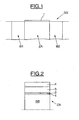
- the first step of the process of the invention ( figure 2 ) is deposited on the layer 1 of silicon oxide, in the single-plate reactor, a silicon coupling layer 2 of thickness ⁇ 1 nm, preferably about 0.5 nm, using a gas mixture with a temperature below 580 ° C.
- a gas mixture with a temperature below 580 ° C.
- a mixture of silane and hydrogen SiH 4 / H 2
- the gas flow rates used are preferably 400 cm 3 per minute for 30 seconds under standard conditions for the silane and preferably 20 to 30 liters per minute under standard conditions for hydrogen.
- the deposition temperature of the primer layer is between 500 and 580 ° C, preferably 550 ° C.
- the deposition pressure is generally atmospheric.
- this deposition step of the silicon bonding layer is that the thickness of the final bonding layer is ⁇ 1 nm, preferably of the order of 0.5 nm. Therefore, the duration of this deposition step must be determined according to other deposition conditions to ensure that the thickness of the bonding layer is less than or equal to 1 nm.
- Such a bonding layer with a thickness less than or equal to 1 nm makes it possible to obtain a deposit of a Si 1-x Ge x polycrystalline layer having a minimum particle size, of the order of 20 nm. in the most unfavorable case of a pure Ge layer of 100 nm, without affecting the electrical properties (shift of the threshold voltage V t ).
- the second step of the process according to the invention is the deposition of a layer 3 of Si 1-x Ge x where 0 ⁇ x ⁇ 1.
- x is between 0.05 and 1, more preferably between 0, 25 and 1, and more preferably between 0.50 and 1.
- the gaseous mixture generally used for CVD deposition is a mixture of silane, germane and hydrogen (SiH 4 / GeH 4 / H 2 ).
- the proportions of the different gases of the mixture vary according to the desired germanium and silicon contents for the Si 1-x Ge x layer and can be easily determined by those skilled in the art depending on the composition desired for the Si 1 layer. -x Ge x .
- the deposition is carried out at a temperature between 400 and 550 ° C, and preferably between 450 and 550 ° C.
- the deposition temperature will be between 400 and 450 ° C.
- the total deposition pressure is generally atmospheric.
- the duration of the deposition is a function of the temperature and pressure conditions, the proportions of the different gases in the gaseous mixture and the desired thickness for the Si 1-x Ge x polycrystalline layer.
- the thickness of the Si 1-x Ge x polycrystalline layer will be between 50 nm and 200 nm, preferably between 100 and 150 nm, and better between 80 and 150 nm.
- the silicon-germanium layer 3 is then deposited on second silicon layer 4 (or encapsulation layer) using a gas mixture, for example a mixture of silane and hydrogen.
- This layer generally has a thickness of 50 to 200 nm, and preferably 50 to 100 nm.
- the first phase of treatments involving the realization of the Si, Si / Ge and Si stack in a single-plate furnace makes it possible to perfectly control the nucleation of SiGe on the gate oxide, to control the uniformity of thickness and concentration. in germanium on the plate and achieve a polycrystalline SiGe / Si bilayer system without air release of the plate between the two layers.
- Monoplase deposition can control concentrations of germanium from 0 to 100% and particularly particularly useful deposits in which the concentration is greater than 50%.
- the gate must be compatible CMOS, that is to say, locally implanted N or P, depending on the type of transistor to achieve.
- CMOS complementary metal-oxide-semiconductor
- These local implantations are performed through an organic resin mask which implies a subsequent withdrawal thereof. It is precisely the removal of this resin, and the appropriate surface cleaning, that require the silicon-germanium grid to be encapsulated under a layer of silicon so as not to modify or even remove, the layer of silicon-germanium during resin removal.
- the thicknesses of the silicon-germanium (or germanium) and encapsulation silicon layer result from a compromise between the growth of silicon / germanium or germanium grains (so as to avoid heterogeneous nucleation) and that of polycrystalline silicon. encapsulation that is based on these grains.
- the silicon / germanium layer must be as continuous as possible, that is to say the least rough possible. This layer of silicon germanium must therefore be thick enough but not too much.
- the total thickness of the grid thus formed is, for example, 200 nm for a 0.18 ⁇ m technology. It will be lower for technologies smaller than 0.18 ⁇ m, typically of the order of 100 to 150 nm.
- the current compromise is a SiGe layer 120 nm thick and an encapsulation silicon layer 80 nm thick, for a technology 0.18 microns.
- the next step of the process according to the invention consists of a doping of the stack formed in the figure 2 .
- the gate will be doped P type regardless of the type of transistor, and this for theoretical reasons.
- the doping of the gate is done either by a full plate ion implantation, or in-situ during the actual deposit of the stack in the single-plate reactor using gaseous mixtures.
- a direct deposition of a doped polycrystalline Si 1-x Ge x layer for example with boron or phosphorus
- a gaseous compound of the desired doping element for example B 2 H 6 or PH 3
- the proportion of gaseous compound of the doping element in the gaseous mixture will be a function of the desired content of doping element in the deposited layer.
- the doping levels are equal to or greater than 10 17 cm -3 and preferably of the order of 10 20 cm -3.
- the direct deposition of a doped Si 1-x Ge x layer it is recommended to avoid the diffusion of the dopants in the thin layer of SiO 2 (gate oxide), to make a pre-deposit of a Si 1-x Ge x undoped prior to depositing the Si 1-x Ge x doped.
- This pre-deposition of sufficient thickness for the protection of the underlying gate oxide, is carried out as described above for the deposition of the Si 1-x Ge x layer.
- the gaseous compound of the doping element is added to the gaseous mixture to deposit the doped Si 1-x Ge x layer as indicated above.
- the deposition of the layer 4 of encapsulating silicon which can also be doped is preferably carried out in the single-plate reactor using a conventional gaseous mixture, for example a mixture of silane and hydrogen, optionally containing a gaseous compound of the doping element such as B 2 H 6 and PH 3 , under standard conditions.
- a conventional gaseous mixture for example a mixture of silane and hydrogen, optionally containing a gaseous compound of the doping element such as B 2 H 6 and PH 3 , under standard conditions.
- the etching of the grid is done after a photo-lithography step of a traditional organic resin.
- the high-density plasma etching methods conventionally used for silicon etching are not suitable for etching a layer of Si 1-x Ge x or of a Si 1-x Ge x / Si stack, in particular when the germanium content of the poly Si 1-x Ge x layer is greater than 50% (x ⁇ 0.5).
- conventional plasma etching processes lead to deformations of the profiles of the etched patterns, in particular the flanks thereof.
- the etching according to the invention begins with the formation ( figure 3 ) of a mask 5 of inorganic material, which comprises the deposition, by a conventional method such as a low-pressure vapor phase deposition, of an inorganic material, for example a SiO 2 layer or a SiO double layer 2 / SiON.
- a mask 5 of inorganic material which comprises the deposition, by a conventional method such as a low-pressure vapor phase deposition, of an inorganic material, for example a SiO 2 layer or a SiO double layer 2 / SiON.
- the mask 5 of inorganic material is etched ( figure 5 ), preferably by high density plasma etching, and more preferably using a gaseous mixture of chlorine and nitrogen and / or ammonia.
- An essential characteristic of the etching of the GR gate according to the invention ( figure 6 ) consists of an anisotropic main etching step, using a high density gas plasma based on chlorine, free of oxygen and HBr, and including N 2 or NH 3 or their mixture to produce a passivation layer of etching flanks by co-adsorption with atomic chlorine to reduce the lateral velocity of spontaneous etching by chlorine.
- This addition of N 2 or NH 3 or a mixture of these compounds causes little or no etching residue, and does not cause lateral erosion or alteration of the Si 1-x Ge x layer or the underlying gate oxide.
- the use of such a gas mixture is compatible with industrial implementations of the etching process.
- the proportions of N 2 and / or NH 3 introduced into the gaseous mixture of the plasma can be determined experimentally, in a conventional manner, and must be sufficient to block the kinetics of the spontaneous chemical reactions responsible for lateral etching of the flanks of the non-submitted etched patterns. to ionic bombardment, without blocking the kinetics of the reactions induced by the ionic bombardment responsible for vertical etching.
- the main etching step is followed by an overgrafting step in which the energy of the plasma ions is reduced compared to the main etching step.
- this step of supergrafting it is possible to use the same gaseous mixture as in the main etching step, but it is also possible to use gaseous mixtures containing oxygen, because the passivation layer formed by the flanks of the etched pattern during the main etching step with the gaseous mixture free of oxygen and HBr protects the flanks of the etched pattern of a spontaneous etching by the oxygen atoms during this step of overgrafting.
- the amount of oxygen can be determined experimentally to increase the Si 1-x Ge x / gate oxide selectivity without spontaneously etching the etched patterns.
- the main etching step is stopped before reaching the underlying silicon oxide layer 1, preferably at a distance of between 30 and 40 nm of the silicon oxide 1. This avoids any risk of degradation of the gate oxide during the main engraving step.
- a layer 1 of silicon oxide of a substrate is formed on a layer 1 and on a coupling layer 2, a stack of a first layer 3 of Si 0.45 Ge 0.55 polycrystalline (120 nm thick) and a second layer 4 of polycrystalline silicon (80 nm thick).
- a masking layer 5 is deposited in an inorganic material, for example a silicon oxide layer.
- a strong deformation of the etching profile of the patterns in the flanks of the Si 0.45 Ge 0.55 polycrystalline layer is observed.
- the passivation layer of 0.45 Ge 0.55 Si flanks is a highly chlorinated stoichiometric silicon oxide.
- the passivation layer is therefore formed only from the silicon etching reaction products, which explains why its thickness on the flank of the etched pattern decreases for the Si layer 0.45 Ge 0.55 .
- this step consists of deoxidation in a low concentration HF bath ( ⁇ 1%). Typically, this step corresponds to the etching of 10 ⁇ of thermal oxide on a full plate. It is mainly used to dissolve all polymer residues that could have been generated during the etching of the grid.
- the entire hard mask 5 It is possible, but not essential, to also remove in this step the entire hard mask 5, if the withdrawal time is compatible with the technology used. This is particularly the case with a 60 nm hard mask of SiO 2 in a 0.18 ⁇ technology. Indeed, the hard mask removal time in a dilute hydrofluoric acid bath is typically equal to the etching time of a 60 ⁇ thermal oxide.
- the next step ( figure 7 ) consists of an encapsulation of the GR gate by a non-oxidizing material 7 vis-à-vis germanium, typically a silicon oxide SiO 2 or SiON layer.
- a non-oxidizing material 7 vis-à-vis germanium typically a silicon oxide SiO 2 or SiON layer.
- This stage of encapsulation of the gate is essential to protect sidewalls of the grid during the following technological steps, which consist in particular in the realization of the implantations of the drain and source regions requiring photo-lithography steps, which, because of the need for removal of an organic resin, would damage the silicon / germanium layer.
- this encapsulating silicon oxide layer a deposition by a gaseous plasma of CVD type is used.
- a plasma oxide for this encapsulation is justified by the fact that germanium reacts very strongly with oxygen. It is therefore necessary to use a process in which the atomic oxygen has a very short gas phase lifetime, as is the case for a low-temperature plasma-enhanced chemical vapor deposition (PECVD) oxide. .
- PECVD low-temperature plasma-enhanced chemical vapor deposition
- this encapsulation layer 7 is between 5 and 10 nm. This small thickness is justified so as not to stray too far from traditional silicon technologies which use a thermal oxide with a thickness varying between 2.5 and 5 nm. On the other hand, this small thickness makes it possible to control the depth of the different implantations without altering the intrinsic electrical properties of the transistors.
- this transistor comprising the GR encapsulated gate, the conventional steps (not shown for simplification purposes) of photo-lithography and the implantation of the source and drain regions (LDD implantations for example) for the formation of the insulating lateral regions of the grid (spacers 8, figure 8 ).
- the choice of material depends on the possible thermal balance of the technological sector. This being so, since the encapsulating oxide 7, protecting the sides of the GR gate, is porous to oxygen, any deposit involving oxygen at high temperature is to be excluded, as in particular an oxidation of the temperature-assisted silicon (TEOS deposit).
- the material for the spacers may be on the other hand either a plasma oxide obtained at low temperature (SiO 2 ), or a silicon nitride Si 3 N 4.
- the typical thicknesses of the deposits are optimized according to the constraints of the technological sectors used. Typically, it is possible to deposit a layer of SiO 2 250 nm thick or a layer of Si 3 N4 100 nm thick for spacers which, after etching, have a width at the bottom of the grid of 0, 1 to 0.13 ⁇ .
- Spacer etching is a conventional step well known to those skilled in the art. It should be noted here that, if during the step of removing the polymer residues after etching of the grid, the removal of the hard mask 5, could not be possible, its removal can be carried out now either during the step dry etching of the spacers, or by selective chemical etching vis-à-vis the spacers at the end of this step.
Landscapes
- Insulated Gate Type Field-Effect Transistor (AREA)
- Chemical Vapour Deposition (AREA)
- Electrodes Of Semiconductors (AREA)
- Drying Of Semiconductors (AREA)
- Formation Of Insulating Films (AREA)
Claims (18)
- Verfahren zum Erhalt eines Si1-xGex-Isolated-Gate-Feldeffekttransistors, wobei 0 < x ≤ 1, aus einem Halbleitersubstrat (SB) mit einer sogenannten aktiven Zone (ZA) mit einer darüber angeordneten Gateoxidschicht (1), umfassend:- eine erste Phase von Behandlungen in einem Einwaferreaktor, umfassend eine Abscheidung einer Siliciumhaftschicht (2) mit einer Dicke kleiner gleich 2 nm auf der Gateoxidschicht (1) durch CVD bei einer Temperatur kleiner gleich 580°C und eine Abscheidung eines Stapels mit einer durch CVD bei einer Temperatur kleiner gleich 550°C erhaltenen ersten kontinuierlichen Schicht (3) aus Si1-xGex mit einer darüber angeordneten zweiten Siliciumschicht (4) auf der Haftschicht, dann- eine Phase der Bildung des Gate (GR) des Transistors, umfassend eine Abscheidung einer Deckschicht (5) aus einem anorganischen Material auf dem Stapel, ein erstes Ätzen der Deckschicht (5) zum Erhalt einer über dem Stapel angeordneten anorganischen Maske (5), ein zweites Ätzen des Stapels unter Verwendung der Maske zur Bildung des Gatebereichs (GR) und eine Abscheidung einer Verkapselungsschicht (7) aus einem gegenüber Germanium nichtoxidierenden Material auf dem Gatebereich, dann- eine zweite Phase von Behandlungen, umfassend die Bildung von isolierenden Seitenbereichen (8) aus einem gegenüber Germanium nichtoxidierenden Material auf den Flanken des verkapselten Gate.
- Verfahren nach Anspruch 1, dadurch gekennzeichnet, daß die Abscheidung der Haftschicht (2) bei einer Temperatur zwischen 500 und 580°C erfolgt und die Abscheidung der ersten kontinuierlichen Schicht (3) aus Si1-xGex bei einer Temperatur zwischen 400 und 500°C erfolgt.
- Verfahren nach Anspruch 1 oder 2, dadurch gekennzeichnet, daß die Haftschicht (2) eine Dicke kleiner gleich 1 nm aufweist.
- Verfahren nach einem der vorhergehenden Ansprüche, dadurch gekennzeichnet, daß das Gasgemisch für die Abscheidung der Haftschicht (2) aus einem Gemisch von Silan und Wasserstoff gebildet wird und das Gasgemisch für die Abscheidung der ersten kontinuierlichen Schicht (3) aus Si1-xGex aus einem Gemisch von Silan, German und Wasserstoff gebildet wird.
- Verfahren nach einem der vorhergehenden Ansprüche, dadurch gekennzeichnet, daß die erste Phase von Behandlungen die Dotierung des Stapels umfaßt.
- Verfahren nach Anspruch 5, dadurch gekennzeichnet, daß die Dotierung des Stapels die Einführung eines Dotierelements in das für die Abscheidung der ersten kontinuierlichen Schicht (3) aus Si1-xGex verwendete Gasgemisch nach Abscheidung einer undotierten Si1-xGex-Unterschicht umfaßt.
- Verfahren nach einem der vorhergehenden Ansprüche, dadurch gekennzeichnet, daß in der Phase der Bildung des Gate (GR) des Transistors das erste Ätzen mit einem hochdichten Plasma eines aus Cl2, N2 und/oder NH3 bestehenden Gasgemischs erfolgt.
- Verfahren nach einem der vorhergehenden Ansprüche, dadurch gekennzeichnet, daß in der Phase der Bildung des Gate des Transistors das zweite Ätzen ein anisotropes Hauptätzen umfaßt und mit einem hochdichten Plasma eines aus Cl2 und entweder N2 oder NH3 oder einem Gemisch von N2 und NH3 bestehenden Gasgemischs erfolgt.
- Verfahren nach Anspruch 8, dadurch gekennzeichnet, daß das Hauptätzen vor dem Erreichen des Gateoxids (1), vorzugsweise 30 bis 40 nm vor dem Erreichen des Gateoxids, beendet wird.
- Verfahren nach Anspruch 8 oder 9, dadurch gekennzeichnet, daß das zweite Ätzen nach dem Hauptätzen ein Überätzen mit einem hochdichten Gasplasma eines aus Cl2 und N2 oder NH3 oder einem Gemisch davon und gegebenenfalls O2 bestehenden Gasgemischs umfaßt.
- Verfahren nach einem der vorhergehenden Ansprüche, dadurch gekennzeichnet, daß die Abscheidung der Verkapselungsschicht (7) auf dem Gatebereich, über dem zumindest teilweise die anorganische Maske (5) angeordnet ist, erfolgt.
- Verfahren nach einem der vorhergehenden Ansprüche, dadurch gekennzeichnet, daß die anorganische Maske (5) aus einer SiO2-Schicht, gegebenenfalls mit darüber angeordeneter SiON-Schicht, gebildet wird.
- Verfahren nach einem der vorhergehenden Ansprüche, dadurch gekennzeichnet, daß es sich bei der Verkapselungsschicht (7) um eine mittels CVD-Gasplasma abgeschiedene SiO2- oder SiON-Schicht handelt.
- Verfahren nach Anspruch 13, dadurch gekennzeichnet, daß die Verkapselungsschicht eine Dicke zwischen 5 und 10 nm aufweist.
- Verfahren nach einem der vorhergehenden Ansprüche, dadurch gekennzeichnet, daß die isolierenden Seitenbereiche (8) aus durch Niedertemperatur-Gasplasma abgeschiedenes SiO2 oder aus Si3N4 gebildet werden.
- Verfahren nach einem der vorhergehenden Ansprüche, dadurch gekennzeichnet, daß die Gateoxidschicht (1) in dem Einwaferreaktor abgeschieden wird.
- Verfahren nach einem der vorhergehenden Ansprüche, dadurch gekennzeichnet, daß x zwischen 0,5 und 1 liegt.
- Verfahren nach einem der vorhergehenden Ansprüche, dadurch gekennzeichnet, daß die erste kontinuierliche Schicht (3) aus Si1-xGex eine Dicke zwischen 50 und 200 nm aufweist und die zweite Siliciumschicht (4) eine Dicke zwischen 50 und 200 nm aufweist.
Applications Claiming Priority (2)
| Application Number | Priority Date | Filing Date | Title |
|---|---|---|---|
| FR9707938A FR2765394B1 (fr) | 1997-06-25 | 1997-06-25 | Procede d'obtention d'un transistor a grille en silicium-germanium |
| FR9707938 | 1997-06-25 |
Publications (2)
| Publication Number | Publication Date |
|---|---|
| EP0887843A1 EP0887843A1 (de) | 1998-12-30 |
| EP0887843B1 true EP0887843B1 (de) | 2010-09-15 |
Family
ID=9508412
Family Applications (1)
| Application Number | Title | Priority Date | Filing Date |
|---|---|---|---|
| EP98401432A Expired - Lifetime EP0887843B1 (de) | 1997-06-25 | 1998-06-12 | Verfahren zur Herstellung eines Transistors mit einem Silizium-Germanium-Gatter |
Country Status (5)
| Country | Link |
|---|---|
| US (1) | US5998289A (de) |
| EP (1) | EP0887843B1 (de) |
| JP (1) | JP4601734B2 (de) |
| DE (1) | DE69841896D1 (de) |
| FR (1) | FR2765394B1 (de) |
Families Citing this family (44)
| Publication number | Priority date | Publication date | Assignee | Title |
|---|---|---|---|---|
| FR2765393B1 (fr) * | 1997-06-25 | 2001-11-30 | France Telecom | Procede de gravure d'une couche de si1-xgex polycristallin ou d'un empilement d'une couche de si1-xgex polycristallin et d'une couche de si polycristallin, et son application a la microelectronique |
| US6180499B1 (en) * | 1998-09-29 | 2001-01-30 | Advanced Micro Devices, Inc. | Method for forming polysilicon-germanium gate in CMOS transistor and device made thereby |
| JP3616514B2 (ja) * | 1998-11-17 | 2005-02-02 | 株式会社東芝 | 半導体集積回路及びその製造方法 |
| KR100881472B1 (ko) | 1999-02-04 | 2009-02-05 | 어플라이드 머티어리얼스, 인코포레이티드 | 소정 기판 상에 놓여져 있는 패턴화된 마스크 표면 위로 적층 구조물을 증착하기 위한 방법 |
| US6197673B1 (en) * | 1999-06-08 | 2001-03-06 | United Semiconductor Corp. | Method of fabricating passivation of gate electrode |
| WO2000079601A1 (fr) * | 1999-06-23 | 2000-12-28 | Seiko Epson Corporation | Dispositif a semi-conducteur et procede de fabrication dudit dispositif |
| US6441464B1 (en) * | 1999-09-22 | 2002-08-27 | International Business Machines Corporation | Gate oxide stabilization by means of germanium components in gate conductor |
| KR100336572B1 (ko) * | 1999-11-04 | 2002-05-16 | 박종섭 | 폴리 실리콘-저마늄을 게이트 전극으로 사용하는 반도체소자의 형성방법 |
| US6373112B1 (en) * | 1999-12-02 | 2002-04-16 | Intel Corporation | Polysilicon-germanium MOSFET gate electrodes |
| WO2001041544A2 (en) * | 1999-12-11 | 2001-06-14 | Asm America, Inc. | Deposition of gate stacks including silicon germanium layers |
| EP1246258B1 (de) | 2000-01-07 | 2011-02-23 | Sharp Kabushiki Kaisha | Halbleiteranordnung und informationsverarbeitungsanordnung |
| KR100587053B1 (ko) * | 2000-06-30 | 2006-06-07 | 주식회사 하이닉스반도체 | 반도체 소자의 제조방법 |
| US6399469B1 (en) * | 2000-07-10 | 2002-06-04 | Advanced Micro Devices, Inc. | Fabrication of a notched gate structure for a field effect transistor using a single patterning and etch process |
| US6423632B1 (en) | 2000-07-21 | 2002-07-23 | Motorola, Inc. | Semiconductor device and a process for forming the same |
| US6891235B1 (en) | 2000-11-15 | 2005-05-10 | International Business Machines Corporation | FET with T-shaped gate |
| KR100425934B1 (ko) | 2000-12-29 | 2004-04-03 | 주식회사 하이닉스반도체 | 실리콘-게르마늄막 형성 방법 |
| AU2002306436A1 (en) | 2001-02-12 | 2002-10-15 | Asm America, Inc. | Improved process for deposition of semiconductor films |
| US7026219B2 (en) | 2001-02-12 | 2006-04-11 | Asm America, Inc. | Integration of high k gate dielectric |
| US6432763B1 (en) * | 2001-03-15 | 2002-08-13 | Advanced Micro Devices, Inc. | Field effect transistor having doped gate with prevention of contamination from the gate during implantation |
| FR2823009B1 (fr) * | 2001-04-02 | 2004-07-09 | St Microelectronics Sa | Procede de fabrication d'un transistor vertical a grille isolee a faible recouvrement de la grille sur la source et sur le drain, et circuit integre comportant un tel transistor |
| KR20030002759A (ko) * | 2001-06-29 | 2003-01-09 | 주식회사 하이닉스반도체 | 반도체 소자의 트랜지스터 제조 방법 |
| US6952040B2 (en) * | 2001-06-29 | 2005-10-04 | Intel Corporation | Transistor structure and method of fabrication |
| US6566210B2 (en) * | 2001-07-13 | 2003-05-20 | International Business Machines Corporation | Method of improving gate activation by employing atomic oxygen enhanced oxidation |
| US6730588B1 (en) * | 2001-12-20 | 2004-05-04 | Lsi Logic Corporation | Method of forming SiGe gate electrode |
| KR100487525B1 (ko) * | 2002-04-25 | 2005-05-03 | 삼성전자주식회사 | 실리콘게르마늄 게이트를 이용한 반도체 소자 및 그 제조방법 |
| US7186630B2 (en) | 2002-08-14 | 2007-03-06 | Asm America, Inc. | Deposition of amorphous silicon-containing films |
| AU2003284272A1 (en) * | 2002-10-18 | 2004-05-04 | Applied Materials, Inc. | A film stack having a silicon germanium layer and a thin amorphous seed layer |
| US6686637B1 (en) * | 2002-11-21 | 2004-02-03 | International Business Machines Corporation | Gate structure with independently tailored vertical doping profile |
| US6838695B2 (en) * | 2002-11-25 | 2005-01-04 | International Business Machines Corporation | CMOS device structure with improved PFET gate electrode |
| US6780741B2 (en) | 2003-01-08 | 2004-08-24 | Taiwan Semiconductor Manufacturing Company, Ltd. | Method of forming a novel gate electrode structure comprised of a silicon-germanium layer located between random grained polysilicon layers |
| US7229919B2 (en) * | 2003-01-08 | 2007-06-12 | Taiwan Semiconductor Manufacturing Company, Ltd. | Semiconductor device having a random grained polysilicon layer and a method for its manufacture |
| US6905976B2 (en) * | 2003-05-06 | 2005-06-14 | International Business Machines Corporation | Structure and method of forming a notched gate field effect transistor |
| JP3742906B2 (ja) * | 2003-05-08 | 2006-02-08 | シャープ株式会社 | 半導体装置の製造方法 |
| US7199011B2 (en) * | 2003-07-16 | 2007-04-03 | Texas Instruments Incorporated | Method to reduce transistor gate to source/drain overlap capacitance by incorporation of carbon |
| JP2005079310A (ja) * | 2003-08-29 | 2005-03-24 | Semiconductor Leading Edge Technologies Inc | 半導体装置及びその製造方法 |
| US20050199872A1 (en) * | 2004-03-10 | 2005-09-15 | Tokyo Electron Limited Of Tbs Broadcast Center | Silicon-germanium thin layer semiconductor structure with variable silicon-germanium composition and method of fabrication |
| US7682985B2 (en) * | 2004-03-17 | 2010-03-23 | Lam Research Corporation | Dual doped polysilicon and silicon germanium etch |
| US7135391B2 (en) * | 2004-05-21 | 2006-11-14 | International Business Machines Corporation | Polycrystalline SiGe junctions for advanced devices |
| JP5848862B2 (ja) * | 2004-06-25 | 2016-01-27 | アプライド マテリアルズ インコーポレイテッドApplied Materials,Incorporated | カプセル化膜の遮水性能の改善 |
| US7157341B2 (en) * | 2004-10-01 | 2007-01-02 | International Business Machines Corporation | Gate stacks |
| US20070155138A1 (en) * | 2005-05-24 | 2007-07-05 | Pierre Tomasini | Apparatus and method for depositing silicon germanium films |
| JP2007019400A (ja) * | 2005-07-11 | 2007-01-25 | Renesas Technology Corp | Mos構造を有する半導体装置およびその製造方法 |
| CN102692682B (zh) * | 2012-06-12 | 2013-07-17 | 中国科学院上海微系统与信息技术研究所 | 一种光栅耦合器及其制作方法 |
| CN118156133A (zh) * | 2022-12-05 | 2024-06-07 | 上海华力集成电路制造有限公司 | 全耗尽型绝缘体上硅pmos器件制造方法 |
Family Cites Families (9)
| Publication number | Priority date | Publication date | Assignee | Title |
|---|---|---|---|---|
| US5019882A (en) * | 1989-05-15 | 1991-05-28 | International Business Machines Corporation | Germanium channel silicon MOSFET |
| US5155571A (en) * | 1990-08-06 | 1992-10-13 | The Regents Of The University Of California | Complementary field effect transistors having strained superlattice structure |
| US5241214A (en) * | 1991-04-29 | 1993-08-31 | Massachusetts Institute Of Technology | Oxides and nitrides of metastabale group iv alloys and nitrides of group iv elements and semiconductor devices formed thereof |
| US5461250A (en) * | 1992-08-10 | 1995-10-24 | International Business Machines Corporation | SiGe thin film or SOI MOSFET and method for making the same |
| US5354700A (en) * | 1993-07-26 | 1994-10-11 | United Microelectronics Corporation | Method of manufacturing super channel TFT structure |
| US5461243A (en) * | 1993-10-29 | 1995-10-24 | International Business Machines Corporation | Substrate for tensilely strained semiconductor |
| JPH07202178A (ja) * | 1993-12-28 | 1995-08-04 | Toshiba Corp | 半導体装置およびその製造方法 |
| US5985703A (en) * | 1994-10-24 | 1999-11-16 | Banerjee; Sanjay | Method of making thin film transistors |
| JPH08186256A (ja) * | 1994-12-29 | 1996-07-16 | Sony Corp | Ldd構造のトランジスタの製造方法及びトランジスタ |
-
1997
- 1997-06-25 FR FR9707938A patent/FR2765394B1/fr not_active Expired - Lifetime
-
1998
- 1998-06-12 EP EP98401432A patent/EP0887843B1/de not_active Expired - Lifetime
- 1998-06-12 DE DE69841896T patent/DE69841896D1/de not_active Expired - Lifetime
- 1998-06-23 US US09/102,849 patent/US5998289A/en not_active Expired - Lifetime
- 1998-06-25 JP JP17874998A patent/JP4601734B2/ja not_active Expired - Lifetime
Also Published As
| Publication number | Publication date |
|---|---|
| FR2765394A1 (fr) | 1998-12-31 |
| JPH1187708A (ja) | 1999-03-30 |
| JP4601734B2 (ja) | 2010-12-22 |
| DE69841896D1 (de) | 2010-10-28 |
| EP0887843A1 (de) | 1998-12-30 |
| US5998289A (en) | 1999-12-07 |
| FR2765394B1 (fr) | 1999-09-24 |
Similar Documents
| Publication | Publication Date | Title |
|---|---|---|
| EP0887843B1 (de) | Verfahren zur Herstellung eines Transistors mit einem Silizium-Germanium-Gatter | |
| EP0780889B1 (de) | Verfahren zur selektiven Abscheidung von Siliciden hochschmelzender Metalle auf Silizium | |
| FR2900276A1 (fr) | Depot peald d'un materiau a base de silicium | |
| US7625807B2 (en) | Methods and systems to mitigate etch stop clipping for shallow trench isolation fabrication | |
| EP3144973B1 (de) | Verfahren zur bildung von abstandhaltern eines gates eines transistors | |
| US6225171B1 (en) | Shallow trench isolation process for reduced for junction leakage | |
| EP3261124B1 (de) | Verfahren zur bildung von abstandhaltern eines gates eines transistors | |
| EP0976149B1 (de) | Verfahren zur verminderung der interdiffusion in einem halbleiterbauelement mit si/sige verbindungs-gatter | |
| EP3174092B1 (de) | Verfahren zur bildung von abstandhaltern eines gates eines transistors | |
| EP3376545B1 (de) | Transistor mit strukturierten source- und drain-bereichen, und sein bearbeitungsverfahren | |
| FR3116940A1 (fr) | Procédé basse température de fabrication d’un substrat semiconducteur sur isolant | |
| EP2975634B1 (de) | Verfahren zur bildung von kontaktöffnungen für einen transistor | |
| EP0905759B1 (de) | Verfahren zum Ätzen einer aus Si1-xGex polykristallinen Schicht oder einer aus polykristallinen Si1-xGex/Si Stapelschicht, und Verwendung in der Herstellung von elektronischen Anordnungen | |
| FR3047352A1 (fr) | Procede de fabrication d'un transistor a dopant localise a l'aplomb de la grille | |
| US7795151B2 (en) | Methods of forming a trench having side surfaces including a uniform slope | |
| FR3068506A1 (fr) | Procede pour preparer un support pour une structure semi-conductrice | |
| JPH11288932A (ja) | 高品質窒化珪素の高速蒸着 | |
| EP3107124B1 (de) | Verfahren zur bildung von abstandshaltern eines gates eines transistors | |
| FR2853452A1 (fr) | Procede de fabrication d'un dispositif semiconducteur comprenant un dielectrique de grille en materiau a haute permittivite dielectrique | |
| FR2765245A1 (fr) | Procede d'obtention d'une couche de silicium-germanium polycristallin sur un substrat et son application a la microelectronique | |
| EP3136429B1 (de) | Herstellung von ohmschen kontakten für eine vorrichtung, die einen bereich aus iii-v-halbleitermaterial und einen bereich aus einem anderen halbleitermaterial enthält | |
| FR2805924A1 (fr) | Procede de gravure d'une couche de silicium polycristallin et son application a la realisation d'un emetteur auto- aligne avec la base extrinseque d'un transistor bipolaire simple ou double polysilicium | |
| WO1991000615A1 (fr) | Procede de fabrication de l'oxyde de champ d'un circuit integre sur du silicium | |
| FR3164834A1 (fr) | Procédé de réalisation d’un dispositif à transistors CFET | |
| FR3164835A1 (fr) | Procédé de réalisation d’un dispositif à transistors CFET |
Legal Events
| Date | Code | Title | Description |
|---|---|---|---|
| PUAI | Public reference made under article 153(3) epc to a published international application that has entered the european phase |
Free format text: ORIGINAL CODE: 0009012 |
|
| AK | Designated contracting states |
Kind code of ref document: A1 Designated state(s): BE DE FR GB IE IT NL |
|
| AX | Request for extension of the european patent |
Free format text: AL;LT;LV;MK;RO;SI |
|
| 17P | Request for examination filed |
Effective date: 19990526 |
|
| AKX | Designation fees paid |
Free format text: BE DE FR GB IE IT NL |
|
| RAP1 | Party data changed (applicant data changed or rights of an application transferred) |
Owner name: FAHRENHEIT THERMOSCOPE LLC |
|
| GRAP | Despatch of communication of intention to grant a patent |
Free format text: ORIGINAL CODE: EPIDOSNIGR1 |
|
| GRAS | Grant fee paid |
Free format text: ORIGINAL CODE: EPIDOSNIGR3 |
|
| GRAA | (expected) grant |
Free format text: ORIGINAL CODE: 0009210 |
|
| AK | Designated contracting states |
Kind code of ref document: B1 Designated state(s): BE DE FR GB IE IT NL |
|
| REG | Reference to a national code |
Ref country code: GB Ref legal event code: FG4D Free format text: NOT ENGLISH |
|
| REG | Reference to a national code |
Ref country code: IE Ref legal event code: FG4D Free format text: LANGUAGE OF EP DOCUMENT: FRENCH |
|
| REF | Corresponds to: |
Ref document number: 69841896 Country of ref document: DE Date of ref document: 20101028 Kind code of ref document: P |
|
| REG | Reference to a national code |
Ref country code: NL Ref legal event code: VDEP Effective date: 20100915 |
|
| REG | Reference to a national code |
Ref country code: IE Ref legal event code: FD4D |
|
| PG25 | Lapsed in a contracting state [announced via postgrant information from national office to epo] |
Ref country code: IE Free format text: LAPSE BECAUSE OF FAILURE TO SUBMIT A TRANSLATION OF THE DESCRIPTION OR TO PAY THE FEE WITHIN THE PRESCRIBED TIME-LIMIT Effective date: 20100915 |
|
| PG25 | Lapsed in a contracting state [announced via postgrant information from national office to epo] |
Ref country code: IT Free format text: LAPSE BECAUSE OF FAILURE TO SUBMIT A TRANSLATION OF THE DESCRIPTION OR TO PAY THE FEE WITHIN THE PRESCRIBED TIME-LIMIT Effective date: 20100915 Ref country code: NL Free format text: LAPSE BECAUSE OF FAILURE TO SUBMIT A TRANSLATION OF THE DESCRIPTION OR TO PAY THE FEE WITHIN THE PRESCRIBED TIME-LIMIT Effective date: 20100915 |
|
| PLBE | No opposition filed within time limit |
Free format text: ORIGINAL CODE: 0009261 |
|
| STAA | Information on the status of an ep patent application or granted ep patent |
Free format text: STATUS: NO OPPOSITION FILED WITHIN TIME LIMIT |
|
| 26N | No opposition filed |
Effective date: 20110616 |
|
| REG | Reference to a national code |
Ref country code: DE Ref legal event code: R097 Ref document number: 69841896 Country of ref document: DE Effective date: 20110616 |
|
| BERE | Be: lapsed |
Owner name: FAHRENHEIT THERMOSCOPE LLC Effective date: 20110630 |
|
| PG25 | Lapsed in a contracting state [announced via postgrant information from national office to epo] |
Ref country code: BE Free format text: LAPSE BECAUSE OF NON-PAYMENT OF DUE FEES Effective date: 20110630 |
|
| REG | Reference to a national code |
Ref country code: FR Ref legal event code: PLFP Year of fee payment: 19 |
|
| REG | Reference to a national code |
Ref country code: FR Ref legal event code: PLFP Year of fee payment: 20 |
|
| PGFP | Annual fee paid to national office [announced via postgrant information from national office to epo] |
Ref country code: FR Payment date: 20170518 Year of fee payment: 20 Ref country code: GB Payment date: 20170526 Year of fee payment: 20 |
|
| PGFP | Annual fee paid to national office [announced via postgrant information from national office to epo] |
Ref country code: DE Payment date: 20170623 Year of fee payment: 20 |
|
| REG | Reference to a national code |
Ref country code: DE Ref legal event code: R071 Ref document number: 69841896 Country of ref document: DE |
|
| REG | Reference to a national code |
Ref country code: GB Ref legal event code: PE20 Expiry date: 20180611 |
|
| PG25 | Lapsed in a contracting state [announced via postgrant information from national office to epo] |
Ref country code: GB Free format text: LAPSE BECAUSE OF EXPIRATION OF PROTECTION Effective date: 20180611 |