EP0908936A2 - Formation of a bottle shaped trench - Google Patents
Formation of a bottle shaped trench Download PDFInfo
- Publication number
- EP0908936A2 EP0908936A2 EP98307809A EP98307809A EP0908936A2 EP 0908936 A2 EP0908936 A2 EP 0908936A2 EP 98307809 A EP98307809 A EP 98307809A EP 98307809 A EP98307809 A EP 98307809A EP 0908936 A2 EP0908936 A2 EP 0908936A2
- Authority
- EP
- European Patent Office
- Prior art keywords
- etching
- trench
- pressure
- temperature
- etch
- Prior art date
- Legal status (The legal status is an assumption and is not a legal conclusion. Google has not performed a legal analysis and makes no representation as to the accuracy of the status listed.)
- Granted
Links
Images
Classifications
-
- H—ELECTRICITY
- H10—SEMICONDUCTOR DEVICES; ELECTRIC SOLID-STATE DEVICES NOT OTHERWISE PROVIDED FOR
- H10P—GENERIC PROCESSES OR APPARATUS FOR THE MANUFACTURE OR TREATMENT OF DEVICES COVERED BY CLASS H10
- H10P50/00—Etching of wafers, substrates or parts of devices
- H10P50/20—Dry etching; Plasma etching; Reactive-ion etching
- H10P50/24—Dry etching; Plasma etching; Reactive-ion etching of semiconductor materials
- H10P50/242—Dry etching; Plasma etching; Reactive-ion etching of semiconductor materials of Group IV materials
Definitions
- a method for forming a bottle shaped trench in a semiconductor substrate is described herein. More particularly, a bottle shaped trench is formed in a semiconductor substrate using a single etch process by varying the etch conditions.
- reactive ion etching is a method which first creates a plasma gas composition in a reaction chamber by a radio frequency (RF) energy field.
- the plasma gas composition will usually contain neutrals, radicals and ions. The latter can be accelerated by the electric field toward the surface of the semiconductor substrate. Radicals reach the semiconductor surface by diffusion. Upon colliding with the surface of the semiconductor device, the accelerated ions together with the radicals remove material from the exposed surface of the semiconductor device.
- a sidewall passivating film normally forms from the reaction between the intermediate products or volatile by-products with species from the mask material or the process gases. This film tends to inhibit etching, shrink the physical size of the mask opening and thereby affect trench shape.
- a method forms a bottle shaped trench by (1) forming a trench by conventional DT silicon reactive ion etching; (2) forming a collar oxide at the upper portion of the trench by selective oxidation; (3) depositing into the trench in-situ phosphorous doped polysilicon; (4) annealing phosphorous dope into the trench sidewall at the bottom portion of the trench; and (5) removing the polysilicon by chemical dry etching to enlarge the diameter of the bottom portion of the trench.
- the method of this invention enables the formation of bottle shaped trenches during the deep trench etch process.
- the first etch step is carried out at a first temperature
- the second etch step is carried out at a second, higher, temperature
- the first etch step is conducted at a first pressure and etching is continued at a second pressure that is less than the first pressure.
- the invention relates to the formation of a bottle shaped trench which may be used to form a trench capacitor employed in an integrated circuit (IC).
- IC may be, for example, a random access memory (RAM), a dynamic random access memory (DRAM), a synchronous DRAM (SDRAM), and a read only memory (ROM).
- RAM random access memory
- DRAM dynamic random access memory
- SDRAM synchronous DRAM
- ROM read only memory
- Other IC such as an application specific IC (ASIC), a merged DRAM-logic circuit (embedded DRAM), or any other logic circuit is also useful.
- ASIC application specific IC
- merged DRAM-logic circuit embedded DRAM
- ICs are formed on the wafer in parallel. After processing is finished, the wafer is diced to separate the ICs to individual chips. The chips are then packaged, resulting in a final product that is used in, for example, consumer products such as computer systems, cellular phones, personal digital assistants (PDAs), and other electronic products.
- PDAs personal digital assistants
- the bottle shaped trench is formed using a single two stage etch process.
- the first stage forms an upper portion of the trench and the second stage forms a bottom portion, wherein the bottom portion is formed by varying the etch parameters to result in a reentrant or bottle shaped profile.
- the fabrication of the semiconductor device is typically conducted in successive stages, one or more of which can involve depositing of desired layers of selected material onto a substrate, such as a silicon wafer using techniques known to those skilled in the art.
- a substrate such as a silicon wafer using techniques known to those skilled in the art.
- Other substrates such as gallium arsenide, germanium, silicon on insulator (SOI), or other semiconductor materials are also useful.
- the substrate for example, may be lightly or heavily doped wich dopants of a predetermined conductivity to achieve the desired electrical characteristics.
- a pad stack is formed on the substrate.
- the pad stack are those typically used to form deep trenches.
- Such a pad stack includes, for example, a silicon nitride layer 12 is deposited on silicon wafer 10 and a dielectric layer (e.g., TEOS) layer 14 is deposited upon layer 12.
- layers 12 and 14 will form a hard mask for the deep trench etching step.
- the nitride layer serves as a polish stop layer for subsequent polish steps.
- an oxide layer (not shown) is provided therebetween.
- a resist layer (not shown) can be formed in a pattern on the surface of the semiconductor device by microlithographic techniques. Forming a pattern typically involves coating at least a portion of the semiconductor device with a resist material and then exposing in the appropriate pattern.
- the resist can then be developed in accordance with methods well known in the art to remove either the exposed or unexposed portions, depending on whether a positive or negative resist is used. Once the resist is developed, subsequent processing steps then can be performed to locally impact the appropriate physical changes, e.g., a bottle shaped trench of which the method for forming will be described herein, in the semiconductor material to yield a desired device structure.
- Materials and methods suitable for forming and patterning the resist layer as well as developer compositions are known to those skilled in the art. Such conventional materials can be used herein.
- the semiconductor device can be subjected to an etching method, e.g., reactive ion etching, plasma etching, etc., to perform the mask open etch, i.e., transfer the resist pattern into the TEOS 14 and the nitride layer 12 (hard mask).
- the semiconductor device can be subjected to etching to form the bottle shaped trench of this invention.
- a reactive ion etch for example, may be employed to form the bottle shaped trench in a semiconductor device.
- Other anisotropic etch techniques are also useful.
- a reactive ion etch is conducted in two stages, each stage being conducted with different parameters. Parameters that can be varied include, for example, radio frequency power, reaction chamber pressure, backfilling pressure, and such like, as described hereinbelow.
- the reactive ion etch parameters are adjusted such that the first stage advantageously forms a trench having a tapered top portion 25 and the second stage will advantageously expand the lower portion of the trench to form the bottle shaped trench.
- the tapered sidewall profile facilitates filling of the trench with materials such as pclysilicon without voids and seams in the tapered portion of the trench.
- the substrate is placed on a chuck (not shown) in a reaction chamber (not shown).
- the reaction chamber can be any conventional reaction chamber known to one skilled in the art.
- an inert gas e.g., helium, argon, etc.
- the gas promotes the cooling mechanism for the semiconductor device.
- the backfilling pressure during the first stage etching will ordinarily range from about 5 torr to about 15 torr and preferably from about 7 torr to about 10 torr. Techniques for controlling the backfilling pressure are within the purview of one skilled in the art.
- a plasma gas composition is introduced into the reaction chamber.
- the reaction chamber will be substantially free of all impurities before introducing the plasma gas composition into the reaction chamber by employing, e.g., a vacuum.
- Suitable plasma gas compositions for this invention include any conventional plasma gas composition known to one skilled in the art.
- a preferred plasma gas composition includes HBr, NF 3 and either a premixed He/O 2 or pure O 2 .
- Particularly useful plasma gas compositions have a relative concentration of from about 69% to about 90% volume percent for HBr, of from about 7.2 to about 20.0 volume percent for NF 3 and of from about 0 to about 6 volume percent for O 2 .
- a native oxide might form upon exposure of the wafer to the atmosphere after the mask open etch. Thus, it might be necessary to employ initial etch conditions that will break through any native oxide that might be present.
- the plasma gas composition will by subjected to radio frequency (RF) energy to generate ions and/or radicals.
- RF radio frequency
- the power of the RF energy employed to generate ions during the first stage of the deep etch will ordinarily range from about 400 watts to about 1000 watts and preferably from about 600 watts to about 900 watts.
- a magnetic field is generated within the reaction chamber to densify the plasma.
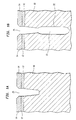
- the magnetic field strength employed during the first stage etching can range from about 15 gauss to about 170 gauss and preferably from about 100 gauss to about 170 gauss. Referring to FIG. 1A, the ions bombard the patterned areas of the resist layer on the frontside of the semiconductor device to form a trench.
- a tapered top portion 25 is formed on the trench.
- a sidewall passivation film will begin to form in the trench 20 during the bombardment of the ions on the semiconductor device.
- the rate at which the passivation film is formed determines the tapered profile of the trench.
- the reaction chamber pressure employed during the first stage etching will ordinarily range from about 20 mtorr to about 175 mtorr and preferably from about 110 mtorr to about 150 mtorr.
- the temperature of the semiconductor device during the first stage etch should be maintained in the range from about 20°C to about 100°C and preferably from about 50°C to about 90°C. Techniques for measuring and monitoring the temperature of the semiconductor device and for controlling the various other parameters to form a desired trench profile in the upper portion are within the purview of one skilled in the art.
- the first stage of the reactive ion etching method will form a trench having a tapered top portion 25.
- the first stage etch will normally be conducted for a time period ranging from about 60 seconds to about 180 seconds and preferably from about 110 seconds to about 125 seconds.
- the depth of the trench formed during the first stage etch can ordinarily range from about 1 ⁇ m to about 2 ⁇ m and preferably from about 1.25 ⁇ m to about 1.75 ⁇ m. It is to be understood that at the completion of the first stage of the deep trench etch only the tapered top portion 25 is generated having a preferred depth of about 1.5 ⁇ m. Of course the actual depth of the trench formed during the first stage depends on design parameters.
- second stage etch conditions are chosen which impart a reentrant profile or bottle shape 22 to the trench 20 (See FIG. 1B).
- the second stage etch may be initiated by increasing the temperature of the surface of the semiconductor device or decreasing the pressure within the reaction chamber, or both.
- the rate at which the sidewall passivation film is formed In the trench 20 will be reduced to a level sufficient to allow for some degree of lateral reactive ion etching in addition to the predetermined vertical reactive ion etching.
- the temperature is typically increased by about 80°C compared to the first stage temperature, so that the second stage etch is conducted at a temperature in the range of from about 100°C to about 180°C, preferably from about 130°C to about 150°C, and more preferably from about 138°C to about 142°C.
- the temperature of the semiconductor device can be increased in any manner. In particularly useful embodiments, the temperature is increased by decreasing the backfilling pressure, or increasing the RF power or both.
- the gas introduced into the gap between the frontside of the chuck and the backside of the semiconductor device controls the cooling of the semiconductor device:
- the heat transfer between the backside of the wafer and the frontside of the chuck can be modulated by varying the He backfilling pressure, thus the wafer surface temperature can be rapidly adjusted.
- the backfilling pressure is increased, the temperature of the semiconductor device is decreased and as the backfilling pressure is decreased the temperature of the semiconductor device is increased.
- the backfilling pressure can be decreased by about 50 to 100%, preferably by about 75% for a Magnetically Enhanced Reactive Ion Etching (MERIE) and 100% for Dipole Ring Magnetic etching (DRM) compared to the backfilling pressure used during the first stage etch.
- the backfilling pressure will range from about 1.5 torr to about 2.5 torr with a preferable setting of about 2 torr for the MERIE case and about 0 torr for the DRM case.
- the RF power can be increased by about 10 to about 40%, preferably about 37% for the MERIE case and about 11% for the DRM case compared to the RF power settings used during the first stage etch. Accordingly, during the second stage etch, the RF power can range from about 900 watts to about 1500 watts and preferably from about 1000 watts to about 1100 watts.
- a reduction in chamber pressure going from the first stage etching to the second stage etching is employed to change the ion angular and ion energy distributions.
- the ions With reduced pressure the ions will reflect off the tapered top portion 25 of the trench 20 to bombard the sidewalls of the trench 20 below the tapered top portion 25. Since the rate of forming the sidewall passivation film in the trench 20 has been reduced, the ions can then etch the material of the sidewall of the trench 20 to advantageously form the bottle shaped trench in the semiconductor device.
- the reaction chamber pressure can ordinarily be decreased by an amount ranging from about 15 mtorr to about 65 mtorr and preferably from about 30 mtorr to about 50 mtorr.
- the time sufficient to etch the bottle shape 22 of trench 20 in the semiconductor device after completion of the first stage etch can range from about 200 seconds to about 320 seconds and preferably from about 275 seconds to about 290 seconds.
- the overall time for the two stage etch employed in the method described herein will range from about 260 seconds to about 500 seconds.
- DRM Dipole Ring Magnetic
Landscapes
- Drying Of Semiconductors (AREA)
- Semiconductor Memories (AREA)
Abstract
Description
| Break Through | First Stage Conditions (Formation of Trench with Top Tapered Portion) | Transition Period | Second Stage Conditions (Formation of Bottle Shaped Trench) | |
| Reaction Chamber Pressure (mtorr) | 20 | 110 | 110 | 110 |
| HBr (sccm) | 20 | 55 | 55 | 55 |
| NF3 (sccm) | 5 | 8 | 8 | 8 |
| He/O2 (sccm) | 0 | 15 | 10 | 7 |
| RF Power (watt) | 600 | 800 | 800 | 1100 |
| Magnetic Field Strength (gauss) | 15 | 100 | 100 | 75 |
| He Backfilling Pressure (torr) | 8 | 8 | 4 | 2 |
| Etch Time (sec) | 25 | 100 | 25 | 250 |
| Break Through | First Stage Conditions (Formation of Trench with Top Tapered Portion) | Transition Period | Second Stage Conditions (Formation of Bottle Shaped Trench) | |
| Reaction Chamber Pressure (mtorr) | 150 | 150 | 150 | 150 |
| HBr (sccm) | 75 | 150 | 150 | 150 |
| NF3 (sccm) | 8 | 14.5 | 12 | 13 |
| O2 (sccm) | 0 | 6 | 4 | 6 |
| RF Power (watt) | 900 | 900 | 900 | 1000 |
| He Backfilling Pressure (torr) | 10/40 | 10/40 | 4/15 | 0/0 |
| Etch Time (sec) | 5 | 105 | 20 | 270 |
Claims (12)
- A method for forming in a substrate a bottle shaped trench having a tapered top portion and a wider bottom portion comprising:first etching using first etch process parameter to form a trench in the substrate having a tapered top portion; andsecond etching using second etch process parameters to form the bottom portion of the bottle shaped trench.
- The method of claim 1 wherein the first etching is carried out at a first temperature, and the second etching is carried out at a second temperature which is higher than the first temperature.
- The method of claim 2 wherein both the first and second etchings comprise plasma etching.
- The method of claim 2 wherein both the first and second etchings comprise reactive ion etching.
- The method of claim 4 wherein the second temperature is provided by reducing backfilling pressure.
- The method of claim 5 wherein backfilling pressure is reduced by about one order of magnitude from the first etching to the second etching.
- The method of claim 5 wherein backfilling pressure is reduced from about 10 torr during the first etching to about 1 torr during the second etching.
- The method of one of claims 4-7 wherein during the second etching, the second temperature is provided by increasing RF power.
- The method of claim 8 wherein RF power is increased by an amount from between 35% and 45% from the first etching to the second etching.
- The method of any preceding claim, wherein the first etching is carried out at a first pressure and the second etching is carried out at a second pressure, the second pressure being lower than the first pressure.
- The method of claim 10 wherein the second pressure is from about 30 to 50 mtorr lower than the first pressure.
- The method of claim 1 wherein the second temperature is from about 52 to about 88 degrees higher than the first temperature.
Applications Claiming Priority (2)
| Application Number | Priority Date | Filing Date | Title |
|---|---|---|---|
| US08/937,526 US5891807A (en) | 1997-09-25 | 1997-09-25 | Formation of a bottle shaped trench |
| US937526 | 1997-09-25 |
Publications (3)
| Publication Number | Publication Date |
|---|---|
| EP0908936A2 true EP0908936A2 (en) | 1999-04-14 |
| EP0908936A3 EP0908936A3 (en) | 2000-10-18 |
| EP0908936B1 EP0908936B1 (en) | 2007-06-27 |
Family
ID=25470033
Family Applications (1)
| Application Number | Title | Priority Date | Filing Date |
|---|---|---|---|
| EP98307809A Expired - Lifetime EP0908936B1 (en) | 1997-09-25 | 1998-09-25 | Formation of a bottle shaped trench |
Country Status (7)
| Country | Link |
|---|---|
| US (1) | US5891807A (en) |
| EP (1) | EP0908936B1 (en) |
| JP (1) | JPH11162949A (en) |
| KR (1) | KR100500559B1 (en) |
| CN (1) | CN1171286C (en) |
| DE (1) | DE69837981T2 (en) |
| TW (1) | TW430923B (en) |
Cited By (8)
| Publication number | Priority date | Publication date | Assignee | Title |
|---|---|---|---|---|
| EP0964456A3 (en) * | 1998-06-09 | 2000-08-09 | Siemens Aktiengesellschaft | Deep trench capacitor |
| WO2001003181A1 (en) * | 1999-06-30 | 2001-01-11 | Infineon Technologies Ag | Method for etching capacitor trenches |
| US6274457B1 (en) * | 1997-08-28 | 2001-08-14 | Mitsubishi Denki Kabushiki Kaisha | Method for manufacturing an isolation trench having plural profile angles |
| DE10016340C1 (en) * | 2000-03-31 | 2001-12-06 | Promos Technologies Inc | Fabrication of deep trench in semiconductor substrate during e.g., fabrication of deep-trench type capacitor utilizes plasma etching composition comprising hydrogen bromide, nitrogen fluoride, chlorine gas, and helium/oxygen gas mixture |
| WO2001061750A3 (en) * | 2000-02-17 | 2002-03-07 | Applied Materials Inc | Method of etching a shaped cavity |
| WO2002103772A3 (en) * | 2001-06-14 | 2003-05-01 | St Microelectronics Sa | Deep insulating trench and method for production thereof |
| WO2005071721A1 (en) * | 2004-01-26 | 2005-08-04 | Oxford Instruments Plasma Technology Limited | Plasma etching process |
| DE10333995B4 (en) | 2003-07-25 | 2018-10-25 | Robert Bosch Gmbh | Method for etching a semiconductor material |
Families Citing this family (38)
| Publication number | Priority date | Publication date | Assignee | Title |
|---|---|---|---|---|
| US6060388A (en) * | 1997-10-29 | 2000-05-09 | International Business Machines Corporation | Conductors for microelectronic circuits and method of manufacture |
| US6369432B1 (en) * | 1998-02-23 | 2002-04-09 | Micron Technology, Inc. | Enhanced capacitor shape |
| JP3252789B2 (en) * | 1998-04-03 | 2002-02-04 | 日本電気株式会社 | Etching method |
| US6235638B1 (en) * | 1999-02-16 | 2001-05-22 | Micron Technology, Inc. | Simplified etching technique for producing multiple undercut profiles |
| US6191447B1 (en) | 1999-05-28 | 2001-02-20 | Micro-Ohm Corporation | Power semiconductor devices that utilize tapered trench-based insulating regions to improve electric field profiles in highly doped drift region mesas and methods of forming same |
| JP4244456B2 (en) | 1999-08-04 | 2009-03-25 | 株式会社デンソー | Manufacturing method of semiconductor device, manufacturing method of insulated gate bipolar transistor, and insulated gate bipolar transistor |
| US6194284B1 (en) * | 1999-08-30 | 2001-02-27 | Taiwan Semiconductor Manufacturing Company | Method for forming residue free etched silicon layer |
| US6214686B1 (en) * | 1999-09-01 | 2001-04-10 | International Business Machines Corporation | Spatially offset deep trenches for high density DRAMS |
| US6071823A (en) * | 1999-09-21 | 2000-06-06 | Promos Technology, Inc | Deep trench bottle-shaped etch in centura mark II NG |
| DE19956078B4 (en) * | 1999-11-22 | 2006-12-28 | Infineon Technologies Ag | Method for producing an insulation collar in a trench capacitor |
| US6864532B2 (en) | 2000-01-14 | 2005-03-08 | Denso Corporation | Semiconductor device and method for manufacturing the same |
| ITMI20010039A1 (en) | 2000-01-14 | 2002-07-11 | Denso Corp | SEMICONDUCTOR DEVICE AND METHOD FOR MANUFACTURING ITSELF |
| JP4200626B2 (en) | 2000-02-28 | 2008-12-24 | 株式会社デンソー | Method for manufacturing insulated gate type power device |
| US6284666B1 (en) * | 2000-05-31 | 2001-09-04 | International Business Machines Corporation | Method of reducing RIE lag for deep trench silicon etching |
| DE10029036C1 (en) * | 2000-06-13 | 2001-08-09 | Infineon Technologies Ag | Process for increasing the trench capacity |
| US6358856B1 (en) * | 2000-11-21 | 2002-03-19 | Advanced Micro Devices, Inc. | Bright field image reversal for contact hole patterning |
| US6544838B2 (en) * | 2001-03-13 | 2003-04-08 | Infineon Technologies Ag | Method of deep trench formation with improved profile control and surface area |
| KR100475271B1 (en) * | 2002-12-06 | 2005-03-10 | 주식회사 하이닉스반도체 | A method for forming a field oxide of semiconductor device |
| KR100487657B1 (en) * | 2003-08-13 | 2005-05-03 | 삼성전자주식회사 | mos transistor with recessed gate and method of fabricating the same |
| KR100707803B1 (en) * | 2005-10-28 | 2007-04-17 | 주식회사 하이닉스반도체 | Method for manufacturing a semiconductor device having a recess gate |
| CN100435287C (en) * | 2006-04-03 | 2008-11-19 | 中芯国际集成电路制造(上海)有限公司 | Method for removing needle-like defects on wafer and method for manufacturing capacitor |
| US7410862B2 (en) * | 2006-04-28 | 2008-08-12 | International Business Machines Corporation | Trench capacitor and method for fabricating the same |
| US7375413B2 (en) | 2006-05-26 | 2008-05-20 | International Business Machines Corporation | Trench widening without merging |
| US7709320B2 (en) * | 2006-06-28 | 2010-05-04 | International Business Machines Corporation | Method of fabricating trench capacitors and memory cells using trench capacitors |
| US7560360B2 (en) * | 2006-08-30 | 2009-07-14 | International Business Machines Corporation | Methods for enhancing trench capacitance and trench capacitor |
| JP2008108923A (en) * | 2006-10-26 | 2008-05-08 | Elpida Memory Inc | Semiconductor device and its manufacturing method |
| KR20080038503A (en) * | 2006-10-30 | 2008-05-07 | 주식회사 하이닉스반도체 | Method of manufacturing semiconductor device having recess gate |
| KR100818654B1 (en) * | 2006-12-01 | 2008-04-01 | 주식회사 하이닉스반도체 | Semiconductor device having bulb type recess gate and method of manufacturing same |
| CN100570819C (en) * | 2007-06-18 | 2009-12-16 | 茂德科技股份有限公司 | Two-stage back type etching method |
| US7846791B2 (en) * | 2007-11-08 | 2010-12-07 | International Business Machines Corporation | Structure for a trench capacitor |
| US7863180B2 (en) * | 2008-05-06 | 2011-01-04 | International Business Machines Corporation | Through substrate via including variable sidewall profile |
| JP2011204808A (en) * | 2010-03-25 | 2011-10-13 | Panasonic Corp | Semiconductor device and method of manufacturing the same |
| JP5719579B2 (en) * | 2010-12-06 | 2015-05-20 | 株式会社アルバック | Plasma etching method |
| JP2012204395A (en) * | 2011-03-23 | 2012-10-22 | Toshiba Corp | Semiconductor device and manufacturing method of the same |
| CN102386122B (en) * | 2011-11-02 | 2017-06-09 | 上海华虹宏力半导体制造有限公司 | The method that isolated groove is formed using hard mask |
| JP6106519B2 (en) * | 2013-05-09 | 2017-04-05 | 東京エレクトロン株式会社 | Substrate processing method, program, control apparatus, film forming apparatus, and substrate processing system |
| US9666665B2 (en) | 2014-04-09 | 2017-05-30 | Infineon Technologies Ag | Semiconductor device with semiconductor mesa including a constriction |
| CN105489482A (en) * | 2014-09-17 | 2016-04-13 | 北大方正集团有限公司 | VDMOS trench etching method and VDMOS |
Family Cites Families (6)
| Publication number | Priority date | Publication date | Assignee | Title |
|---|---|---|---|---|
| US4855017A (en) * | 1985-05-03 | 1989-08-08 | Texas Instruments Incorporated | Trench etch process for a single-wafer RIE dry etch reactor |
| US4726879A (en) * | 1986-09-08 | 1988-02-23 | International Business Machines Corporation | RIE process for etching silicon isolation trenches and polycides with vertical surfaces |
| US5013400A (en) * | 1990-01-30 | 1991-05-07 | General Signal Corporation | Dry etch process for forming champagne profiles, and dry etch apparatus |
| US5403435A (en) * | 1992-01-23 | 1995-04-04 | Micron Technology, Inc. | Process for selectively etching integrated circuit devices having deep trenches or troughs or elevated features with re-entrant profiles |
| JPH0637275A (en) * | 1992-07-13 | 1994-02-10 | Toshiba Corp | Semiconductor memory and manufacture thereof |
| US5605600A (en) * | 1995-03-13 | 1997-02-25 | International Business Machines Corporation | Etch profile shaping through wafer temperature control |
-
1997
- 1997-09-25 US US08/937,526 patent/US5891807A/en not_active Expired - Lifetime
-
1998
- 1998-09-15 CN CNB981191835A patent/CN1171286C/en not_active Expired - Lifetime
- 1998-09-17 TW TW087115487A patent/TW430923B/en not_active IP Right Cessation
- 1998-09-22 JP JP10268072A patent/JPH11162949A/en active Pending
- 1998-09-23 KR KR10-1998-0039360A patent/KR100500559B1/en not_active Expired - Fee Related
- 1998-09-25 DE DE69837981T patent/DE69837981T2/en not_active Expired - Fee Related
- 1998-09-25 EP EP98307809A patent/EP0908936B1/en not_active Expired - Lifetime
Cited By (11)
| Publication number | Priority date | Publication date | Assignee | Title |
|---|---|---|---|---|
| US6274457B1 (en) * | 1997-08-28 | 2001-08-14 | Mitsubishi Denki Kabushiki Kaisha | Method for manufacturing an isolation trench having plural profile angles |
| EP0964456A3 (en) * | 1998-06-09 | 2000-08-09 | Siemens Aktiengesellschaft | Deep trench capacitor |
| WO2001003181A1 (en) * | 1999-06-30 | 2001-01-11 | Infineon Technologies Ag | Method for etching capacitor trenches |
| US6387773B1 (en) | 1999-06-30 | 2002-05-14 | Infineon Technologies Ag | Method for fabricating trenches having hallows along the trenches side wall for storage capacitors of DRAM semiconductor memories |
| WO2001061750A3 (en) * | 2000-02-17 | 2002-03-07 | Applied Materials Inc | Method of etching a shaped cavity |
| US6833079B1 (en) | 2000-02-17 | 2004-12-21 | Applied Materials Inc. | Method of etching a shaped cavity |
| DE10016340C1 (en) * | 2000-03-31 | 2001-12-06 | Promos Technologies Inc | Fabrication of deep trench in semiconductor substrate during e.g., fabrication of deep-trench type capacitor utilizes plasma etching composition comprising hydrogen bromide, nitrogen fluoride, chlorine gas, and helium/oxygen gas mixture |
| WO2002103772A3 (en) * | 2001-06-14 | 2003-05-01 | St Microelectronics Sa | Deep insulating trench and method for production thereof |
| EP1396016B1 (en) * | 2001-06-14 | 2011-02-16 | STMicroelectronics S.A. | Insulating trench and method for production thereof |
| DE10333995B4 (en) | 2003-07-25 | 2018-10-25 | Robert Bosch Gmbh | Method for etching a semiconductor material |
| WO2005071721A1 (en) * | 2004-01-26 | 2005-08-04 | Oxford Instruments Plasma Technology Limited | Plasma etching process |
Also Published As
| Publication number | Publication date |
|---|---|
| KR100500559B1 (en) | 2005-09-26 |
| DE69837981T2 (en) | 2008-01-24 |
| TW430923B (en) | 2001-04-21 |
| DE69837981D1 (en) | 2007-08-09 |
| JPH11162949A (en) | 1999-06-18 |
| KR19990030049A (en) | 1999-04-26 |
| CN1171286C (en) | 2004-10-13 |
| EP0908936B1 (en) | 2007-06-27 |
| US5891807A (en) | 1999-04-06 |
| EP0908936A3 (en) | 2000-10-18 |
| CN1212455A (en) | 1999-03-31 |
Similar Documents
| Publication | Publication Date | Title |
|---|---|---|
| US5891807A (en) | Formation of a bottle shaped trench | |
| US5605600A (en) | Etch profile shaping through wafer temperature control | |
| US6071823A (en) | Deep trench bottle-shaped etch in centura mark II NG | |
| US6821865B2 (en) | Deep isolation trenches | |
| US5759921A (en) | Integrated circuit device fabrication by plasma etching | |
| WO2003094217A1 (en) | Method of etching silicon nitride spacers with high selectivity relative to oxide in a high density plasma chamber | |
| US6846744B1 (en) | Method of fabricating a bottle shaped deep trench for trench capacitor DRAM devices | |
| US5651858A (en) | Method for forming a tapered opening in silicon | |
| US5837615A (en) | Integrated circuit device fabrication by plasma etching | |
| WO2002029858A2 (en) | Deep trench etching method to reduce/eliminate formation of black silicon | |
| US6117764A (en) | Use of a plasma source to form a layer during the formation of a semiconductor device | |
| US6613651B1 (en) | Integrated circuit isolation system | |
| US7709343B2 (en) | Use of a plasma source to form a layer during the formation of a semiconductor device | |
| EP0932191A1 (en) | Method of plasma etching doped polysilicon layers with uniform etch rates | |
| JPH08288256A (en) | Trench etching method | |
| US7091081B2 (en) | Method for patterning a semiconductor region | |
| HK1017499A (en) | Formation of a bottle shaped trench | |
| US6576557B1 (en) | Semiconductor processing methods | |
| EP0949674A2 (en) | Method of forming buried strap for trench capacitor | |
| US6995051B1 (en) | Irradiation assisted reactive ion etching | |
| JP3816494B2 (en) | Dry etching method and semiconductor device manufacturing method | |
| KR100578678B1 (en) | Integrated circuit conductor patterning method | |
| JP3358179B2 (en) | Plasma etching method for polysilicon layer | |
| US6716769B1 (en) | Use of a plasma source to form a layer during the formation of a semiconductor device |
Legal Events
| Date | Code | Title | Description |
|---|---|---|---|
| PUAI | Public reference made under article 153(3) epc to a published international application that has entered the european phase |
Free format text: ORIGINAL CODE: 0009012 |
|
| AK | Designated contracting states |
Kind code of ref document: A2 Designated state(s): DE FR GB IE IT NL |
|
| AX | Request for extension of the european patent |
Free format text: AL;LT;LV;MK;RO;SI |
|
| PUAL | Search report despatched |
Free format text: ORIGINAL CODE: 0009013 |
|
| AK | Designated contracting states |
Kind code of ref document: A3 Designated state(s): AT BE CH CY DE DK ES FI FR GB GR IE IT LI LU MC NL PT SE |
|
| AX | Request for extension of the european patent |
Free format text: AL;LT;LV;MK;RO;SI |
|
| RIC1 | Information provided on ipc code assigned before grant |
Free format text: 7H 01L 21/3065 A |
|
| 17P | Request for examination filed |
Effective date: 20010305 |
|
| AKX | Designation fees paid |
Free format text: DE FR GB IE IT NL |
|
| RAP1 | Party data changed (applicant data changed or rights of an application transferred) |
Owner name: INTERNATIONAL BUSINESS MACHINESCORPORATION Owner name: INFINEON TECHNOLOGIES AG |
|
| 17Q | First examination report despatched |
Effective date: 20050228 |
|
| REG | Reference to a national code |
Ref country code: HK Ref legal event code: WD Ref document number: 1017499 Country of ref document: HK |
|
| GRAP | Despatch of communication of intention to grant a patent |
Free format text: ORIGINAL CODE: EPIDOSNIGR1 |
|
| GRAS | Grant fee paid |
Free format text: ORIGINAL CODE: EPIDOSNIGR3 |
|
| GRAA | (expected) grant |
Free format text: ORIGINAL CODE: 0009210 |
|
| AK | Designated contracting states |
Kind code of ref document: B1 Designated state(s): DE FR GB IE IT NL |
|
| REG | Reference to a national code |
Ref country code: GB Ref legal event code: FG4D |
|
| REG | Reference to a national code |
Ref country code: IE Ref legal event code: FG4D |
|
| REF | Corresponds to: |
Ref document number: 69837981 Country of ref document: DE Date of ref document: 20070809 Kind code of ref document: P |
|
| NLV1 | Nl: lapsed or annulled due to failure to fulfill the requirements of art. 29p and 29m of the patents act | ||
| PG25 | Lapsed in a contracting state [announced via postgrant information from national office to epo] |
Ref country code: NL Free format text: LAPSE BECAUSE OF FAILURE TO SUBMIT A TRANSLATION OF THE DESCRIPTION OR TO PAY THE FEE WITHIN THE PRESCRIBED TIME-LIMIT Effective date: 20070627 |
|
| PGFP | Annual fee paid to national office [announced via postgrant information from national office to epo] |
Ref country code: DE Payment date: 20071113 Year of fee payment: 10 |
|
| EN | Fr: translation not filed | ||
| PG25 | Lapsed in a contracting state [announced via postgrant information from national office to epo] |
Ref country code: IT Free format text: LAPSE BECAUSE OF FAILURE TO SUBMIT A TRANSLATION OF THE DESCRIPTION OR TO PAY THE FEE WITHIN THE PRESCRIBED TIME-LIMIT Effective date: 20070627 |
|
| PLBE | No opposition filed within time limit |
Free format text: ORIGINAL CODE: 0009261 |
|
| STAA | Information on the status of an ep patent application or granted ep patent |
Free format text: STATUS: NO OPPOSITION FILED WITHIN TIME LIMIT |
|
| GBPC | Gb: european patent ceased through non-payment of renewal fee |
Effective date: 20070927 |
|
| 26N | No opposition filed |
Effective date: 20080328 |
|
| PG25 | Lapsed in a contracting state [announced via postgrant information from national office to epo] |
Ref country code: FR Free format text: LAPSE BECAUSE OF FAILURE TO SUBMIT A TRANSLATION OF THE DESCRIPTION OR TO PAY THE FEE WITHIN THE PRESCRIBED TIME-LIMIT Effective date: 20080222 |
|
| PG25 | Lapsed in a contracting state [announced via postgrant information from national office to epo] |
Ref country code: IE Free format text: LAPSE BECAUSE OF NON-PAYMENT OF DUE FEES Effective date: 20070925 |
|
| PG25 | Lapsed in a contracting state [announced via postgrant information from national office to epo] |
Ref country code: GB Free format text: LAPSE BECAUSE OF NON-PAYMENT OF DUE FEES Effective date: 20070927 |
|
| PG25 | Lapsed in a contracting state [announced via postgrant information from national office to epo] |
Ref country code: DE Free format text: LAPSE BECAUSE OF NON-PAYMENT OF DUE FEES Effective date: 20090401 |
|
| REG | Reference to a national code |
Ref country code: DE Ref legal event code: R081 Ref document number: 69837981 Country of ref document: DE Owner name: QIMONDA AG, DE Free format text: FORMER OWNERS: INTERNATIONAL BUSINESS MACHINES CORPORATION, ARMONK, NY, US; QIMONDA AG, 81739 MUENCHEN, DE Ref country code: DE Ref legal event code: R081 Ref document number: 69837981 Country of ref document: DE Owner name: GLOBALFOUNDRIES INC., KY Free format text: FORMER OWNERS: INTERNATIONAL BUSINESS MACHINES CORPORATION, ARMONK, NY, US; QIMONDA AG, 81739 MUENCHEN, DE Ref country code: DE Ref legal event code: R081 Ref document number: 69837981 Country of ref document: DE Owner name: GLOBALFOUNDRIES INC., KY Free format text: FORMER OWNERS: INTERNATIONAL BUSINESS MACHINES CORPORATION, ARMONK, N.Y., US; QIMONDA AG, 81739 MUENCHEN, DE Ref country code: DE Ref legal event code: R081 Ref document number: 69837981 Country of ref document: DE Owner name: QIMONDA AG, DE Free format text: FORMER OWNERS: INTERNATIONAL BUSINESS MACHINES CORPORATION, ARMONK, N.Y., US; QIMONDA AG, 81739 MUENCHEN, DE |
|
| REG | Reference to a national code |
Ref country code: DE Ref legal event code: R082 Ref document number: 69837981 Country of ref document: DE Representative=s name: RICHARDT PATENTANWAELTE PARTG MBB, DE Ref country code: DE Ref legal event code: R081 Ref document number: 69837981 Country of ref document: DE Owner name: QIMONDA AG, DE Free format text: FORMER OWNERS: GLOBALFOUNDRIES US 2 LLC (N.D.GES.DES STAATES DELAWARE), HOPEWELL JUNCTION, N.Y., US; QIMONDA AG, 81739 MUENCHEN, DE Ref country code: DE Ref legal event code: R081 Ref document number: 69837981 Country of ref document: DE Owner name: GLOBALFOUNDRIES INC., KY Free format text: FORMER OWNERS: GLOBALFOUNDRIES US 2 LLC (N.D.GES.DES STAATES DELAWARE), HOPEWELL JUNCTION, N.Y., US; QIMONDA AG, 81739 MUENCHEN, DE |